
Related Manuals for Pickering 41-670


Summary of Contents for Pickering 41-670
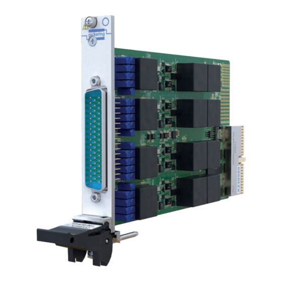
- Page 1 41/43-670 User Manual PXI/PXIe LVDT/RVDT/Resolver Simulator Module pickeringtest.com Issue 2.3 October 2022...
- Page 2 © COPYRIGHT (2022) PICKERING INTERFACES. ALL RIGHTS RESERVED. No part of this publication may be reproduced, transmitted, transcribed, translated or stored in any form, or by any means without the written permission of Pickering Interfaces. Technical details contained within this publication are subject to change without notice.
- Page 3 Pickering Interfaces strives to fulfil all relevant environmental laws and regulations and reduce wastes and releases to the environment. Pickering Interfaces aims to design and operate products in a way that protects the environment and the health and safety of its employees, customers and the public. Pickering Interfaces endeavours to develop and manufacture products that can be produced, distributed, used and recycled, or disposed of, in a safe and environmentally friendly manner.
- Page 4 PRODUCT SAFETY SAFETY SYMBOLS The following safety symbols may be used on the product and throughout the product documentation. MEANING / DESCRIPTION SYMBOL PROTECTIVE EARTH (GROUND) To identify any terminal which is intended for connection to an external conductor for protection against electric shock in case of a fault, or the terminal of a protective earth (ground) electrode.
-
Page 5: Table Of Contents
Hardware Installation ............3.2 Software Installation .............3.2 Testing Operation ..............3.3 Section 4 Programming Guide ..............4.1 Programming Options For Pickering PXI/PXIe Modules ...4.1 Using the Simulator Module ..........4.3 Programming the Input/Output Switches ......4.19 Programming Control - C# Functions .........4.21 Section 5 Connector Information ..............5.1 Section 6 Trouble Shooting .................6.1... - Page 6 THIS PAGE INTENTIONALLY BLANK PXI/PXIe LVDT/RVDT/Resolver Simulator Module 41/43-670 Page vi...
-
Page 7: Technical Specification
In applications where this is not acceptable, one of the outputs can be used to propagate the input 41-670 (PXI) and 43-670 (PXIe) are ideal for the simulation signal resulting in an in phase signal with the output which can of variable differential transformers (VDT), both linear (LVDT) then be used for demodulation. - Page 8 Module Version’s Part Number Suffix Output -xxxx01 -xxxx02 -xxxx03 -xxxx04 -xxxx05 Mechanical Characteristics Characteristics 41-670 - Single slot 3 U PXI (CompactPCI card). 0.45 V 0.9 V 1.8 V 3.5 V 43-670 - Single slot 3 U PXIe, compatible with PXIe Voltage hybrid slot.
- Page 9 Connection Solutions catalog. Product Customization Pickering modules are designed and manufactured on our own flexible manufacturing lines, giving complete product control and enabling simple customization to meet very specific requirements.
- Page 10 We provide a full range of supporting cable and connector solutions for all our switching products—20 connector families with 1200+ products. We offer everything from simple mating connectors to complex cables assemblies and terminal blocks. All assemblies are manufactured by Pickering and are guaranteed to mechanically and electrically mate to our modules. Connectors & Backshells...
- Page 11 Supporting Products & Software LVDT/RVDT/Resolver Simulator, 41/43-670 Programming Pickering provide kernel, IVI and VISA (NI & Keysight) drivers which are compatible with all Microsoft supported versions of Windows and popular older versions. For a list of all supporting operating systems, please see: pickeringtest.com/os The VISA driver is also compatible with Real-Time Operating Systems such as LabVIEW RT.
- Page 12 SECTION 1 - TECHNICAL SPECIFICATION pickering THIS PAGE INTENTIONALLY BLANK Page 1.6 PXI/PXIe LVDT/RVDT/Resolver Simulator Module 41/43-670...
-
Page 13: Technical Description
SECTION 2 - TECHNICAL DESCRIPTION pickering SECTION 2 - TECHNICAL DESCRIPTION FUNCTIONAL DESCRIPTION The 41/43-670 module can be supplied with between one and four banks which can be specified for the simulation of Linear Variable Differential Transformers (LVDT), Rotary Variable Differential Transformers (RVDT) or Resolvers. -
Page 14: Simulation Configurations
SECTION 2 - TECHNICAL DESCRIPTION pickering SIMULATION CONFIGURATIONS The 41/43-670 Simulator has up to 4 banks with consisting of four inputs and eight outputs, which may be set into different modes of operation: Mode 1 - 5/6-Wire (2 complementary outputs) •... - Page 15 Displacement Secondary LVDT 4-Wire Operation - Differential Output 41-670 Module 4-Wire Operation - Independent Outputs (Two Independent Channels - Common Excitation) Figure 2.4 - 4-Wire Operation of an LVDT In this mode the two outputs of the bank are controlled fully independently allowing simulation of two separate 4-wire LVDTs on each bank, the output will be the equivalent of combining both outputs of the 5/6 wire mode with the computation carried out internally.
- Page 16 SECTION 2 - TECHNICAL DESCRIPTION pickering THIS PAGE INTENTIONALLY BLANK Page 2.4 PXI/PXIe LVDT/RVDT/Resolver Simulator Module 41/43-670...
-
Page 17: Installation
Modular products require installation in a suitable PXI/PXIe/LXI chassis. The module is for indoor use only. PREOPERATION CHECKS (UNPACKING) 1. Check the module for transport damage and report any damage immediately to Pickering Interfaces. Do not attempt to install the product if any damage is evident. -
Page 18: Hardware Installation
For a system comprising more than one chassis, turn ON the last chassis in the system followed by the penultimate, etc, and finally turn ON the external controller or chassis containing the system controller. 9. For Pickering Interfaces modular LXI installation there is no requirement to use any particular power up sequence. -
Page 19: Testing Operation
Figure 3.2 - General Soft Front Panel Icon A selector panel will appear, listing all installed Pickering PCI, PXI or LXI switch cards and resistor cards. Click on the card you wish to control, and a graphical control panel is presented allowing operation of the card. - Page 20 SECTION 3 - INSTALLATION pickering THIS PAGE INTENTIONALLY BLANK Page 3.4 PXI/PXIe LVDT/RVDT/Resolver Simulator Module 41/43-670...
-
Page 21: Programming Guide
SECTION 4 - PROGRAMMING GUIDE PROGRAMMING OPTIONS FOR PICKERING INTERFACES PXI/PXIe MODULES For information on the installation and use of drivers and the programming of Pickering’s products in various software environments, please refer to the Software User Manual. This is available as a download from: https://www.pickeringtest.com/support/software-drivers-and-downloads... -
Page 22: Using The Simulator Module
SECTION 4 - PROGRAMMING GUIDE pickering USING THE SIMULATOR MODULE 41/43-670 LVDT Simulator Overview Output A Sampling LVDT Simulator Output B The LVDT Simulator continually samples the excitation input signal at 1.8MHz into a FIFO buffer, the output signal is automatically synchronised to align its phase to the input phase, this allows adjustment either way from the internal buffer in 555ns intervals to simulate phase offsets. - Page 23 SECTION 4 - PROGRAMMING GUIDE pickering Setting The Simulation Configuration The fully populated 41/43-670 Simulator has 4 banks and consists of four inputs and eight outputs, which may be set into several configurations to represent the desired hardware. This is illustrated by the Soft Front Panel’s Configuration screen.
- Page 24 SECTION 4 - PROGRAMMING GUIDE pickering LVDT Control Methods Figure 4.3 - Selecting a Control Method for Bank 1 The methods for controlling the Simulator module as follows: 1 - Percentage -100% to +100% • 2 - Percentage 0 to +100% •...
- Page 25 SECTION 4 - PROGRAMMING GUIDE pickering Input Gain NOTE: It is very important that the input gain is set to the optimum level. This is for the signal to be internally scaled correctly for maximum sampling resolution. Choose the correct version of LVDT simulator module to cover the desired input and output levels and excitation frequency, these specification limits are defined by hardware parameters.
- Page 26 SECTION 4 - PROGRAMMING GUIDE pickering Write Frequency & Set Input Level ‘Write Frequency’ can be used to fix the applied excitation frequency calculation, changes or even small variations in the excitation frequency will be ignored. Write 0 to measure the excitation frequency at the input.
- Page 27 SECTION 4 - PROGRAMMING GUIDE pickering Internally Generated Feature A feature has been implemented to generate an internal excitation, the driver calculates the waveform and uploads it to the internal circular buffer instead of from sampling the input. This allows a glitch free output without applying an input signal, each bank can be run independently at its own frequency and amplitude.
- Page 28 SECTION 4 - PROGRAMMING GUIDE pickering Set Sample Buffer Feature Input Attenuation Stage Average Frquency (Hz) The sample buffer size averages over the measured number of cycles of the input signal and uses these to calculate the input frequency, this calculation is used to apply phase correction to the output signals. A higher buffer size will give a more stable frequency measurement but if the input frequency is intentionally varied it will impose a delay.
- Page 29 SECTION 4 - PROGRAMMING GUIDE pickering Loss of Signal Threshold The LOS threshold can be used to set the minimum valid amplitude level of the applied input signal. In the event of loss of signal the frequency calculation is frozen. This allows the output to return immediately (within one cycle) in phase as soon as the same excitation frequency is reapplied, this saves the module retaking multiple samples of the input to calculate frequency and applying the correction.
- Page 30 SECTION 4 - PROGRAMMING GUIDE pickering Figure 4.9 - Set Loss of Signal Feature Figure 4.10 - Loss of Signal Detected PXI/PXIe LVDT/RVDT/Resolver Simulator Module 41/43-670 Page 4.10...
- Page 31 SECTION 4 - PROGRAMMING GUIDE pickering Channel Output Invert This function changes the phase the A or B outputs by 180° in relation to the excitation signal, outputs can be inverted separately or both outputs can be inverted if required. This means the polarity of the output connections is not critical as they can easily be inverted with this function.
- Page 32 SECTION 4 - PROGRAMMING GUIDE pickering Set Null Offset When dealing with very small LVDT positional changes, the extremes at -100% and +100% will not be zero, for this use the Null offset function to define the minimum voltage. This does not change the Vsum value it just applies a positive offset to the lower voltage.
- Page 33 SECTION 4 - PROGRAMMING GUIDE pickering VSum / VDiff Example Vsum / Vdiff is a different way of controlling an LVDT by setting the voltage characteristics. Vsum defines the maximum voltage of the LVDT outputs. Rather than position, Vdiff adjusts the difference between the two outputs A and B.
- Page 34 SECTION 4 - PROGRAMMING GUIDE pickering Phase Offset Alignment Interwinding and stray capacitance effects on the output phase angle can be replicated buy adjusting the output phase lag value. It can be adjusted from the zero ‘in phase’ reference position in 555ns increments, both outputs A and B can be adjusted independently.
- Page 35 SECTION 4 - PROGRAMMING GUIDE pickering Resolver Mode Selecting ‘Mode 3’ as the mode of operation on the configuration screen sets the simulator module into resolver mode. The bank controls for this mode are outlined below: Zone 3 Zone 2...
- Page 36 SECTION 4 - PROGRAMMING GUIDE pickering For controlling resolver rotation there are several functions available: “Start Rotation” - Will start the rotation based on the current set values shown in the “Speed in RPM” and • “Number of Turns” text boxes.
- Page 37 SECTION 4 - PROGRAMMING GUIDE pickering Attribute Codes ATTR_VDT_AUTO_INPUT_ATTEN = 0x450, /* Sets/Gets DWORD (0-100) for input gain (Default = 100) */ ATTR_VDT_VOLTAGE_SUM = 0x455, /* Sets/Gets DOUBLE in Volts for VSUM value */ ATTR_VDT_VOLTAGE_DIFF = 0x456, /* Sets/Gets DOUBLE in Volts for VDIFF value (the limit is +/- VSUM) */...
- Page 38 SECTION 4 - PROGRAMMING GUIDE pickering ATTR_VDT_LOS_THRESHOLD = 0x465, /* Sets/Gets DWORD (0 to 32768) for LOS Threshold (Default = 32768) */ ATTR_VDT_SMPL_BUFFER_SIZE = 0x466, /* Sets/Gets DWORD (1 to 500) for Sample buffer size (Default = 500) */ ATTR_VDT_NULL_OFFSET...
- Page 39 SECTION 4 - PROGRAMMING GUIDE pickering Attributes Specific to Resolver ATTR_RESOLVER_START_STOP_ROTATE = 0x470, /* Sets/Gets BOOL TRUE for Start, FALSE of Stop */ ATTR_RESOLVER_NUM_OF_TURNS = 0x471, /* Sets/ Gets WORD Number of turns (1-65535) */ ATTR_RESOLVER_ROTATE_SPEED = 0x472, /* Sets/Gets DOUBLE rotating speed (RPM speed upto 655.35 RPM) */...
-
Page 40: Programming The Input/Output Switches
SECTION 4 - PROGRAMMING GUIDE pickering PROGRAMMING THE INPUT/OUTPUT SWITCHES Each LVDT simulation bank has switches on the inputs and output to enable short and open circuit conditions for fault simulation. Also switching is included for interconnecting inputs so that a common excitation signal can be shared between channels. - Page 41 SECTION 4 - PROGRAMMING GUIDE pickering Sub-unit 5 Channel 1 bit 5 OUTA_S_1 Sub-unit 5 bit 7 bit 1 bit 3 bit 6 IN_S_1 OUTA_G_1 Signal bit 4 bit 11 Processing bit 8 IN_G_1 OUTB_S_1 bit 2 bit 10 bit 9...
-
Page 42: Programming Control - C# Functions
SECTION 4 - PROGRAMMING GUIDE pickering PROGRAMMING CONTROL - C# FUNCTIONS Set Mode Function The Set Mode function allows you to choose between 5/6-Wire, 4-Wire or Resolver functionality (if it is available on the card). BYTE setMode = 1; // Set Mode 5_6_Wire DWORD sub = 1;... - Page 43 SECTION 4 - PROGRAMMING GUIDE pickering Python Example Code switchSub = 5 #Switch Sub-unit bankOffset = 11 bank = 2 # LVDT Bank (Sub-Unit) number #Input Switches error = card.OpBit(switchSub, ((bank - 1) * bankOffset) + 1, True) error = card.OpBit(switchSub, ((bank - 1) * bankOffset) + 2, True) error = card.OpBit(switchSub, ((bank - 1) * bankOffset) + 3, True) error: # This function will take an error code and return a string description of the error err, errorString = card.ErrorMessage(error)
- Page 44 SECTION 4 - PROGRAMMING GUIDE pickering #Set Speed speed = 50.00 # Set speed between 1.00 - 655.35 RPM error = card.ResolverSetRotateSpeed(bank, speed) error: # This function will take an error code and return a string description of the error err, errorString = card.ErrorMessage(error)
- Page 45 SECTION 5 - CONNECTOR INFORMATION pickering SECTION 5 - CONNECTOR INFORMATION OUTB_S_1 IN_S_1 OUTA_S_1 OUTB_G_1 IN_G_1 OUTA_G_1 OUTB_S_2 IN_S_2 OUTA_S_2 OUTB_G_2 IN_G_2 OUTA_G_2 OUTB_S_3 IN_S_3 OUTA_S_3 OUTB_G_3 IN_G_3 OUTA_G_3 OUTB_S_4 IN_S_4 OUTA_S_4 OUTB_G_4 IN_G_4 OUTA_G_4 FP_GND Figure 5.1 - Pinouts: PXI 4-Bank LVDT/RVDT/Resolver Simulator Module 41/43-670 (50-pin Male D-Type Connector Viewed From Front of Module) Page 5.1...
- Page 46 SECTION 5 - CONNECTOR INFORMATION pickering THIS PAGE INTENTIONALLY BLANK Page 5.2 PXI/PXIe LVDT/RVDT/Resolver Simulator Module 41/43-670...
-
Page 47: Trouble Shooting
PCI configuration, highlighting any potential configuration problems. Specific details of all installed Pickering switch cards are included. All the installed Pickering switch cards should be listed in the “Pilpxi information” section - if one or more cards is missing it may be possible to determine the reason by referring to the PCI configuration dump contained in the report, but interpretation of this information is far from straightforward, and the best course is to contact Pickering support: support@pickeringtest.com, if possible... - Page 48 SECTION 6 - TROUBLE SHOOTING pickering THIS PAGE INTENTIONALLY BLANK Page 6.2 PXI/PXIe LVDT/RVDT/Resolver Simulator Module 41/43-670...
-
Page 49: Maintenance Information
For PXI modules which are supported in one of Pickering Interfaces’ Modular LXI Chassis (such as the 60-102B and 60-103B) no module software update is required. If the module was introduced after the LXI chassis was manufactured the module may not be recognized, in this case the chassis firmware may need upgrading. -
Page 50: Verification Procedure
SECTION 7 - MAINTENANCE INFORMATION pickering VERIFICATION PROCEDURE 6½ Digit DMM Signal Generator - 300Hz to 20kHz 41/43-670 Calibration/ Verification Cable V, + V, - OUTA_S_1-4 IN_S_1-4 OUTA_G_1-4 IN_G_1-4 6½ Digit DMM V, + V, - OUTB_S_1-4 OUTB_G_1-4 Figure 7.1 - 41/43-670 Gain and Linearity Verification Connections... - Page 51 SECTION 7 - MAINTENANCE INFORMATION pickering Each channel can be independently verified using the following steps. Results from this verification can be recorded in the results tables on pages 7.6 to 7.13. Outputs A and B of all channels can be connected in parallel, as shown in figure X.X. This is achieved by •...
- Page 52 SECTION 7 - MAINTENANCE INFORMATION pickering Resolver Gain Verification Procedure Setup • 1. Close all the required input and output relays 2. Adjust input attenuator 3. Set channel mode to resolver 4. Set the maximum output level (VSUM) to its minimum setting according to Table 7.1 to 7.5 (depending...
- Page 53 SECTION 7 - MAINTENANCE INFORMATION pickering Table 7.1 - Gain Verification Test Results For -xxxx01 Serial Number: Channel Number: Date of Test: Operator’s Name: Test Equipment Used: Result (delete VSUM Measurement A Measurement B Minimum [VRMS] Maximum [VRMS] as appropriate) 0.450...
- Page 54 SECTION 7 - MAINTENANCE INFORMATION pickering Table 7.3 - Gain Verification Test Results For -xxxx03 Serial Number: Channel Number: Date of Test: Operator’s Name: Test Equipment Used: Result (delete VSUM Measurement A Measurement B Minimum [VRMS] Maximum [VRMS] as appropriate) 1.800...
- Page 55 SECTION 7 - MAINTENANCE INFORMATION pickering Table 7.5 - Gain Verification Test Results For -xxxx05 Serial Number: Channel Number: Date of Test: Operator’s Name: Test Equipment Used: Result (delete VSUM Measurement A Measurement B Minimum [VRMS] Maximum [VRMS] as appropriate) 7.000...
- Page 56 SECTION 7 - MAINTENANCE INFORMATION pickering Table 7.7 - Linearity Verification Test Results For Resolver Simulator -xxxx01 Serial Number: Channel Number: Date of Test: Operator’s Name: Test Equip- ment Used: Measured Measured Result (delete Position Minimum Maximum Minimum Maximum as appropriate) -180.00...
- Page 57 SECTION 7 - MAINTENANCE INFORMATION pickering Table 7.8 - Linearity Verification Test Results For Resolver Simulator -xxxx02 Serial Number: Channel Number: Date of Test: Operator’s Name: Test Equip- ment Used: Measured Measured Result (delete Position Minimum Maximum Minimum Maximum as appropriate) -180.00...
- Page 58 SECTION 7 - MAINTENANCE INFORMATION pickering Table 7.9 - Linearity Verification Test Results For Resolver Simulator -xxxx03 Serial Number: Channel Number: Date of Test: Operator’s Name: Test Equip- ment Used: Measured Measured Result (delete Position Minimum Maximum Minimum Maximum as appropriate) -180.00...
- Page 59 SECTION 7 - MAINTENANCE INFORMATION pickering Table 7.10 - Linearity Verification Test Results For Resolver Simulator -xxxx04 Serial Number: Channel Number: Date of Test: Operator’s Name: Test Equip- ment Used: Measured Measured Result (delete Position Minimum Maximum Minimum Maximum as appropriate) -180.00...
- Page 60 SECTION 7 - MAINTENANCE INFORMATION pickering Table 7.11 - Linearity Verification Test Results For Resolver Simulator -xxxx05 Serial Number: Channel Number: Date of Test: Operator’s Name: Test Equip- ment Used: Measured Measured Result (delete Position Minimum Maximum Minimum Maximum as appropriate) -180.00...
-
Page 61: Relay Look-Up Table
SECTION 7 - MAINTENANCE INFORMATION pickering RELAY LOOK-UP TABLE The following table shows the relationship between the function of the input and output switching networks and the corresponding relay number on the circuit board. This can be used in conjunction with the PCB layout diagram in Figure 7.2 for locating faulty relays. - Page 62 SECTION 7 - MAINTENANCE INFORMATION pickering Bank 4 Bank 3 Bank 2 Bank 1 Figure 7.2 - 41/43-670 LVDT/RVDT/Resolver Simulator Module - Relay Locations Page 7.14 PXI/PXIe LVDT/RVDT/Resolver Simulator Module 41/43-670...
Need help?
Do you have a question about the 41-670 and is the answer not in the manual?
Questions and answers