Table of Contents
Advertisement
Quick Links
Please refer to the original service manual for:
DVD Mechanism Unit (BRS12D), Order No. PSG1408009AE
Speaker system SB-AKX18PN-K, Order No. PSG1401008CE
TABLE OF CONTENTS
1 Safety Precautions----------------------------------------------- 3
1.1. General Guidelines---------------------------------------- 3
1.2. Before Repair and Adjustment ------------------------- 4
1.3. Protection Circuitry ---------------------------------------- 4
1.4. Caution For AC Cord (For GS only) ------------------ 5
1.5. Power Supply using SMPS ----------------------------- 6
1.6. Safety Parts Information --------------------------------- 6
2 Warning -------------------------------------------------------------- 7
to Electrostatically Sensitive (ES) Devices---------- 7
2.2. Precaution of Laser Diode------------------------------- 7
(PbF)---------------------------------------------------------- 8
2.4. Handling Precautions for Traverse Unit-------------- 8
prevention --------------------------------------------------- 9
3 Service Navigation ----------------------------------------------10
PAGE
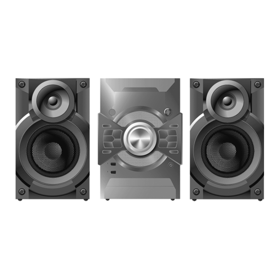
DVD Stereo System
SA-VKX25EE
Model No.
SA-VKX25GA
SA-VKX25GS
Product Color: (K)...Black Type
3.1. Service Information -------------------------------------- 10
4 Specifications ---------------------------------------------------- 11
5 Location of Controls and Components------------------ 12
5.1. Remote Control Key Button Operation ------------- 12
5.2. Main Unit Key Button Operation---------------------- 13
6 Service Mode ----------------------------------------------------- 14
6.1. Service Mode Table ------------------------------------- 14
6.2. Sales Demonstration Lock Function ---------------- 14
6.3. Doctor Mode Table--------------------------------------- 15
6.4. Error Code Table ----------------------------------------- 18
6.5. Self-Diagnostic Mode ----------------------------------- 19
6.6. Self Diagnostic Function-Error Code---------------- 24
6.7. Firmware Version-Up Information-------------------- 25
7 Troubleshooting Guide --------------------------------------- 28
7.1. No Power or No Display-------------------------------- 28
7.2. Bluetooth® Pairing Failure----------------------------- 28
7.3. No Key Function------------------------------------------ 28
© Panasonic Corporation 2014. All rights reserved.
Unauthorized copying and distribution is a violation
of law.
PSG1409002CE
PAGE
Advertisement
Table of Contents

Related Manuals for Panasonic SA-VKX25EE


Summary of Contents for Panasonic SA-VKX25EE
-
Page 1: Table Of Contents
7.1. No Power or No Display-------------------------------- 28 prevention --------------------------------------------------- 9 7.2. Bluetooth® Pairing Failure----------------------------- 28 3 Service Navigation ----------------------------------------------10 7.3. No Key Function------------------------------------------ 28 © Panasonic Corporation 2014. All rights reserved. Unauthorized copying and distribution is a violation of law. - Page 2 7.4. No Remote Control Function -------------------------- 28 15.4. Mechanical Replacement Part List ------------------ 91 7.5. USB Device Cannot Detect---------------------------- 29 15.5. Electrical Replacement Parts List ------------------- 93 7.6. No Output Sound----------------------------------------- 30 7.7. Check Point------------------------------------------------ 31 8 Disassembly and Assembly Instructions --------------- 34 8.1.
-
Page 3: Safety Precautions
1 Safety Precautions 1.1. General Guidelines 1. IMPORTANT SAFETY NOTICE There are special components used in this equipment which are important for safety. These parts are marked by in the Schematic Diagrams, Circuit Board Layout, Exploded Views and Replacement Parts List. It is essential that these critical parts should be replaced with manufacturer’s specified parts to prevent X-RADIATION, shock, fire, or other hazards. -
Page 4: Before Repair And Adjustment
1.2. Before Repair and Adjustment Disconnect Power Supply AC to discharge AC capacitor as indicate below diagram (in SMPS Module) through a 10 W, 10 W resis- tor to ground. Figure 1-2 Caution: DO NOT SHORT-CIRCUIT DIRECTLY (with a screwdriver blade, for instance), as this may destroy solid state devices. After repairs are completed, restore power gradually using a variac to avoid overcurrent. -
Page 5: Caution For Ac Cord (For Gs Only)
1.4. Caution For AC Cord (For GS only) Figure 1-3... -
Page 6: Power Supply Using Smps
1.5. Power Supply using SMPS This model uses Switching Mode Power Supply (SMPS) to provide the power supply to the unit. Here is the supplied part no. for the SMPS Module 1) N0AC2GK00001 Figure 1-4 1.6. Safety Parts Information Safety Parts List: There are special components used in this equipment which are important for safety. -
Page 7: Warning
2 Warning 2.1. Prevention of Electrostatic Discharge (ESD) to Electrostatically Sensi- tive (ES) Devices Some semiconductor (solid state) devices can be damaged easily by static electricity. Such components commonly are called Elec- trostatically Sensitive (ES) Devices. The following techniques should be used to help reduce the incidence of component damage caused by electrostatic discharge (ESD). -
Page 8: General Description About Lead Free Solder (Pbf)
Figure 2-1 2.3. General description about Lead Free Solder (PbF) The lead free solder has been used in the mounting process of all electrical components on the printed circuit boards used for this equipment in considering the globally environmental conservation. The normal solder is the alloy of tin (Sn) and lead (Pb). -
Page 9: Grounding For Electrostatic Breakdown Prevention
3. The flexible cable may be cut off if an excessive force is applied to it. Use caution when handling the flexible cable. 4. The antistatic FFC is connected to the new optical pickup unit. After replacing the optical pickup unit and connecting the flexi- ble cable, cut off the antistatic FFC. -
Page 10: Service Navigation
3 Service Navigation 3.1. Service Information This service manual contains technical information which will allow service personnel’s to understand and service this model. Please place orders using the parts list and not the drawing reference numbers. If the circuit is changed or modified, this information will be followed by supplement service manual to be filed with original service manual. -
Page 11: Specifications
USB port power 500 mA (max) Bit rate Up to 4 Mbps (Xvid) System: SC-VKX25EE-K USB Recording Main Unit: SA-VKX25EE-K Bit rate 128 kbps Front Speakers: SB-AKX18PN-K USB recording speed Recording file format MP3 (*.mp3) System: SC-VKX25GA-K Main Unit: SA-VKX25GA-K ®... -
Page 12: Location Of Controls And Components
5 Location of Controls and Components 5.1. Remote Control Key Button Operation... -
Page 13: Main Unit Key Button Operation
5.2. Main Unit Key Button Operation... -
Page 14: Service Mode
6 Service Mode 6.1. Service Mode Table 6.2. Sales Demonstration Lock Function... -
Page 15: Doctor Mode Table 1
6.3. Doctor Mode Table 6.3.1. Doctor Mode Table 1 Item Key Operation FL Display Mode Name Description Front Key Doctor Mode To enter into Doctor Mode In CD Mode: 1. Press [ ] button on main unit follow by [4] and [7] on remote control. - Page 16 6.3.2. Doctor Mode Table 2 Item Key Operation FL Display Mode Name Description Front Key Volume Setting To check the volume setting of the In Doctor Mode: Check main unit. 1. Press below button on the remote control. Press [7]: VOL50 Volume Press [8]: VOL35 Press [9]: VOL0...
- Page 17 6.3.3. Doctor Mode Table 3 Key Operation Item FL Display Mode Name Description Front Key Bluetooth Bluetooth module will need some 1. Go to Bluetooth selector and Version Check time to power up and read the then enter Doctor Mode. ( 2 sec) version display.
-
Page 18: Error Code Table
6.4. Error Code Table Self-Diagnostic Function provides information on any problems occurring for the unit and its respective components by displaying the error codes. These error code such as U**, H** and F** are stored in memory and held unless it is cleared. The error code is automatically display after entering into self-diagnostic mode. -
Page 19: Self-Diagnostic Mode
6.5. Self-Diagnostic Mode 6.5.1. Self-Diagnostic Mode Table 1 (For DVD Module) - Page 20 6.5.2. Self-Diagnostic Mode Table 2 (For DVD Module)
- Page 21 6.5.3. Self-Diagnostic Mode Table 3 (For DVD Module)
- Page 22 6.5.4. Self-Diagnostic Mode Table 4 (For DVD Module) Item FL Display Key Operation Mode Name Description Timer 1 check Timer 1 check In DVD/CD (no disc) Mode: (Display 1) Laser operation timer is measured Press [STOP] separately for DVD laser and CD laser. button on the main unit, and [ ] button on the...
- Page 23 6.5.5. Video Design Information Product Region TV Broadcasting Model Country Region Signal System Region Display Series Code System OSD Menu Language (Default) (Default) Default P, PC, USA, Canada, English (NA), Spanish (NA), NTSC NTSC (*A) English US Militry Canadian French Japan NTSC NTSC (*A)
-
Page 24: Self Diagnostic Function-Error Code
6.6. Self Diagnostic Function-Error Code 6.6.1. Mechanism Error Code Table 6.6.2. DVD Module Error Code Table... -
Page 25: Firmware Version-Up Information
6.7. Firmware Version-Up Information 6.7.1. Process Flow (1/3) Item FL/ GUI Display Remarks Process Description Collect ROM There are 2 files: User can put both files Files A) Syscon ROM file type: into the same root (Copy files into Display 1: directory. - Page 26 6.7.2. Process Flow (2/3) Item FL/ GUI Display Remarks Process Description GUI Display 1.3.2: GUI Display 1.3.2: UPDATING WRITING TO FLASHROM FL Display 2: Update stop Check Correct ROM files doesn't fit to the (Wrong ROM Type) ROM file type product type.
- Page 27 6.7.3. Process Flow (3/3) Item FL/ GUI Display Remarks Process Description 1. Update Failed Update software Update stop. FL Display 4: (Opecon) The theater set can't work, If Opecon software update fail: and can't be recovered by FL Display 3: "FAIL" . CD update again.
-
Page 28: Troubleshooting Guide
7 Troubleshooting Guide 7.1. No Power or No Display Caution: Check Primary E-Cap Press Power Button Check Secondary Cap. (C9 & C22) 1. AC Cord Plug-out No Display on (C1 & C2) of Unit or Remote Control Measured 38.5V 2. Check Fuse(F1) = 0 ohm FL Panel Measured 150V or more to Turn ON the Unit... -
Page 29: Usb Device Cannot Detect
7.5. USB Device Cannot Detect Press Power Button Press [SELECTOR and Press Play No Problem Plug-in USB Device choose USB mode] on the Set of Unit or Remote Control FL Display or Use Remote Control Found FL Display "USB" to Turn ON the Unit "Music Name or Title"... -
Page 30: No Output Sound
7.6. No Output Sound DVD/CD Play Press Power Button Press Play No Problem of Unit or Remote Control Output Sound DVD/CD Mode FL Display "Track & Count" Found to Turn ON the Unit Check CD Mechanism / Check Traverse Unit Main PCB Checking Points: 1) IC4001 (DSP IC) pin 4 (I/P) &... -
Page 31: Check Point
7.7. Check Point Power PCB Pri. Cap (C1) Pri. Cap Sec. Cap. (C2) (C20) Fuse (F1) C1 & C2 (150V) (0 ohm) (32.5V) - Page 32 Main PCB IC1000_Pin#2 (3.3V) IC2103_Pin#10 (15V) CN2506_Pin#20 (15V) IC2107_Pin#2 (1.5V) IC2108_Pin#2 (3.3V) CN2511 Bluetooth Pin#6 & Pin#7 IC7701_Pin 9 (5V) (5V)
- Page 33 BACK-END PCB FP8101 Pin#5, Pin#7, Pin#9, Pin#11 (5V)
-
Page 34: Disassembly And Assembly Instructions
8 Disassembly and Assembly Instructions • This section describes the disassembly and/or assembly procedures for all major printed circuit boards & main compo- nents for the unit. (You may refer to the section of “Main components and P.C.B. Locations” as described in this service manual) •... -
Page 35: Main Components And P.c.b. Locations
8.3. Main Components and P.C.B. Locations... -
Page 36: Disassembly Of Top Cabinet
8.4. Disassembly of Top Cabinet 8.5. Disassembly of Front Panel Unit Step 1 Remove 4 screws. Step 2 Remove 5 screws. • Refer to “Disassembly of Top Cabinet”. Step 3 Release both sides of Top Cabinet outwards as arrow shown. Step 1 Detach 8P Wire at the connector (CN2511) on Main P.C.B.. -
Page 37: Disassembly Of Panel P.c.b. And Music Port P.c.b
8.6. Disassembly of Panel P.C.B. Step 5 Release tabs at bottom of unit. Step 6 Detach to remove Front Panel Unit and Music Port P.C.B. • Refer to “Disassembly of Top Cabinet”. • Refer to “Disassembly of Front Panel Unit”. Step 1 Remove Volume Knob. -
Page 38: Disassembly Of Usb P.c.b
8.8. Disassembly of Rear Panel. Step 5 Remove Panel P.C.B. and Music Port P.C.B.. • Refer to “Disassembly of Top Cabinet”. Step 1 Remove 9 screws. 8.7. Disassembly of USB P.C.B. • Refer to “Disassembly of Top Cabinet”. Step 2 Lift up to detach Chassis Unit. •... -
Page 39: Disassembly Of Main P.c.b
8.9. Disassembly of Main P.C.B. 8.10. Disassembly of SMPS Module • Refer to “Disassembly of Top Cabinet”. • Refer to “Disassembly of Top Cabinet”. • Refer to “Disassembly of Rear Panel”. • Refer to “Disassembly of Rear Panel”. Step 1 Detach 10P Cable at the connector (CON2) on SMPS Step 1 Detach 10P Cable at the connector (CON2) on SMPS Module. -
Page 40: Disassembly Of Dvd Mechanism Unit
8.11. Disassembly of DVD Mecha- Step 5 Release catches. Step 6 Lift up to remove Inner Chassis Unit. nism Unit • Refer to “Disassembly of Top Cabinet”. • Refer to “Disassembly of Front Panel Unit”. Step 1 Remove 7 screws. Step 7 Remove 2 screws. -
Page 41: Disassembly Of Backend P.c.b. Ass'y
Step 8 Detach 5P FFC at the connector (FP8252) on Backend P.C.B. Ass’y. Step 9 Detach 6P FFC at the connector (FP8251) on Backend P.C.B. Ass’y. Step 10 Detach 24P FFC at the connector (FP8531) on Back- end P.C.B. Ass’y. Step 11 Remove DVD Mechanism Unit. -
Page 42: Service Position
9 Service Position Note: For description of the disassembly procedures, see the Section 8. 9.1. Checking of Panel P.C.B. and 9.2. Checking and Repairing of Music Port P.C.B. Main P.C.B. and SMPS Module Step 1 Remove Top Cabinet. Step 1 Remove Top Cabinet. Step 2 Remove Front Panel Unit. -
Page 43: Checking And Repairing Of Backend P.c.b. Ass'y
9.3. Checking and Repairing of Step 10 Place Backend P.C.B. Ass'y on the insulated material. Step 11 Attach 5P FFC at the connector (FP8252) on Backend Backend P.C.B. Ass'y P.C.B. Ass'y. Step 12 Attach 6P FFC at the connector (FP8251) on Backend Step 1 Remove Top Cabinet. -
Page 45: Block Diagram
LD CCW LD CCW LD CCW INNER SW FP8101 FP5001 INNER SW INNER SW FP8252 FP8101 FP5001 CLOSE SW CLOSE SW CLOSE SW CLOSE SW FP8252 FP8101 FP5001 OPEN SW OPEN SW OPEN SW OPEN SW SA-VKX25EE/GA/GS BACKEND (1/2) BLOCK DIAGRAM... - Page 46 USB2 D+ USB2 D+ 144 LOUT DAC2OUT 13 CBIN CN2505 FP9001 USB2 D- USB2 D- USB2 D- 146 ROUT DAC3OUT 15 CRIN FROM/TO SYSTEM CONTROL 5 MUTE1 Q2801 VMUTE FP5001 FP8101 VMUTE MUTING VMUTE CONTROL SA-VKX25EE/GA/GS BACKEND (2/2) BLOCK DIAGRAM...
-
Page 47: System Control
VMUTE VMUTE ECK 34 6 SCL DVD CMD DV5 CMD TO SYSTEM CONTROL BLOCK (2/3) TO POWER SUPPLY DVD PCONT DVD PCON IC2300 RFKWMVKX25GM MICROPROCESSOR NOTE: “ * ” REF IS FOR INDICATION ONLY SA-VKX25EE/GA/GS SYSTEM CONTROL (1/3) BLOCK DIAGRAM... - Page 48 ALBUM/TRACK EEPROM SCL S6212 S6217 LOCAL PRESET EQ D6207 S6213 S6218 MANUAL EQ D6203 PLAY/PAUSE D6208 S6219 RADIO/AUX D6209 S6214 D.BASS S6220 D6204 DVD/CD D6210 SG10 S6215 D6205 REC/PAUSE TO SYSTEM CONTROL BLOCK (1/3) SA-VKX25EE/GA/GS SYSTEM CONTROL (2/3) BLOCK DIAGRAM...
- Page 49 TUN INT NRST NRST TUN SDO TUN SDO SYNC SYNC SOC MCLK SOC MCLK DC DET PWR PDET DC DET AMP DCDET DC DET PWR NOTE: “ * ” REF IS FOR INDICATION ONLY SA-VKX25EE/GA/GS SYSTEM CONTROL (3/3) BLOCK DIAGRAM...
-
Page 50: Audio
TUN RST FROM/TO SYSTEM CONTROL TUN WCK DFS 14 DCLK 17 TUN BCK SCLK SDIO IC52 I2C SDA VUEALLPT087 FROM/TO AM/FM RADIO SYSTEM CONTROL I2C SCL RECEIVER NOTE: “ * ” REF IS FOR INDICATION ONLY SA-VKX25EE/GA/GS AUDIO BLOCK DIAGRAM... -
Page 51: Power Supply
VO 3 +1.8V +3.3V 4 VIN ZJ1002 STBY PCONT STBY PCONT ZJ1002 PROTECT PROTECT ZJ1002 SMPS ID FROM/TO SMPS ID SYSTEM CONTROL ZJ1002 TO POWER SUPPLY TEMP DET TEMP DET BLOCK (2/2) ZJ1002 SYNC SYNC SA-VKX25EE/GA/GS POWER SUPPLY (1/2) BLOCK DIAGRAM... - Page 52 +1.2V 1 VCC 1.2V 7 PW DVD +3R3V 3 VCC D+3.3V 6 +3.3V NRESET NRESET RST O 2 TO BACKEND TO POWER SUPPLY BLOCK (1/2) NOTE: “ * ” REF IS FOR INDICATION ONLY SA-VKX25EE/GA/GS POWER SUPPLY (2/2) BLOCK DIAGRAM...
-
Page 53: Wiring Connection Diagram
11 Wiring Connection Diagram TO SMPS MODULE ZJ1002* USB P.C.B. ZJ6401* MAIN P.C.B. ASS'Y CN2511 PANEL P.C.B. CN2506 CN2505 FP5001 CN6001 ZJ6000* BACKEND P.C.B. ASS'Y FP9001 CN6300 FP8252 FP8101 TO LOADING P.C.B. FP8531 (DVD MECHANISM UNIT) FP8251 6P MUSIC PORT P.C.B. TO TRAVERSE P.C.B. -
Page 55: Schematic Diagram
12 Schematic Diagram 12.1. Schematic Diagram Notes • This schematic diagram may be modified at any time with the development of new technology. Notes: S6200: Power ( ) switch. S6201: Open/Close ( ) switch. S6202: Stop ( )/Tune Mode switch. S6211: DJ Jukebox switch. -
Page 57: Backend (Dv5U) Circuit (1/4)
G1C100M00049 R8409 DV: BACKEND (DV5U): SCHEMATIC DIAGRAM - 1 ~ 4 RX8001 D1H41032A014 MD: BACKEND (MOTOR DRIVER): SCHEMATIC DIAGRAM - 5 VI: BACKEND (VIDEO): SCHEMATIC DIAGRAM - 6 C8505 RX8031 D1H44722A014 TO BACKEND (DV5U) SA-VKX25EE/GA/GS CIRCUIT (3/4) BACKEND (DV5U) CIRCUIT... -
Page 58: Backend (Dv5U) Circuit (2/4)
Q8565 DVD LASER DRIVE B1ABDF000026 R8552 SWITCH DV: BACKEND (DV5U): SCHEMATIC DIAGRAM - 1 ~ 4 TO BACKEND (DV5U) MD: BACKEND (MOTOR DRIVER): SCHEMATIC DIAGRAM - 5 CIRCUIT (4/4) VI: BACKEND (VIDEO): SCHEMATIC DIAGRAM - 6 SA-VKX25EE/GA/GS BACKEND (DV5U) CIRCUIT... -
Page 59: Backend (Dv5U) Circuit (3/4)
R8001 IC8651 MDQ_15 MDQ_0 RFKFVKX95GB DQ15 C8051 FLASH MEMORY IC8051 C3ABPY000090 SDRAM DV: BACKEND (DV5U): SCHEMATIC DIAGRAM - 1 ~ 4 MD: BACKEND (MOTOR DRIVER): SCHEMATIC DIAGRAM - 5 VI: BACKEND (VIDEO): SCHEMATIC DIAGRAM - 6 SA-VKX25EE/GA/GS BACKEND (DV5U) CIRCUIT... -
Page 60: Backend (Dv5U) Circuit (4/4)
R8230 2.2K R8231 2.4K TRV_DRV C8231 C8232 0.082 DRV1 R8232 5.6K SP_DRV DV: BACKEND (DV5U): SCHEMATIC DIAGRAM - 1 ~ 4 MD: BACKEND (MOTOR DRIVER): SCHEMATIC DIAGRAM - 5 VI: BACKEND (VIDEO): SCHEMATIC DIAGRAM - 6 SA-VKX25EE/GA/GS BACKEND (DV5U) CIRCUIT... -
Page 61: Backend (Motor Driver) Circuit
J0JHC0000117 PW_M_+5V C8557 C8251 6.3V100 R8270 K8252 D_GND IC8252 C0ABGA000090 OP-AMP DV: BACKEND (DV5U): SCHEMATIC DIAGRAM - 1 ~ 4 MD: BACKEND (MOTOR DRIVER): SCHEMATIC DIAGRAM - 5 VI: BACKEND (VIDEO): SCHEMATIC DIAGRAM - 6 SA-VKX25EE/GA/GS BACKEND (MOTOR DRIVER) CIRCUIT... -
Page 62: Backend (Video) Circuit
CBOUT R3807 CBIN CBSAG R3805 MUTE2 GND2 R3806 CRIN CROUT VCC2 CRSAG DV: BACKEND (DV5U): SCHEMATIC DIAGRAM - 1 ~ 4 MD: BACKEND (MOTOR DRIVER): SCHEMATIC DIAGRAM - 5 VI: BACKEND (VIDEO): SCHEMATIC DIAGRAM - 6 SA-VKX25EE/GA/GS BACKEND (VIDEO) CIRCUIT... -
Page 63: Main (Up) Circuit
DS: MAIN (DSP): SCHEMATIC DIAGRAM - 11 DA: MAIN (DAMP): SCHEMATIC DIAGRAM - 12 VR: MAIN (VOLTAGE REGULATOR): SCHEMATIC DIAGRAM - 13 SA-VKX25EE/GA/GS MAIN (UP) CIRCUIT CN: MAIN (CONNECTOR): SCHEMATIC DIAGRAM - 14 BT: MAIN (BLUETOOTH): SCHEMATIC DIAGRAM - 15... -
Page 64: Main (Soc) Circuit
DS: MAIN (DSP): SCHEMATIC DIAGRAM - 11 AGND AGND DA: MAIN (DAMP): SCHEMATIC DIAGRAM - 12 VR: MAIN (VOLTAGE REGULATOR): SCHEMATIC DIAGRAM - 13 CN: MAIN (CONNECTOR): SCHEMATIC DIAGRAM - 14 R1181...VKX25 BT: MAIN (BLUETOOTH): SCHEMATIC DIAGRAM - 15 R1183...GA SA-VKX25EE/GA/GS MAIN (SOC) CIRCUIT R1184...GS R1185...EE... -
Page 65: Main (Usb) Circuit
DS: MAIN (DSP): SCHEMATIC DIAGRAM - 11 DA: MAIN (DAMP): SCHEMATIC DIAGRAM - 12 VR: MAIN (VOLTAGE REGULATOR): SCHEMATIC DIAGRAM - 13 CN: MAIN (CONNECTOR): SCHEMATIC DIAGRAM - 14 BT: MAIN (BLUETOOTH): SCHEMATIC DIAGRAM - 15 SA-VKX25EE/GA/GS MAIN (USB) CIRCUIT... -
Page 66: Main (Tuner Aux) Circuit
DS: MAIN (DSP): SCHEMATIC DIAGRAM - 11 DA: MAIN (DAMP): SCHEMATIC DIAGRAM - 12 VR: MAIN (VOLTAGE REGULATOR): SCHEMATIC DIAGRAM - 13 CN: MAIN (CONNECTOR): SCHEMATIC DIAGRAM - 14 SA-VKX25EE/GA/GS MAIN (TUNER AUX) CIRCUIT BT: MAIN (BLUETOOTH): SCHEMATIC DIAGRAM - 15... -
Page 67: Main (Dsp) Circuit
DS: MAIN (DSP): SCHEMATIC DIAGRAM - 11 DA: MAIN (DAMP): SCHEMATIC DIAGRAM - 12 VR: MAIN (VOLTAGE REGULATOR): SCHEMATIC DIAGRAM - 13 CN: MAIN (CONNECTOR): SCHEMATIC DIAGRAM - 14 SA-VKX25EE/GA/GS MAIN (DSP) CIRCUIT BT: MAIN (BLUETOOTH): SCHEMATIC DIAGRAM - 15... -
Page 68: Main (Damp) Circuit
DS: MAIN (DSP): SCHEMATIC DIAGRAM - 11 DA: MAIN (DAMP): SCHEMATIC DIAGRAM - 12 VR: MAIN (VOLTAGE REGULATOR): SCHEMATIC DIAGRAM - 13 CN: MAIN (CONNECTOR): SCHEMATIC DIAGRAM - 14 SA-VKX25EE/GA/GS MAIN (DAMP) CIRCUIT BT: MAIN (BLUETOOTH): SCHEMATIC DIAGRAM - 15... -
Page 69: Main (Voltage Regulator) Circuit
DA: MAIN (DAMP): SCHEMATIC DIAGRAM - 12 IC2101 PW_SMPS_5V VR: MAIN (VOLTAGE REGULATOR): SCHEMATIC DIAGRAM - 13 C0DBAYY01594 PWR_GND DAMP_GND +5V DC-DC CONVERTER CN: MAIN (CONNECTOR): SCHEMATIC DIAGRAM - 14 PWR_GND BT: MAIN (BLUETOOTH): SCHEMATIC DIAGRAM - 15 PW_+32V PW_+32V SA-VKX25EE/GA/GS MAIN (VOLTAGE REGULATOR) CIRCUIT... -
Page 70: Main (Connector) Circuit
DS: MAIN (DSP): SCHEMATIC DIAGRAM - 11 DA: MAIN (DAMP): SCHEMATIC DIAGRAM - 12 VR: MAIN (VOLTAGE REGULATOR): SCHEMATIC DIAGRAM - 13 CN: MAIN (CONNECTOR): SCHEMATIC DIAGRAM - 14 SA-VKX25EE/GA/GS MAIN (CONNECTOR) CIRCUIT BT: MAIN (BLUETOOTH): SCHEMATIC DIAGRAM - 15... -
Page 71: Main (Bluetooth) Circuit
DA: MAIN (DAMP): SCHEMATIC DIAGRAM - 12 VR: MAIN (VOLTAGE REGULATOR): SCHEMATIC DIAGRAM - 13 CN: MAIN (CONNECTOR): SCHEMATIC DIAGRAM - 14 BT: MAIN (BLUETOOTH): SCHEMATIC DIAGRAM - 15 NOTE: “ * ” REF IS FOR INDICATION ONLY SA-VKX25EE/GA/GS MAIN (BLUETOOTH) CIRCUIT... -
Page 72: Panel Circuit
C6202 100P C6501 1000P FL_CS 100P 100P 100P 100P R6017 SG12 [12] VSS [22] S9 R6006 SG11 C6502 SG10 R6109 R6110 R6208 R6209 R6007 16 17 C6017 0.01 NOTE: “ * ” REF IS FOR INDICATION ONLY SA-VKX25EE/GA/GS PANEL CIRCUIT... -
Page 73: Usb & Music Port Circuit
IN SCHEMATIC MPORT_IN_R DIAGRAM - 16 R6301 L6302 C6323 J0JBC0000019 390P C6324 ZJ6301 AUX IN 2 L6301 CHASSIS_GND J0JBC0000019 TO CHASSIS GND C6325 CHASSIS_GND L6300 J0JBC0000019 NOTE: “ * ” REF IS FOR INDICATION ONLY SA-VKX25EE/GA/GS USB / MUSIC PORT CIRCUIT... -
Page 74: Printed Circuit Board
(TO OPTICAL PICKUP UNIT R8263 (DVD MECHANISM LB8561 LB8258 UNIT BRS12D)) Q8551 Q8552 Q8562 LB8257 FP8251 R8268 LB8256 (TO TRAVERSE PCB IC8252 (DVD MECHANISM R8562 UNIT BRS12D)) R8568 R8269 Q8561 R8558 R8270 (SIDE A) (SIDE B) SA-VKX25EE/GA/GS BACKEND P.C.B. ASS’Y... -
Page 75: Main P.c.b. Ass'y (Side A)
13.2. Main P.C.B. Ass'y (Side A) MAIN P.C.B. ASS’Y (RFKB5108C...EE) (RFKB5108A...GA) (RFKB5108B...GS) R2512 C2157 R1171 IC1005 C1016 G1001 C1006 C1004 C1005 C1003 R1152 C1007 LB1004 R9019 C1021 R1117 R1139 R1138 R1156 LB4001 C4017 R2401 LB9001 LB9002 C9004 LB4002 R6309 (SIDE A) SA-VKX25EE/GA/GS MAIN P.C.B. ASS’Y... -
Page 76: Main P.c.b. Ass'y (Side B)
C4014 C4018 IC2108 R9016 C6025 R6305 C4019 L6002 L1002 G1002 R6080 R1064 ZJ1002 C6068 Q6001 (TO SMPS MODULE P.C.B.) R6054 Q6007 R6055 Q6002 Q6300 R6061 C6063 R6057 C6027 C6076 L6005 L6006 R6056 C6047 L6003 (SIDE B) SA-VKX25EE/GA/GS MAIN P.C.B. ASS’Y... -
Page 77: Panel, Usb & Music Port P.c.b
S6214 (RADIO/AUX IN) W115 W116 (D.BASS) W166 W117 W119 W118 W120 W121 W122 S6201 S6215 (OPEN/CLOSE) (USB REC) CN6001 ZJ6000* VOLUME 3762CA 3762CA NOTE: " * " REF IS FOR INDICATION ONLY SA-VKX25EE/GA/GS PANEL / USB / MUSIC PORT P.C.B. -
Page 79: Voltage And Waveform Measurement
14 Voltage and Waveform Measurement 14.1. Voltage Measurement Note: • Indication Voltage Values are in standard values for the unit measured by the DC electronic circuit tester (high-impedance) with the chassis taken as standard. Therefore, there may exist some errors in voltage values, depending on the internal impedance of the DC circuit tester. •... - Page 80 14.1.2. Backend P.C.B. Ass'y (2/3) IC8001 REF NO. MODE PLAY STANDBY IC8001 REF NO. MODE PLAY STANDBY IC8001 REF NO. MODE PLAY STANDBY IC8051 REF NO. MODE PLAY STANDBY IC8051 REF NO. MODE PLAY STANDBY IC8051 REF NO. MODE PLAY STANDBY IC8111 REF NO.
- Page 81 14.1.3. Backend P.C.B. Ass'y (3/3) IC9002 REF NO. MODE PLAY STANDBY IC9003 REF NO. MODE PLAY STANDBY Q8551 Q8552 Q8561 Q8562 Q8563 REF NO. MODE PLAY STANDBY Q8564 Q8565 REF NO. MODE PLAY STANDBY SA-VKX25GA/GS/EE BACKEND P.C.B. ASS'Y...
- Page 82 14.1.4. Main P.C.B. Ass'y (1/4) IC1001 REF NO. MODE PLAY STANDBY IC1001 REF NO. MODE PLAY STANDBY IC1001 REF NO. MODE PLAY STANDBY IC1001 REF NO. MODE PLAY STANDBY IC1001 REF NO. MODE PLAY STANDBY IC1001 REF NO. MODE PLAY STANDBY IC1001 REF NO.
- Page 83 14.1.5. Main P.C.B. Ass'y (2/4) IC2105 REF NO. MODE PLAY 15.4 STANDBY 15.4 IC2107 REF NO. MODE PLAY STANDBY IC2108 REF NO. MODE PLAY STANDBY IC2300 REF NO. MODE PLAY STANDBY IC2300 REF NO. MODE PLAY STANDBY IC2300 REF NO. MODE PLAY STANDBY...
- Page 84 14.1.6. Main P.C.B. Ass'y (3/4) IC4803 REF NO. MODE PLAY STANDBY IC4803 REF NO. MODE PLAY 16.8 16.8 16.8 16.8 STANDBY 16.8 16.8 16.8 16.8 IC4803 REF NO. MODE PLAY STANDBY IC6100 REF NO. MODE PLAY 12.5 12.5 12.5 STANDBY 12.5 12.5 12.5 IC9001...
- Page 85 14.1.7. Main P.C.B. Ass'y (4/4) & Panel P.C.B. IC7001 REF NO. MODE PLAY STANDBY Q1001 Q1002 QR2102 QR6101 Q1000 REF NO. MODE PLAY 23.9 12.2 12.7 15.7 13.4 STANDBY 23.9 12.2 12.7 15.7 13.4 Q6001 Q6002 Q6007 Q6300 Q9003 REF NO. MODE PLAY 38.3...
-
Page 87: Exploded View And Replacement Parts List
15.1. Cabinet Parts Location 1 IR6500 (PANEL P.C.B.) T6000 FL6000 VR6200 CN6001 VR6100 *ZJ6000 ZJ6301 CN6300 (USB P.C.B.) JK6301 (MUSIC PORT P.C.B.) JK6400 *ZJ6401 JK6401 NOTE: " * " PART IS NOT SUPPLIED / REF IS FOR INDICATION ONLY. SA-VKX25EE/GA/GS-K CABINET DRAWING... -
Page 88: Cabinet Parts Location
(MAIN P.C.B. ASS'Y) (*IC7000 BLUETOOH MODULE) CN2506 CN2511 ZJ1002 (DVD MECHANISM UNIT) (SMPS MODULE) FP9001 FP8031 JK3801 (BACKEND P.C.B. ASS'Y) FP8101 FP8252 FP8531 FP8251 SA-VKX25EE/GA/GS-K CABINET DRAWING NOTE: " * " PART IS NOT SUPPLIED / REF IS FOR INDICATION ONLY. -
Page 89: Packaging
15.3. Packaging ACCESSORIES BAG REMOTE CONTROL AC CORD SA-VKX25EE/GA/GS AC CORD (FOR GA ONLY) (FOR GS ONLY) OI BOOK FM INDOOR ANTENNA SB-AKX18PN AM LOOP ANTENNA VIDEO CABLE F R O N T POLYFOAM (TOP) SC-VKX25EE/GA/GS-K POLYFOAM (BOTTOM) PACKAGING DRAWING... -
Page 91: Mechanical Replacement Part List
15.4. Mechanical Replacement Part List Safety Ref. Part No. Part Name & Qty Remarks Description RGW0428-1S VOLUME KNOB Safety Ref. Part No. Part Name & Qty Remarks RGW0435-K SKIP KNOB Description RHD26043-1 SCREW RHD26046-L SCREW CABINET CHASSIS RHD30007-K2J SCREW RHD30111-31 SCREW REE2026 (MAIN-... - Page 92 Safety Ref. Part No. Part Name & Qty Remarks Description RMF0742 HIMELON RMF0743 HIMELON RMF0465 HIMELON TRAVERSE DECK RAE2405Z-V TRAVERSE UNIT PACKING MATERI- RPG0N25 PACKING CASE RPG0N26 PACKING CASE RPG0N27 PACKING CASE RPN2641-1 POLYFOAM RPFX0198-1 MIRAMAT SHEET ACCESSORIES N2QAYB000998 REMOTE CONTROL K2CP2YY00061 AC CORD K2CQ2YY00119...
-
Page 93: Electrical Replacement Parts List
15.5. Electrical Replacement Parts List Safety Ref. Part No. Part Name & Qty Remarks Description Safety Ref. Part No. Part Name & Qty Remarks IC2103 C0DBAYY01594 (E.S.D) Description IC2105 C0DAZYY00001 (E.S.D) IC2107 C0DBGYY00911 (E.S.D) PRINTED CIRCUIT IC2108 C0DBGYY03909 (E.S.D) BOARDS IC2300 RFKWMVKX25GM (E.S.D) - Page 94 Safety Ref. Part No. Part Name & Qty Remarks Safety Ref. Part No. Part Name & Qty Remarks Description Description IC9004 C0JBAS000401 (E.S.D) S6201 EVQ21405RJ SW OPEN/CLOSE S6202 EVQ21405RJ STOP/TUNE MODE TRANSISTORS S6211 EVQ21405RJ SW DJ JUKEBOX S6212 EVQ21405RJ LOCAL/PRESET Q1000 B1AAKD000012 TRANSISTOR...
- Page 95 Safety Ref. Part No. Part Name & Qty Remarks Safety Ref. Part No. Part Name & Qty Remarks Description Description LB1008 J0JCC0000286 INDUCTOR R1013 J0JCC0000215 INDUCTOR LB1009 J0JCC0000286 INDUCTOR R1016 J0JCC0000215 INDUCTOR LB1012 J0JCC0000286 INDUCTOR R1017 J0JCC0000215 INDUCTOR LB1013 J0JBC0000010 INDUCTOR R1018 J0JCC0000215...
- Page 96 Safety Ref. Part No. Part Name & Qty Remarks Safety Ref. Part No. Part Name & Qty Remarks Description Description ERJ8GEY0R00V 1/4W JK51 K4ZZ02000103 JK FM ANTENNA ERJ8GEY0R00V 1/4W JK52 K4AC02B00042 JK AM ANTENNA ERJ8GEY0R00V 1/4W JK3801 K2HA1YYB0022 JK VIDEO OUT ERJ8GEY0R00V 1/4W JK6000...
- Page 97 Safety Ref. Part No. Part Name & Qty Remarks Safety Ref. Part No. Part Name & Qty Remarks Description Description W102 ERJ8GEY0R00V 1/4W LB1005 D0GB100JA065 1/10W W103 ERJ6GEY0R00V 1/8W LB8691 D0GA101JA023 1/16W W104 ERJ8GEY0R00V 1/4W LB8692 D0GA101JA023 1/16W W105 ERJ8GEY0R00V 1/4W LB8693 D0GA101JA023...
- Page 98 Safety Ref. Part No. Part Name & Qty Remarks Safety Ref. Part No. Part Name & Qty Remarks Description Description R1170 D0GB103JA065 1/10W R2517 D0GBR00J0004 1/10W R1171 D0GB103JA065 1/10W R2524 D0GBR00J0004 1/10W R1174 D0GB103JA065 1/10W R2525 D0GBR00J0004 1/10W R1175 D0GB103JA065 1/10W R2526 D0GBR00J0004...
- Page 99 Safety Ref. Part No. Part Name & Qty Remarks Safety Ref. Part No. Part Name & Qty Remarks Description Description R6057 D0GB224JA065 220K 1/10W R8270 ERJ2GEJ183X 1/16W R6058 D0GB3R3JA065 1/10W R8311 D1BA2401A022 2.4K 1/16W R6060 D0GB3R3JA065 1/10W R8312 D1BA1001A022 1/16W R6061 D0GB3R3JA065 1/10W...
- Page 100 Safety Ref. Part No. Part Name & Qty Remarks Safety Ref. Part No. Part Name & Qty Remarks Description Description R9023 D0GA103JA023 1/16W C1002 F1J1A106A043 10uF R9040 D0GA103JA023 1/16W C1003 F1H1C104A178 0.1uF R9041 D0GA103JA023 1/16W C1004 F1H1C104A178 0.1uF R9043 D0GA103JA023 1/16W C1005 F1H1C104A178...
- Page 101 Safety Ref. Part No. Part Name & Qty Remarks Safety Ref. Part No. Part Name & Qty Remarks Description Description C2386 F1H1H470B052 47pF C4809 F1H1H1200004 12pF C2387 F1H1H681B052 680pF C4810 F1H1H1500009 15pF C2388 F1K1E1060001 10uF C4811 F1H1H102B047 1000pF C2389 F1H1H104B047 0.1uF C4812 F1H1H102B047...
- Page 102 Safety Ref. Part No. Part Name & Qty Remarks Safety Ref. Part No. Part Name & Qty Remarks Description Description C6107 F1H1A105A113 C8232 F1G1A823A032 0.082uF 10V C6108 F1H1A105A113 C8251 F2G0J101A031 100uF 6.3V C6109 F1H1A105A113 C8252 F2G1C4700061 47uF C6120 F1H1H221B047 220pF C8256 F1G1A1040006 0.1uF...
- Page 103 Safety Ref. Part No. Part Name & Qty Remarks Description C9105 F1G1H221A834 220pF C9106 F1G1H221A834 220pF C9107 F1G1H221A834 220pF C9108 F1G1H221A834 220pF C9109 F1G1H221A834 220pF C9110 F1G1H221A834 220pF C9111 F1G1H221A834 220pF C9112 F1G1H221A834 220pF C9113 F1G1H221A834 220pF C9114 F1G1H221A834 220pF C9115 F1G1H221A834 220pF...