
Related Manuals for ARM MPS2


Summary of Contents for ARM MPS2
- Page 1 MPS2 and MPS2+ FPGA ® Prototyping Boards Technical Reference Manual Copyright © 2013–2016, 2018–2020 Arm Limited or its affiliates. All rights reserved. 100112_0200_09_en...
- Page 2 Use of the word “partner” in reference to Arm’s customers is not intended to create or refer to any partnership relationship with any other company.
- Page 3 This document is Non-Confidential. The right to use, copy and disclose this document may be subject to license restrictions in accordance with the terms of the agreement entered into by Arm and the party that Arm delivered this document to.
- Page 4 MPS2 and MPS2+ FPGA Prototyping Boards ® Note It is recommended that wherever possible shielded interface cables be used. 100112_0200_09_en Copyright © 2013–2016, 2018–2020 Arm Limited or its affiliates. All rights reserved. Non-Confidential...
-
Page 5: Table Of Contents
Introduction Precautions ......................1-13 About the MPS2 and MPS2+ FPGA Prototyping Boards ........1-15 Location of components on the MPS2 FPGA Prototyping Board ......1-17 Location of components on the MPS2+ FPGA Prototyping Board ......1-19 Chapter 2 Hardware Description Overview of the MPS2 and MPS2+ hardware ...... - Page 6 Ethernet connector ....................5-88 5.10 12V power connector ....................5-89 Appendix A Specifications Electrical specification .................. Appx-A-91 Appendix B Revisions Revisions ...................... Appx-B-93 100112_0200_09_en Copyright © 2013–2016, 2018–2020 Arm Limited or its affiliates. All rights reserved. Non-Confidential...
-
Page 7: Preface
This preface introduces the Arm MPS2 and MPS2+ FPGA Prototyping Boards Technical Reference ® Manual. It contains the following: • About this book on page • Feedback on page 100112_0200_09_en Copyright © 2013–2016, 2018–2020 Arm Limited or its affiliates. All rights reserved. Non-Confidential... -
Page 8: About This Book
This chapter describes the programmers model of the MPS2 and MPS2+ FPGA Prototyping Boards. Chapter 5 Signal Descriptions This chapter describes the signals present at the interface connectors of the MPS2 and MPS2+ FPGA Prototyping Boards. Appendix A Specifications This chapter contains the electrical specification of the MPS2 and MPS2+ FPGA Prototyping Boards and FPGAs. - Page 9 At the start or end of a signal name, n denotes an active-LOW signal. Additional reading This book contains information that is specific to this product. See the following documents for other relevant information. 100112_0200_09_en Copyright © 2013–2016, 2018–2020 Arm Limited or its affiliates. All rights reserved. Non-Confidential...
- Page 10 • Cortex -M1 FPGA Development Kit Cortex-M1 User Guide: Altera Edition v1.1 ® (Arm DUI 0395) • Cortex -M1 FPGA Development Kit v1.1: Installation Guide (Arm DSI 0048) ® • Cortex -M1 Technical Reference Manual (Arm DDI 0413) ® •...
-
Page 11: Feedback
A concise explanation of your comments. Arm also welcomes general suggestions for additions and improvements. Note Arm tests the PDF only in Adobe Acrobat and Acrobat Reader, and cannot guarantee the quality of the represented document when used with any other PDF reader. 100112_0200_09_en Copyright ©... - Page 12 Chapter 1 Introduction This chapter provides an introduction to the MPS2 and MPS2+ FPGA Prototyping Boards. It contains the following sections: • 1.1 Precautions on page 1-13. • 1.2 About the MPS2 and MPS2+ FPGA Prototyping Boards on page 1-15.
-
Page 13: Chapter 1 Introduction
1 Introduction 1.1 Precautions Precautions You can take certain precautions to ensure safety and prevent damage to your MPS2 or MPS2+ FPGA Prototyping Board. This section contains the following subsections: • 1.1.1 Ensuring safety on page 1-13. • 1.1.2 Operating temperature on page 1-13. - Page 14 The decryption key is lost when this part of the FPGA loses power. If this happens, you must return the board to Arm for reprogramming of the decryption key. 100112_0200_09_en Copyright © 2013–2016, 2018–2020 Arm Limited or its affiliates. All 1-14 rights reserved.
-
Page 15: About The Mps2 And Mps2+ Fpga Prototyping Boards
S digital audio interface on the FPGA. User LEDs and user switches The MPS2 and MPS2+ FPGA Prototyping Boards provide user LEDs, an 8-way dip switch and push buttons that connect to the FPGA and to the MCC. The meaning of these LEDs and push buttons depend on the image that you implement in the FPGA. - Page 16 Integrated Logic Analyzer (ILA) FPGA debug, 4-bit trace and 16-bit trace debug, and CMSIS- DAP FPGA debug. Note The MPS2 and MPS2+ FPGA Prototyping Boards require MCC firmware version 2.0.1 or later to support CMSIS-DAP FPGA debug. 100112_0200_09_en Copyright © 2013–2016, 2018–2020 Arm Limited or its affiliates. All 1-16 rights reserved.
-
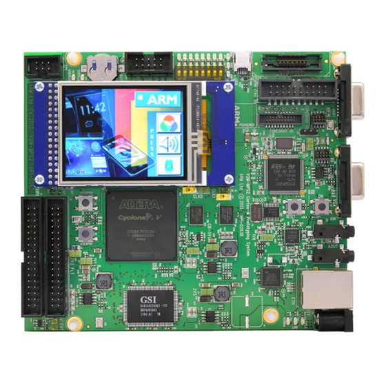
Page 17: Location Of Components On The Mps2 Fpga Prototyping Board
1 Introduction 1.3 Location of components on the MPS2 FPGA Prototyping Board Location of components on the MPS2 FPGA Prototyping Board The following figure shows the upper face of the MPS2 FPGA Prototyping Board. LCD display panel header Expansion connector... - Page 18 1 Introduction 1.3 Location of components on the MPS2 FPGA Prototyping Board 2MB ZBT 2MB ZBT SSRAM SSRAM microSD Card Figure 1-2 Lower face of the MPS2 FPGA Prototyping Board. 100112_0200_09_en Copyright © 2013–2016, 2018–2020 Arm Limited or its affiliates. All 1-18 rights reserved.
-
Page 19: Location Of Components On The Mps2+ Fpga Prototyping Board
1 Introduction 1.4 Location of components on the MPS2+ FPGA Prototyping Board Location of components on the MPS2+ FPGA Prototyping Board The following figure shows the upper face of the MPS2+ FPGA Prototyping Board. LCD display panel header Expansion connector... - Page 20 1 Introduction 1.4 Location of components on the MPS2+ FPGA Prototyping Board 2MB ZBT 2MB ZBT SSRAM SSRAM microSD Card Figure 1-4 Lower face of the MPS2+ FPGA Prototyping Board. 100112_0200_09_en Copyright © 2013–2016, 2018–2020 Arm Limited or its affiliates. All 1-20 rights reserved.
- Page 21 Chapter 2 Hardware Description This chapter describes the MPS2 and MPS2+ board hardware. It contains the following sections: • 2.1 Overview of the MPS2 and MPS2+ hardware on page 2-22. • 2.2 Clocks on page 2-25. • 2.3 Powerup, powerdown, and resets on page 2-27.
-
Page 22: Overview Of The Mps2 And Mps2+ Hardware
2 Hardware Description 2.1 Overview of the MPS2 and MPS2+ hardware Overview of the MPS2 and MPS2+ hardware The hardware infrastructure supports Arm M-class processor evaluation and development, system expansion, and debug interfaces. The following figure shows the high-level hardware infrastructure. - Page 23 2 Hardware Description 2.1 Overview of the MPS2 and MPS2+ hardware The MPS2 and MPS2+ FPGA Prototyping Boards contain the following components and interfaces: • One Altera Cyclone 5CEA7 FPGA on the MPS2 FPGA Prototyping Board: — Speed grade C8.
- Page 24 DAP FPGA debug depends on the design which you implement in the FPGA. — CMSIS-DAP debug accesses the FPGA on the same bus as P‑JTAG/SWD. — The MPS2 and MPS2+ FPGA Prototyping Boards require Motherboard Configuration Controller (MCC) firmware version 2.0.1 or later to support CMSIS-DAP.
-
Page 25: Clocks
MPS2 and MPS2+ FPGA Prototyping Boards provide. The following figure shows the clocks on the MPS2 and MPS2+ FPGA Prototyping Boards. The figure shows two of the clock generators that connect to PLLs inside the FPGA with external loopback to logic inside the FPGA. - Page 26 2 Hardware Description 2.2 Clocks Related information 1.3 Location of components on the MPS2 FPGA Prototyping Board on page 1-17 1.4 Location of components on the MPS2+ FPGA Prototyping Board on page 1-19 3.6.2 generic board configuration file on page 3-57 config.txt...
-
Page 27: Powerup, Powerdown, And Resets
2.3 Powerup, powerdown, and resets Powerup, powerdown, and resets The two reset push buttons generate the reset request signals on the MPS2 and MPS2+ FPGA Prototyping Boards. When you press one of the reset push buttons, Hardware RESET button or ON/OFF/Soft RESET button, the MCC generates appropriate signals to reset the system. -
Page 28: User Expansion Port
Expansion EXP2 Figure 2-4 Board user expansion port The Arduino Adapter Board, available from Arm, supports connectivity to up to two Arduino form factor shield boards. See Application Note AN502 Adapter for Arduino for information on the Arduino Adapter Board. -
Page 29: Usb 2.0 Full Speed Interface
USB 2.0 Full Speed interface The MPS2 and MPS2+ Boards provide one USB 2.0 Full Speed interface that connects to the MCC. In the standby state or during runtime, the USB 2.0 Full Speed interface supports memory access to the microSD card for Drag-and-Drop configuration file editing. -
Page 30: Spi Interface
2 Hardware Description 2.6 SPI interface SPI interface The MPS2 and MPS2+ FPGA Prototyping Boards provides access to a general‑purpose SPI interface from the FPGA. The following figure shows the general‑purpose SPI interface. MPS2/MPS2+ FPGA Prototyping Board FPGA Figure 2-6 MPS2 and MPS2+ FPGA Prototyping Boards general-purpose SPI interface Related information 5.6 SPI connector on page 5-85... -
Page 31: Uart Interface
2 Hardware Description 2.7 UART interface UART interface The MPS2 and MPS2+ FPGA Prototyping Boards provide access to a general‑purpose UART interface from the FPGA in Data Communications Equipment (DCE) configuration. The following figure shows the general‑purpose UART interface. MPS2/MPS2+ FPGA Prototyping Board... -
Page 32: Vga And Clcd Interfaces
2.8 VGA and CLCD interfaces VGA and CLCD interfaces The MPS2 and MPS2+ FPGA Prototyping Boards support VGA and CLCD video output. Overview of the VGA interface The VGA interface consists of a VGA controller in the FPGA, a passive resistor network, and an output VGA port. -
Page 33: Audio Interface
2.9 Audio interface Audio interface The MPS2 and MPS2+ FPGA Prototyping Boards provide a stereo line-level input and a stereo line-level output. The audio interface consists of an audio controller in the FPGA, a low-power audio codec, and input and output stereo audio ports. -
Page 34: Ethernet Interface
Ethernet connector for external connection. Note The MAC/PHY connects to the same 16-bit interface as the 16MB PSRAM external memory. The MPS2 and MPS2+ FPGA Prototyping Boards contain three LEDs that denote Ethernet activity: • LINK LED: —... -
Page 35: User Switches And User Leds
2.11 User switches and user LEDs The MPS2 and MPS2+ FPGA Prototyping Boards provide a user interface that consists of user LEDs and user switches that connect to the FPGA and MCC. The FPGA image and application software define their meaning. -
Page 36: External User Memory
2 Hardware Description 2.12 External user memory 2.12 External user memory The MPS2 and MPS2+ FPGA Prototyping Boards provide external user ZBT SSRAM and PSRAM memory. The external user memory connects to the FPGA and consists of the following: •... - Page 37 SSRAM SSRAM3_ADVnLD SSRAM3_nOE SSRAM3_nCEN SSRAM3_ZZ SSRAM3_MODE SSRAM3_nCE1 Figure 2-12 ZBT SSRAM external user memory interface The following diagram shows the external PSRAM user memory interface. 100112_0200_09_en Copyright © 2013–2016, 2018–2020 Arm Limited or its affiliates. All 2-37 rights reserved. Non-Confidential...
- Page 38 PSRAM 8MB SMB_nOE SMB_nWE SMB_nLB SMB_nUB FPGA PSRAM 8MB SMB_PSRAM_nCE[0] Figure 2-13 PSRAM external user memory interface Related information 2.10 Ethernet interface on page 2-34 100112_0200_09_en Copyright © 2013–2016, 2018–2020 Arm Limited or its affiliates. All 2-38 rights reserved. Non-Confidential...
-
Page 39: Mcc Fpga Serial Interface
If you implement an SCC interface, you must make the following pin assignments in the FPGA: assign CFGCLK CLCD_PDH[13]; assign nCFGRST CLCD_PDH[14]; assign CFGLOAD CLCD_PDH[15]; assign CFGWnR CLCD_PDH[16]; assign CFGDATAIN CLCD_PHD[17]; assign CLCD_PDH[12] CFGDATAOUT; 100112_0200_09_en Copyright © 2013–2016, 2018–2020 Arm Limited or its affiliates. All 2-39 rights reserved. Non-Confidential... - Page 40 ® ® file that implements these registers. Note If the FPGA does not implement an SCC interface, Arm recommends that you tie off the CFGDATAOUT and nRSTREQ signals as follows: • Tie the CFGDATAOUT signal from the FPGA LOW. •...
- Page 41 -500ns Related information 2.11 User switches and user LEDs on page 2-35 4.3 Register summary on page 4-62 4.4 SCC register descriptions on page 4-63 100112_0200_09_en Copyright © 2013–2016, 2018–2020 Arm Limited or its affiliates. All 2-41 rights reserved. Non-Confidential...
-
Page 42: Power
Arm supplies with the board. Arm supplies an external power supply unit which converts mains power to 12V DC which connects to the 12V connector on the board. The unit accepts mains power in the range 110V AC to 240V AC. -
Page 43: Debug And Trace
2.15 Debug and trace 2.15 Debug and trace This section describes the debug and trace systems on the MPS2 and MPS2+ FPGA Prototyping Boards. This section contains the following subsections: • 2.15.1 Overview of FPGA debug and trace systems on page 2-43. - Page 44 FPGA. Related information 1.3 Location of components on the MPS2 FPGA Prototyping Board on page 1-17 1.4 Location of components on the MPS2+ FPGA Prototyping Board on page 1-19 5.1.1 JTAG 14 connector on page 5-75 100112_0200_09_en Copyright ©...
- Page 45 5.1.5 MICTOR 38 connector on page 5-78 2.15.4 4-bit Trace The CoreSight 20 connector supports 4-bit Trace on the MPS2 and MPS2+ FPGA Prototyping Boards. The availability of 4-bit Trace depends on the design which you implement in the FPGA. Related information 1.3 Location of components on the MPS2 FPGA Prototyping Board on page 1-17...
- Page 46 MCC implements CMSIS-DAP which runs over JTAG connection to the debug access port in the FPGA. The availability of CMSIS-DAP depends on the design that you implement in the FPGA. The MPS2 and MPS2+ FPGA Prototyping Boards require Motherboard Configuration Controller (MCC) software version 2.0.1 or later to support CMSIS-DAP.
-
Page 47: Minimum Design Settings For Board Operation
2.16 Minimum design settings for board operation You must implement a minimum amount of RTL in the FPGA for theMPS2 or MPS2+ FPGA Prototyping Board to operate correctly. You must tie off the following FPGA signals to generate the minimum RTL in the FPGA for correct operation: 1. -
Page 48: Configuration
Chapter 3 Configuration This chapter describes the powerup and configuration process of the MPS2 and MPS2+ FPGA Prototyping Boards. It contains the following sections: • 3.1 Overview of the configuration process on page 3-49. • 3.2 Remote USB operation on page 3-51. -
Page 49: Overview Of The Configuration Process
3.1 Overview of the configuration process Overview of the configuration process The MCC, in association with the microSD card, configures the MPS2 and MPS2+ FPGA Prototyping Boards during powerup or reset. When the configuration process starts after application of power or a press of one of the RESET buttons, the configuration process completes without further intervention from the user. - Page 50 3 Configuration 3.1 Overview of the configuration process Related information 2.5 USB 2.0 Full Speed interface on page 2-29 100112_0200_09_en Copyright © 2013–2016, 2018–2020 Arm Limited or its affiliates. All 3-50 rights reserved. Non-Confidential...
-
Page 51: Remote Usb Operation
"bmqjfe". shutdown.txt Related information 1.3 Location of components on the MPS2 FPGA Prototyping Board on page 1-17 1.4 Location of components on the MPS2+ FPGA Prototyping Board on page 1-19 2.5 USB 2.0 Full Speed interface on page 2-29 5.4 USB 2.0 connector on page 5-83... -
Page 52: Configuration System
3 Configuration 3.3 Configuration system Configuration system The MPS2 and MPS2+ FPGA Prototyping Boards provide hardware infrastructure to enable board configuration during powerup or reset. The following diagram shows the board configuration system. MPS2/MPS2+ FPGA Prototyping Board Configuration microSD card... -
Page 53: Powerup And Configuration Process
3.4 Powerup and configuration process Powerup and configuration process The power push buttons and configuration files control the sequence of events of the MPS2 and MPS2+ board powerup and configuration process. The following figure shows the powerup and configuration process. - Page 54 3.6.3 Contents of the MB directory on page 3-57 3.6.4 Contents of the SOFTWARE directory on page 3-58 3.6.1 Overview of configuration files and microSD card directory structure on page 3-56 100112_0200_09_en Copyright © 2013–2016, 2018–2020 Arm Limited or its affiliates. All 3-54 rights reserved. Non-Confidential...
-
Page 55: Reset Push Buttons
3.5 Reset push buttons Reset push buttons The MPS2 and MPS2+ FPGA Prototyping Boards provide two push buttons which initiate reset and configuration. The two reset push buttons are the ON/OFF/Soft RESET and the Hardware RESET buttons. This section describes the use and functions of these push buttons. -
Page 56: Configuration Files
3 Configuration 3.6 Configuration files Configuration files This section describes the MPS2 and MPS2+ board configuration files in the microSD card which control the board powerup and configuration process. This section contains the following subsections: • 3.6.1 Overview of configuration files and microSD card directory structure on page 3-56. - Page 57 3.6.4 Contents of the SOFTWARE directory on page 3-58 3.6.2 generic board configuration file config.txt You can use the MPS2 or MPS2+ FPGA Prototyping Board USB 2.0 Full Speed port to update the generic configuration file from your workstation to the root directory of the microSD card. config.txt The following example shows a configuration file that you can load into the configuration flash memory.
- Page 58 3 Configuration 3.6 Configuration files The following example shows a typical MPS2 or MPS2+ FPGA Prototyping Board application note file. .txt BOARD: HBI0263 TITLE: Application Note File [FPGAS] TOTALFPGAS: 1 ;Total Number of FPGAS (Max : 1) F0FILE: an385_v2.rbf ;FPGA0 Filename F0MODE: FPGA ;FPGA0 Programming Mode...
- Page 59 Chapter 4 Programmers Model This chapter describes the programmers model of the MPS2 and MPS2+ FPGA Prototyping Boards. It contains the following sections: • 4.1 About this programmers model on page 4-60. • 4.2 Memory map on page 4-61. •...
-
Page 60: About This Programmers Model
— Ignore undefined register bits on reads. — All register bits are reset to a logic 0 by a system or powerup reset. — Table 4-1 MPS2 and MPS2+ SCC register summary on page 4-62 describes register access type as follows: RW: Read and write. -
Page 61: Memory Map
4.2 Memory map Memory map The image that you load into the FPGA on the MPS2 or MPS2+ FPGA Prototyping Board determines the board memory map. See the relevant SMM Application Note for an example memory map for the board. -
Page 62: Register Summary
4 Programmers Model 4.3 Register summary Register summary This section summarizes the MPS2 and MPS2+ SCC registers and system configuration registers characteristics. The following table shows the registers in offset order from the base memory address. Table 4-1 MPS2 and MPS2+ SCC register summary... -
Page 63: Scc Register Descriptions
4.4.1 Overview of SCC registers The MCC on the MPS2 or MPS2+ FPGA Prototyping Board writes to the SCC registers in the FPGA at powerup with the values that the configuration board file defines. During runtime, the MCC polls the LED and switch values to ensure that they match the SCC_CFG1 and SCC_CFG2 register values. - Page 64 SCC_CFG1 Register The SCC_CFG1 Register characteristics are: Purpose Controls the USER LEDS on the MPS2 and MPS2+ FPGA Prototyping Boards. The MCC polls this SCC register in the FPGA and updates the appropriate LEDs. Usage constraints There are no usage constraints.
- Page 65 4 Programmers Model 4.4 SCC register descriptions Purpose Determines the state of the eight user switches on the MPS2 and MPS2+ FPGA Prototyping Boards. The MCC polls the switches and updates this SCC register in the FPGA. Usage constraints The SCC_CFG3 Register is read-only.
- Page 66 DLL, contributes to the value of bit[0]. BIT[23:16] DLL_LOCKED[7:0] These bits indicate the lock statuses of the individual DLLs: 0b0 DLL unlocked. • • 0b1 DLL locked. 100112_0200_09_en Copyright © 2013–2016, 2018–2020 Arm Limited or its affiliates. All 4-66 rights reserved. Non-Confidential...
- Page 67 This bit indicates whether the system supports the SCC_LOCK_READ command. [7:0] CFGREGNUM These bits indicate the number of user registers you can define. The maximum number is eight. 100112_0200_09_en Copyright © 2013–2016, 2018–2020 Arm Limited or its affiliates. All 4-67 rights reserved. Non-Confidential...
- Page 68 The SCC_ID Register characteristics are: Purpose The MCC reads this register and uses the information to determine information about the design in the FPGA that you can read through the MPS2 or MPS2+ FPGA Prototyping Board SYS_CFG interface. Usage constraints The SCC_ID Register is Read-only.
- Page 69 4 Programmers Model 4.4 SCC register descriptions Related information 2.13 MCC FPGA serial interface on page 2-39 100112_0200_09_en Copyright © 2013–2016, 2018–2020 Arm Limited or its affiliates. All 4-69 rights reserved. Non-Confidential...
-
Page 70: System Configuration Registers
FPGA writes and reads configuration information to and from peripherals on the MPS2 or MPS2+ FPGA Prototyping Board. The following block of example pseudocode shows a write operation to write 24MHz to clock generator //Write frequency value to the user data out register. - Page 71 The MCC writes data to the SYS_CFGDATA_RTN Register during a read operation. This data represents the value that the addressed MPS2 or MPS2+ FPGA Prototyping Board component returns as a result of the read operation, for example, a clock generator frequency.
- Page 72 Selects device to write to or read from: 0x000 Clock generator 0 • 0x001 Clock generator 1 • • 0x002 Clock generator 2 Related information 4.3 Register summary on page 4-62 100112_0200_09_en Copyright © 2013–2016, 2018–2020 Arm Limited or its affiliates. All 4-72 rights reserved. Non-Confidential...
- Page 73 The SYS_CFGSTAT Register characteristics are: Purpose The SYS_CFGSTAT Register contains system configuration status information about read and write operations between the application software in the FPGA and the MPS2 or MPS2+ Board board peripherals. Usage constraints The SYS_CFGSTAT Register is read-only.
-
Page 74: Chapter 5 Signal Descriptions
Chapter 5 Signal Descriptions This chapter describes the signals present at the interface connectors of the MPS2 and MPS2+ FPGA Prototyping Boards. It contains the following sections: • 5.1 Debug connectors on page 5-75. • 5.2 Expansion connectors on page 5-80. -
Page 75: Debug Connectors
FPGA and debug your design. The JTAG 14 connector connects to general‑purpose pins on the FPGA. The availability of F-JTAG depends on the design which you implement in the FPGA. The MPS2 and MPS2+ FPGA Prototyping Boards label this connector as FJTAG. - Page 76 The connector also supports SWD. The JTAG 20 connector connects to general‑purpose pins on the FPGA. The availability of P-JTAG or SWD depends on the design which you implement in the FPGA. The MPS2 and MPS2+ FPGA Prototyping Boards label this connector as PJTAG.
- Page 77 The CoreSight 20 connector connects to general‑purpose pins on the FPGA. The availability of P-JTAG, SWD, or 4-bit Trace depends on the design which you implement in the FPGA. The MPS2 and MPS2+ FPGA Prototyping Boards label this connector as PJTAG.
- Page 78 The MICTOR 38 connector connects to general‑purpose pins on the FPGA. The availability of P‑JTAG, SWD, and 16-bit Trace depends on the design which you implement in the FPGA. The MPS2 and MPS2+ FPGA Prototyping Boards label this connector as PJTAG/TRACE.
- Page 79 2.15.5 16-bit Trace on page 2-45 2.15.6 Serial Wire Debug on page 2-45 1.3 Location of components on the MPS2 FPGA Prototyping Board on page 1-17 1.4 Location of components on the MPS2+ FPGA Prototyping Board on page 1-19 100112_0200_09_en Copyright ©...
-
Page 80: Expansion Connectors
Pins 9, 13, 14, and 25 of connector EXP1 have source series terminating resistors. These resistors help to maintain the integrity of high slew-rate signals. Arm recommends these pins for use as clock outputs or sensitive data outputs in preference to other pins. - Page 81 Pins 9, 10, 13, 22 and 32 of connector EXP2 have source series termination resistors. These resistors help to maintain the integrity of high-slew rate signals: — Arm recommends pins 9, 10, 13 and 32 for use as clock outputs or sensitive data outputs in preference to other pins.
-
Page 82: Clcd Connector
5 Signal Descriptions 5.3 CLCD connector CLCD connector The MPS2 and MPS2+ FPGA Prototyping Boards provide a female IDC connector that supports CLCD. The following figure shows the CLCD connector. Figure 5-7 CLCD connector Note A mark on the board indicates pin 1. -
Page 83: Usb 2.0 Connector
5.4 USB 2.0 connector USB 2.0 connector The MPS2 and MPS2+ FPGA Prototyping Boards provide one USB 2.0 mini-B connector that provides a USB 2.0 Full Speed port. This port supports configuration file editing in the microSD, virtual UART access to the FPGA, and CMSIS-DAP FPGA debug. -
Page 84: Uart Connector
5 Signal Descriptions 5.5 UART connector UART connector The MPS2 and MPS2+ FPGA Prototyping Boards provide one general‑purpose female UART connector that supports access to the FPGA. The general‑purpose UART connector connects through a level-shifter to the FPGA. The meaning of the UART signals depends on the design which you implement in the FPGA. -
Page 85: Spi Connector
5 Signal Descriptions 5.6 SPI connector SPI connector The MPS2 and MPS2+ FPGA Prototyping Boards provide one general‑purpose SPI connector that supports access to the FPGA. The general‑purpose SPI connector connects to the FPGA. The meaning of the SPI signals depends on the design which you implement in the FPGA. -
Page 86: Vga Connector
5 Signal Descriptions 5.7 VGA connector VGA connector The MPS2 and MPS2+ FPGA Prototyping Boards provide one VGA connector that supports VGA and CLCD output. The VGA connector connects to the VGA controller which connects to general‑purpose pins on the FPGA. -
Page 87: Audio Connectors
5.8 Audio connectors Audio connectors The MPS2 and MPS2+ FPGA Prototyping Boards each provide two 3.5mm stereo jack connectors that connect to a low-power stereo audio codec. The two connectors provide an independent line-level stereo input and an independent line-level stereo output. -
Page 88: Ethernet Connector
The MPS2 and MPS2+ FPGA Prototyping Boards provide one 100Mb/s Ethernet connector. The Ethernet connector connects to the MAC/PHY on the MPS2 and MPS2+ FPGA Prototyping Boards. The MAC/PHY connects to general‑purpose pins on the FPGA. The availability of the Ethernet function depends on the design which you implement in the FPGA. -
Page 89: Power Connector
5.10 12V power connector 5.10 12V power connector The MPS2 and MPS2+ FPGA Prototyping Boards each provide a Thru-hole DC power jack for connecting external power to the board. Connect the external mains power supply unit, which Arm supplies, to the power jack. -
Page 90: Appendix A Specifications
Appendix A Specifications This chapter contains the electrical specification of the MPS2 and MPS2+ FPGA Prototyping Boards and FPGAs. It contains the following section: • A.1 Electrical specification on page Appx-A-91. 100112_0200_09_en Copyright © 2013–2016, 2018–2020 Arm Limited or its affiliates. All Appx-A-90 rights reserved. -
Page 91: Electrical Specification
The following table shows the power available for each power domain, or group of power domains, of the FPGA. Note This table applies to both the Altera Cyclone 5CEA7 FPGA on the MPS2 FPGA Prototyping Board and to the Altera Cyclone 5CEA9 FPGA on the MPS2+ FPGA Prototyping Board. Table A-1 Available FPGA current... -
Page 92: Appendix B Revisions
Appendix B Revisions This chapter describes the technical changes between released issues of this book. It contains the following section: • B.1 Revisions on page Appx-B-93. 100112_0200_09_en Copyright © 2013–2016, 2018–2020 Arm Limited or its affiliates. All Appx-B-92 rights reserved. Non-Confidential... - Page 93 Added the MPS2+ FPGA Prototyping Board so the All board 1.3 Location of components on the MPS2 FPGA document now describes both the MPS2 and MPS2+ FPGA revisions. Prototyping Board on page 1-17 Prototyping Boards. The additional references now include 1.4 Location of components on the MPS2+ FPGA...
- Page 94 3 of the firmware. revisions. Table B-10 Differences between issue 100112-0200-08 and issue 100112-0200-09 Change Location Affects Updated CE Conformance Notice. All board Conformance Notices on page revisions. 100112_0200_09_en Copyright © 2013–2016, 2018–2020 Arm Limited or its affiliates. All Appx-B-94 rights reserved. Non-Confidential...
Need help?
Do you have a question about the MPS2 and is the answer not in the manual?
Questions and answers