Table of Contents
Advertisement
Quick Links
Advertisement
Table of Contents

Related Manuals for Nvidia Jetson TX2 NX


Summary of Contents for Nvidia Jetson TX2 NX
- Page 1 NVIDIA Jetson TX2 NX Product Design Guide DG-10141-001_v1.1 September 2021...
- Page 2 MOD_SLEEP* in Table 5-1 “Jetson TX2 NX Power and System Pin Descriptions” Updated SHUTDOWN_REQ* pull-up and MOD_SLEEP* • usage in Figure 5-1 “Jetson TX2 NX Power and Control Block Diagram” Replaced much of the existing text with more detail per •...
-
Page 3: Table Of Contents
Chapter 1. Introduction ................... 1 References .......................... 1 Abbreviations and Definitions .................... 2 Chapter 2. Jetson TX2 NX ..................4 Chapter 3. Developer Kit Feature Considerations ..........7 Button Power MCU ......................7 USB SuperSpeed Hub ......................8 Power over Ethernet ......................8 TI TXB0108 Level Shifters .................... - Page 4 Chapter 13. Unused Interface Terminations ............69 13.1 Unused Multi-purpose Standard CMPS Pad Interfaces ..........69 Chapter 14. Jetson TX2 NX Pin Descriptions and Design Checklist ....... 70 Chapter 15. General Routing Guidelines ..............71 15.1 Signal Name Conventions ....................71 15.2 Routing Guideline Format ....................
- Page 5 List of Figures Figure 2-1. Jetson TX2 NX Block Diagram ................5 Figure 4-1. Jetson TX2 NX Module Installed in SODIMM Connector ........9 Figure 4-2. Module to Connector Assembly Diagram ............10 Figure 5-1. Jetson TX2 NX Power and Control Block Diagram ..........12 Figure 5-2.
- Page 6 Basic SPI Master and Slave Connections ............61 Figure 11-4. SPI Topologies ...................... 61 Figure 11-5. Jetson TX2 NX CAN Connections ................ 62 Figure 11-6. Jetson TX2 NX Fan Connections ................63 Figure 11-7. Jetson TX2 NX UART Connections ..............64 Figure 11-8.
- Page 7 Jetson TX2 NX USB 2.0 Pin Descriptions ............16 Table 6-2. Jetson TX2 NX USB 3.0 and PCIe Pin Descriptions ..........16 Table 6-3. Jetson TX2 NX USB 3.0 and PCIe Lane Mapping Configurations ...... 17 Table 6-4. USB 2.0 Interface Signal Routing Requirements ..........19 Table 6-5.
- Page 8 Table 10-3. Audio Signal Connections ..................56 Table 11-1. Jetson TX2 NX I2C Pin Description ..............57 Table 11-2. I2C Interface Signal Routing Requirements ............59 Table 11-3. I2C Signal Connections ..................59 Table 11-4. Jetson TX2 NX SPI Pin Description ..............60 Table 11-5.
-
Page 9: Chapter 1. Introduction
This design guide provides detailed information on the capabilities of the hardware module, which may differ from supported configurations by provided software. Refer to software release documentation for information on supported capabilities. Note: Most of the interface usage noted in this design guide is based on the NVIDIA Jetson ®... -
Page 10: Abbreviations And Definitions
Mobile Industry Processor Interface Millimeter PCIe Peripheral Component Interconnect Express interface Pulse Code Modulation Physical Interface (i.e. USB PHY) Pico-Seconds Power Management Unit RJ45 8P8C modular connector used in Ethernet and other data links NVIDIA Jetson TX2 NX DG-10141-001_v1.1 | 2... - Page 11 Real Time Clock SD Card Secure Digital Card SDIO Secure Digital I/O Interface Single-Ended SODIMM Small Outline Dual In-line Memory Module Serial Peripheral Interface TMDS Transition-minimized differential signaling UART Universal Asynchronous Receiver-Transmitter Universal Serial Bus NVIDIA Jetson TX2 NX DG-10141-001_v1.1 | 3...
-
Page 12: Chapter 2. Jetson Tx2 Nx
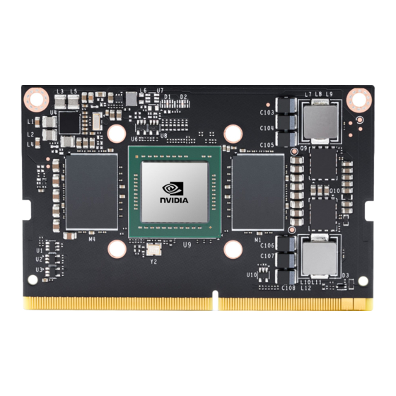
Chapter 2. Jetson TX2 NX The Jetson TX2 NX module resides at the center of the embedded system solution and includes the following: Power (PMIC/Regulators, etc.) DRAM (LPDDR4) eMMC Gigabit Ethernet Controller Power Monitor In addition, a wide range of interfaces are available at the main connector for use on the carrier board as shown Table 2-1 and Figure 2-1. -
Page 13: Figure 2-1. Jetson Tx2 Nx Block Diagram
CAM MCLK x2 UART x3 Misc. Clocks 2x PWM 3x Table 2-2 lists the 260-pin SODIMM description for the Jetson TX2 NX connector. Table 2-2. Jetson TX2 NX Connector Pinout Matrix Module Signal Name Pin # Pin # Module Signal Name... - Page 14 VDD IN VDD IN PCIE0 RX0 N Legend Ground Power Reserved - must be left unconnected Note: Refer to the Jetson TX2 NX pin description spreadsheet attached to this design guide for more details. NVIDIA Jetson TX2 NX DG-10141-001_v1.1 | 6...
-
Page 15: Chapter 3. Developer Kit Feature Considerations
Chapter 3. Developer Kit Feature Considerations The Jetson TX2 NX module is compatible with the NVIDIA Jetson Xavier NX Developer Kit. The Jetson Xavier NX Developer Kit carrier board design files are provided as a reference design. This chapter describes details necessary for designers to know to replicate certain features if desired. -
Page 16: Usb Superspeed Hub
The ID EEPROM (P3509 - U17) is a feature that is used for NVIDIA internal purposes, but not useful on a custom design. A similar function may be desired for a custom design, but the NVIDIA software will not interact with these devices and the I2C address used by the developer kit carrier board ID EEPROM on the I2C2 interface (7’h57) should be avoided. -
Page 17: Chapter 4. Module Connector
Jetson TX2 NX modules connect to the carrier board using a 260-pin SODIMM connector. The mating connector used on the developer kit carrier board is listed in the Jetson TX2 NX Supported Components List (SCL). This connector is a DDR4 SODIMM, 260-pin, right-angle, standard key type. -
Page 18: Module Installation And Removal
The developer kit (shown in Figure 4 2) uses a standoff and screws to secure the module to the system/base- board. Figure 4-2. Module to Connector Assembly Diagram To remove the Jetson TX2 NX module correctly, follow the reverse of the installation sequence. NVIDIA Jetson TX2 NX DG-10141-001_v1.1 | 10... -
Page 19: Chapter 5. Power
VDD_IN NX Data Sheet for supply tolerance and maximum current). CAUTION: Jetson TX2 NX is not hot-pluggable. When installing the module, the main power supply should not be connected. Before removing the module, the main power supply (to VDD_IN pins) must be disconnected and allowed to discharge below 0.6V. -
Page 20: Power Supply And Sequencing
1.8V Notes: In the Type/Dir column, Output is from Jetson TX2 NX. Input is to Jetson TX2 NX. Bidir is for Bidirectional signals. The directions for FORCE_RECOVERY* and SLEEP/WAKE* signals are true when used for those functions. Otherwise as GPIOs, the direction is bidirectional. - Page 21 POWER_EN brought down as well. Using to power the system OFF is an option, but POWER_EN must be asserted soon after. SHUTDOWN_REQ* NVIDIA Jetson TX2 NX DG-10141-001_v1.1 | 13...
-
Page 22: Power Sequencing
DOES NOT limit reverse current. 5.1.2 Power Sequencing The following figures show the power sequencing for the Jetson TX2 NX module. Figure 5-3. Power Up Sequence (No Power Button – Auto Power-On) VDD_IN... -
Page 23: Figure 5-4. Power-Up Sequence (With Power Button)
3.0V T > 10mS SHUTDOWN_REQ* POWER_EN T < 10uS Note: must always be serviced by the carrier board to toggle from SHUTDOWN_REQ* POWER_EN high to low, even in cases of sudden power loss. NVIDIA Jetson TX2 NX DG-10141-001_v1.1 | 15... -
Page 24: Chapter 6. Usb And Pci Express
Notes: In the Type/Dir column, Output is from Jetson TX2 NX. Input is to Jetson TX2 NX. Bidir is for Bidirectional signals. The direction of GPIO00 is true when used for this function. Otherwise as a GPIO, the direction is bidirectional. -
Page 25: Table 6-3. Jetson Tx2 Nx Usb 3.0 And Pcie Lane Mapping Configurations
USBSS_TX_P USBSS_TX_P PEX_TX1P Notes: In the Type/Dir column, Output is from Jetson TX2 NX. Input is to Jetson TX2 NX. Bidir is for Bidirectional signals. Table 6-3 lists the mapping options for Jetson TX2 NX. Table 6-3. Jetson TX2 NX USB 3.0 and PCIe Lane Mapping Configurations... -
Page 26: Usb
TPD4E 05U06 Notes: 1. AC capacitors should be located close to either the USB connector, or the Jetson TX2 NX pins. 2. For USB 3.0 IF shown above ( ), AC caps are required on the TX lines. If routed USBSS_TX/RX directly to a peripheral, AC caps are needed on the peripheral TX lines as well. -
Page 27: Usb 2.0 Design Guidelines
If routing on the same layer, strongly recommend not interleaving TX and RX lanes If it is necessary to have interleaved routing in breakout, all the inter-pair spacing should follow the rule of inter-SNEXT NVIDIA Jetson TX2 NX DG-10141-001_v1.1 | 19... - Page 28 (IL and resonance dip check). Preferred device Type: Texas Instruments TPD4I05U06. Optional. Place ESD component near connector Max junction capacitance (IO to GND) Location (max distance to connector) 8 (53) mm (ps) NVIDIA Jetson TX2 NX DG-10141-001_v1.1 | 20...
-
Page 29: Figure 6-2. Il/Next Plot
3. Place GND vias as symmetrically as possible to data pair vias. The following figures show the USB 3.0 interface signal routing requirements. Figure 6-2. IL/NEXT Plot Figure 6-3. Trace Spacing for TX/RX Non-Interleaving NVIDIA Jetson TX2 NX DG-10141-001_v1.1 | 21... -
Page 30: Common Usb Routing Guidelines
If routing to USB device or USB connector includes a flex or 2nd PCB, the total routing including all PCBs/flexes must be used for the max trace and skew calculations. Keep critical USB related traces away from other signal traces or unrelated power traces/areas or power supply components. NVIDIA Jetson TX2 NX DG-10141-001_v1.1 | 22... -
Page 31: Pcie
(USB 3.0 Port #0) devices on the PCB. peripheral TX lines. ESD protection near connector if required. PCIe Jetson TX2 NX brings two PCIe interfaces to the module pins. One x1 and one x2 interface. NVIDIA Jetson TX2 NX DG-10141-001_v1.1 | 23... -
Page 32: Figure 6-7. Example Pcie Connections
2. See design guidelines for correct AC capacitor values. 3. The PCIe clock outputs comply to the PCIe CEM specification “REFCLK DC Specifications and AC Timing Requirements.” The clocks are HCSL compatible as are the RX/TX signals. NVIDIA Jetson TX2 NX DG-10141-001_v1.1 | 24... -
Page 33: Pcie Design Guidelines
Routing signals over antipads Not allowed AC Cap Value (Min/Max) 0.075 / 0.2 Only required for TX when routed to connector Location (max length to adjacent discontinuity) Discontinuity such as edge finger, component pad NVIDIA Jetson TX2 NX DG-10141-001_v1.1 | 25... -
Page 34: Figure 6-8. Ac Cap Voiding
DIFF IN Series 0.1uF capacitors Differential Receive Data Pairs: Connect to RX_N/P pins of PCIe near Jetson TX2 NX pins or connector or TX_N/P pin of PCIe device through AC cap PCIE0_RX0_N/P - Lane 0 device if device on main according to supported configuration. -
Page 35: Gigabit Ethernet
GbE Transformer Data 2 GBE_MDI2_P − GBE_MDI3_N − GbE Transformer Data 3 GBE_MDI3_P − Notes: In the Type/Dir column, Output is from Jetson TX2 NX. Input is to Jetson TX2 NX. Bidir is for Bidirectional signals. NVIDIA Jetson TX2 NX DG-10141-001_v1.1 | 27... -
Page 36: Figure 6-9. Jetson Tx2 Nx Ethernet Connections
USB and PCI Express Figure 6-9. Jetson TX2 NX Ethernet Connections Jetson Tegra SDMMC2_HV EQOS_TXC Ethernet EQOS_TD0 EQOS_TD1 EQOS_TD2 GBE_MDI0_P EQOS_TD3 GBE_MDI0_N EQOS_TX_CTL GBE_MDI1_P GBE_MDI1_N EQOS_RXC GBE_MDI2_P EQOS_RD0 To Magnetics/ GBE_MDI2_N EQOS_RD1 GBE_MDI3_P RJ45 Connector EQOS_RD2 GBE_MDI3_N EQOS_RD3 EQOS_RX_CTL GBE_LED_ACT... -
Page 37: Table 6-12. Ethernet Mdi Interface Signal Routing Requirements
Gigabit Ethernet MDI IF Pairs: Connect to Magnetics -/+ pins GBE_LED_LINK 110Ω series resistor Gigabit Ethernet Link LED: Connect to green LED on RJ45 connector GBE_LED_ACT 110Ω series resistor Gigabit Ethernet Activity LED: Connect to yellow LED on RJ45 connector NVIDIA Jetson TX2 NX DG-10141-001_v1.1 | 29... -
Page 38: Chapter 7. Display
DSI_A_D0_P DSI_D1_N DSI_A_D1_N Display, DSI data lane 1 Output DSI_D1_P DSI_A_D1_P Note: In the Type/Dir column, Output is from Jetson TX2 NX. Input is to Jetson TX2 NX. Bidir is for Bidirectional signals. NVIDIA Jetson TX2 NX DG-10141-001_v1.1 | 30... -
Page 39: Mipi Dsi And Csi Design Guidelines
Max PCB breakout length Insertion Loss 1 Gbps 1.5 Gbps 2.5 Gbps 1.92 Max trace delay 1 Gbps 421 (2526) mm (ps) 1.5 Gbps 319 (1913) 2.5 Gbps 150 (900) Max intra-pair skew NVIDIA Jetson TX2 NX DG-10141-001_v1.1 | 31... -
Page 40: Mipi Dsi And Csi Connection Guidelines
Jetson modules include two interfaces (DP0 and DP1). Both support eDP / DP or HDMI. See Jetson TX2 NX Data Sheet for the maximum resolution supported. Table 7-5. Jetson TX2 NX eDP and DP Pin Description Usage on DevKit Pin # Module Pin Name... -
Page 41: Edp And Dp
Open Drain, 3.3V Note: In the Type/Dir column, Output is from Jetson TX2 NX. Input is to Jetson TX2 NX. Bidir is for Bidirectional signals. A standard eDP 1.4/DP 1.2a or HDMI V2.0a/b interface is supported. These share the same set of interface pins, so either DisplayPort or HDMI can be supported natively. -
Page 42: Edp And Dp Routing Guidelines
LANE_0P TPD4E 05U06 Notes: Level shifter required on DPx_HPD to avoid the pin from being driven when Jetson TX2 NX is • off. The level shifter must be non-inverting (preserve the polarity of the HPD signal from the display). The reference design uses a BJT level shifter and a resistor divider is needed. See the reference design if a similar approach will be used. -
Page 43: Table 7-7. Edp/Dp Main Link Signal Routing Requirements Including Dp_Aux
Max PCB via dist. from connector RBR/HBR No requirement mm (in) HBR2 7.63 (0.3) Max trace length/delay from Jetson TX2 NX TX to 175ps/inch assumption for stripline, connector 150ps/inch for microstrip. RBR/HBR (Stripline / Microstrip) 215 (1138)/215 (975) mm (ps) - Page 44 3. Do not perform length matching within breakout region. Recommend doing trace length matching to <1ps before vias or any discontinuity to minimize common mode conversion. 4. The average of the differential signals is used for length matching. NVIDIA Jetson TX2 NX DG-10141-001_v1.1 | 36...
-
Page 45: Figure 7-4. S-Parameter
From module pin: 10kΩ pull-up to 1.8V, level shifter eDP/DP: Hot Plug Detect: Connect to HPD pin on and 100kΩ pulldown on connector side of shifter and display connector through level shifter. ESD to GND. NVIDIA Jetson TX2 NX DG-10141-001_v1.1 | 37... -
Page 46: Hdmi
The DP1_TXx pads are native DP pads and require series AC capacitors (ACCAP) and pull-downs (RPD) to be HDMI compliant. The 499Ω, 1% pull-downs must be disabled when Jetson TX2 NX is off or in sleep mode to meet the HDMI VOFF requirement. The enable to the FET, enables the pull-downs when the HDMI interface is to be used. -
Page 47: Hdmi Routing Guidelines
< 250ps FEXT (PSFEXT) <= -50 dB at DC PSNEXT is derived from an algebraic summation of the individual NEXT <= -40 dB at 3GHz effects on each pair by the other pairs NVIDIA Jetson TX2 NX DG-10141-001_v1.1 | 39... - Page 48 The main route via dimensions should comply with the via structure rules (See via section) See Figure 7-8 For the connector pin vias, follow the rules for the connector pin vias (See via section) NVIDIA Jetson TX2 NX DG-10141-001_v1.1 | 40...
- Page 49 Vlow test and HF1-9 TDR test Location After all components and before HDMI connector Void GND/PWR void under/above the R device is needed. Void size = SMT area + 1x dielectric height keepout distance. NVIDIA Jetson TX2 NX DG-10141-001_v1.1 | 41...
-
Page 50: Figure 7-9. Il And Fext Plot
4. If routing includes a flex or 2nd PCB, the max trace delay and skew calculations must include all the PCBs/flex routing. Solutions with flex/2nd PCB may not achieve maximum frequency operation. The following figures show the HDMI interface signal routing requirements. Figure 7-9. IL and FEXT Plot Figure 7-10. TDR Plot NVIDIA Jetson TX2 NX DG-10141-001_v1.1 | 42... -
Page 51: Figure 7-11. Hdmi Via Topology
Display Figure 7-11. HDMI Via Topology Figure 7-12. Add-on Components – Top Figure 7-13. Add-on Components – Bottom Figure 7-14. AC Cap Void Figure 7-15. RPD, Chock, FET Placement NVIDIA Jetson TX2 NX DG-10141-001_v1.1 | 43... -
Page 52: Figure 7-16. Esd Footprint
Display Figure 7-16. ESD Footprint Figure 7-17. ESD Void Figure 7-18. SMT Pad Trace Entering Figure 7-19. SMT Pad Trace Between Figure 7-20. Connector Voiding NVIDIA Jetson TX2 NX DG-10141-001_v1.1 | 44... -
Page 53: Table 7-10. Hdmi Signal Connections
Adequate decoupling (0.1uF and 10uF recommended) on HDMI 5V supply to connector: Connect to +5V supply near connector and ESD to GND. on HDMI connector. Note: Any ESD and /or EMI solutions must support targeted modes (frequencies). NVIDIA Jetson TX2 NX DG-10141-001_v1.1 | 45... -
Page 54: Chapter 8. Mipi Csi Video Input
Chapter 8. MIPI CSI Video Input Jetson TX2 NX brings twelve MIPI CSI lanes to the connector. Three quad-lane camera streams or two quad-lane plus two dual-lane camera streams or one quad-lane plus three dual-lane camera streams are supported. Each data lane has a peak bandwidth of up to 2.5 Gbps. -
Page 55: Figure 8-1. 4 Lane Csi Camera Connection Example
Camera, CSI 4 Data 3 CSI4_D3_P CSI_F_D1_P Note: In the Type/Dir column, Output is from Jetson TX2 NX. Input is to Jetson TX2 NX. Bidir is for Bidirectional signals. Table 8-2. Jetson TX2 NX Camera Miscellaneous Pin Description Usage on DevKit... -
Page 56: Figure 8-2. Available Camera Control Pins
CAM0_MCLK EXTPERIPH1_CLK Camera 0 CAM0_PWDN GPIO_CAM1 Clock/Control CAM1_MCLK EXTPERIPH2_CLK Camera 1 CAM1_PWDN GPIO_CAM4 Clock/Control Note: The CAM_I2C interface is connected to the power monitor device on the module which uses I2C address 7’h40. NVIDIA Jetson TX2 NX DG-10141-001_v1.1 | 48... -
Page 57: Figure 8-3. Csi Connection Options
Note: Any EMI/ESD devices must be tuned to minimize impact to signal quality and meet the timing and Vil/Vih requirements at the receiver and maintain signal quality and meet requirements for the frequencies supported by the design. NVIDIA Jetson TX2 NX DG-10141-001_v1.1 | 49... -
Page 58: Csi Design Guidelines
Description CAM_I2C_CLK 2.2kΩ pull-ups VDD_3V3_SYS (on Camera I2C Interface: Connect to I2C SCL and SDA Jetson TX2 NX). See note related to pins of imager. The CAM_I2C interface is connected CAM_I2C_DAT EMI/ESD in Table 8-4. to the power monitor device on the module which uses I2C address 7’h40. -
Page 59: Chapter 9. Sd Card And Sdio
Notes: In the Type/Dir column, Output is from Jetson TX2 NX. Input is to Jetson TX2 NX. Bidir is for Bidirectional signals. The directions for SDMMC_x are true when used for these functions. Otherwise as GPIOs, the directions are bidirectional. -
Page 60: Figure 9-1. Sd Card Connection Example
Max via count Independent of stack-up layers. Depends on stack-up layers. < 3.8 (24) mm (ps) Up to four signal vias can share Via proximity (Signal to reference) 1 GND return via NVIDIA Jetson TX2 NX DG-10141-001_v1.1 | 52... -
Page 61: Table 9-3. Sd Card And Sdio Signal Connections
SD Card / SDIO Clock: Connect to CLK pin of device. SDMMC_CMD SD Card / SDIO Command: Connect to CMD pin of device SDMMC_D[3:0] SD Card / SDIO Data: Connect to Data pins of device NVIDIA Jetson TX2 NX DG-10141-001_v1.1 | 53... -
Page 62: Chapter 10. Audio
Notes: In the Type/Dir column, Output is from Jetson TX2 NX. Input is to Jetson TX2 NX. Bidir is for Bidirectional signals. The directions for pins with I2S functions and GPIO09 are true when used for those functions. Otherwise as GPIOs, the directions are bidirectional. -
Page 63: Figure 10-1. Audio Connections
2) Notes: 1. The Interrupt pin from the audio codec can connect to any available Jetson TX2 NX GPIO. If the pin must be wake-capable, choose one of the GPIOs that supports this function. 2. I2C2 supports 1.8V operation since the interface is pulled to 1.8V through 2.2 kΩ resistors on the module. -
Page 64: Table 10-2. Interface Signal Routing Requirements
GPIO02 (I2S2_DOUT) GPIO12 (I2S3_DOUT) I2S[1:0]_DIN I2S Data Input: Connect to data output pin of audio device. GPIO03 (I2S2_DIN) GPIO10 (I2S3_DIN) GPIO09 (AUD_MCLK) Audio Codec Master Clock: Connect to clock pin of audio codec. NVIDIA Jetson TX2 NX DG-10141-001_v1.1 | 56... -
Page 65: Chapter 11. Miscellaneous Interfaces
General I2C 2 Data. 2.2kΩ pull-up to Open Drain – I2C2_SDA GEN8_I2C_SDA 1.8V on the module. 1.8V Notes: In the Type/Dir column, Output is from Jetson TX2 NX. Input is to Jetson TX2 NX. Bidir is for Bidirectional signals. NVIDIA Jetson TX2 NX DG-10141-001_v1.1 | 57... -
Page 66: I2C Design Guidelines
11.1.1 I2C Design Guidelines Care must be taken to ensure I2C peripherals on same I2C bus connected to Jetson TX2 NX do not have duplicate addresses. Addresses can be in two forms: 7-bit, with the read/write bit removed or 8-bit including the read/write bit. Be sure to compare I2C device addresses using the same form (all 7-bit or all 8-bit format). - Page 67 For I2C interfaces that are pulled up to 1.8V, disable the E_IO_HV option for these pads. For I2C interfaces that are pulled up to 3.3V, enable the E_IO_HV option. The E_IO_HV option is selected in the Pinmux registers. NVIDIA Jetson TX2 NX DG-10141-001_v1.1 | 59...
-
Page 68: Spi
Notes: In the Type/Dir column, Output is from Jetson TX2 NX. Input is to Jetson TX2 NX. Bidir is for Bidirectional signals. The directions for SPI[1:0]x are true when used for those functions. Otherwise as GPIOs, the directions are bidirectional. -
Page 69: Spi Design Guidelines
2x-load star/daisy Max trace length/delay skew from MOSI, MISO and 16 (100) mm (ps) At any point CS to SCK Note: Up to four signal vias can share a single GND return via. NVIDIA Jetson TX2 NX DG-10141-001_v1.1 | 61... -
Page 70: Can
Notes: In the Type/Dir column, Output is from Jetson TX2 NX. Input is to Jetson TX2 NX. Bidir is for Bidirectional signals. The directions for the CAN signals is true when used for that function. Otherwise as GPIOs, the directions are bidirectional. -
Page 71: Uart
Notes: In the Type/Dir column, Output is from Jetson TX2 NX. Input is to Jetson TX2 NX. Bidir is for Bidirectional signals. The directions for GPIO14 and GPIO08 are true when used for those functions. Otherwise as GPIOs, the directions are bidirectional. -
Page 72: Debug
Notes: In the Type/Dir column, Output is from Jetson TX2 NX. Input is to Jetson TX2 NX. Bidir is for Bidirectional signals. The direction for UART2_RXD is true when used for this function. Otherwise as a GPIO, the direction is bidirectional. -
Page 73: Debug Uart
UART #2 Transmit: Connect to RX pin of serial device UART2_RXD If level shifter implemented, 100kΩ to supply UART #2 Receive: Connect to TX pin of serial on the non-Jetson TX2 NX side of the device. device NVIDIA Jetson TX2 NX DG-10141-001_v1.1 | 65... -
Page 74: Chapter 12. Pads
If these signals need the pull-ups during Power-ON, external pull-up resistors should be added. The following list is the affected pins list. These are the Jetson TX2 NX pins on the dual-voltage blocks powered at 1.8V with Power-ON reset default of Internal pull-up enabled. -
Page 75: Pins Pulled And Driven High During Power-On
The Jetson TX2 NX is powered up before the carrier board (See Section 5.1). Table 12-1 lists the pins on Jetson TX2 NX that default to being pulled or driven high. Care must be taken on the carrier board design to ensure that any of these pins that connect to devices on the carrier board (or devices connected to the carrier board) do not cause damage or excessive leakage to those devices. - Page 76 PADS Table 12-2. Pins Pulled High on Module with External Resistors Prior to SYS_RESET_IN* Inactive Jetson TX2 NX Pin Pull-up Supply External Jetson TX2 NX Pin Pull-up Supply External Voltage (V) Voltage (V) Pull-up (kΩ) Pull-up (kΩ) SLEEP/WAKE* PCIE0_CLKREQ* SHUTDOWN_REQ*...
-
Page 77: Chapter 13. Unused Interface Terminations
Unused Multi-purpose Standard CMPS Pad Interfaces The following Jetson TX2 NX pins (and groups of pins) are Tegra X2 MPIO pins that support either special function IOs (SFIO) and/or GPIO capabilities. Any unused pins or portions of pin groups listed in Table 13-1 that are not used can be left unconnected. -
Page 78: Chapter 14. Jetson Tx2 Nx Pin Descriptions And Design Checklist
Descriptions and Design Checklist The Jetson TX2 NX pin description and design checklist are attached to this design guide. To access the attached files, click the Attachment icon on the left-hand toolbar on this PDF (using Adobe Acrobat Reader or Adobe Acrobat). Select the file and use the Tool Bar options (Open, Save) to retrieve the documents. -
Page 79: Chapter 15. General Routing Guidelines
Chapter 15. General Routing Guidelines 15.1 Signal Name Conventions The following conventions are used in describing the signals for Jetson TX2 NX: Signal names use a mnemonic to represent the function of the signal. For example, Secure Digital Interface #3 Command signal is represented as... -
Page 80: Routing Guideline Format
Each interface has different trace impedance requirements and spacing to other traces. It is up to designer to calculate trace width and spacing required to achieve specified SE and Diff impedances. Unless otherwise noted, trace impedance values are ±15%. NVIDIA Jetson TX2 NX DG-10141-001_v1.1 | 72... -
Page 81: General Pcb Routing Guidelines
NX mating connector resides) and any additional routing on a Flex/ secondary PCB segment connected to main PCB. The max length/delay should be from Jetson TX2 NX to the actual connector (i.e. USB, HDMI, etc.) or device (i.e. onboard USB device, Display driver IC, camera imager IC, etc.) -
Page 82: Common High-Speed Interface Requirements
Routing over voids not allowed except void around device ball/pin the signal is routed to. Noise Coupling Keep critical high-speed traces away from other signal traces or unrelated power traces/areas or power supply components NVIDIA Jetson TX2 NX DG-10141-001_v1.1 | 74... -
Page 83: Figure 15-2. Common Mode Choke
General Routing Guidelines The following figures are the common high-speed interface signal routing requirements figures. Figure 15-2. Common Mode Choke Figure 15-3. Serpentine NVIDIA Jetson TX2 NX DG-10141-001_v1.1 | 75... - Page 84 NVIDIA product and may result in additional or different conditions and/or requirements beyond those contained in this document. NVIDIA accepts no liability related to any default, damage, costs, or problem which may be based on or attributable to: (i) the use of the NVIDIA product in any manner that is contrary to this document or (ii) customer product designs.
Need help?
Do you have a question about the Jetson TX2 NX and is the answer not in the manual?
Questions and answers