JVC XV-521BK Service Manual
Hide thumbs
Also See for XV-521BK:
- Instructions manual (52 pages) ,
- Service manual (50 pages) ,
- Instructions manual (52 pages)
Table of Contents
Advertisement
Quick Links
SERVICE MANUAL
XV-521BK/523GD
XV-525BK/421BK
Contents
Safety precautions
Importance administering
point on the safety
Dismantling and assembling
the traverse unit
DVD PLAYER
1-2
1-3
1-4
COPYRIGHT
2000 VICTOR COMPANY OF JAPAN, LTD.
Disassembly method
Precautions for service
Description of major ICs
XV-521BK/523GD
XV-525BK/421BK
Area Suffix
XV-421BK
J
U.S.A
Area Suffix
XV-525BK/523GD
J
U.S.A
Area Suffix
XV-521BK
C
Canada
1-5
1-15
1-16
No.20836
Jun. 2000
Advertisement
Table of Contents

Related Manuals for JVC XV-521BK


Summary of Contents for JVC XV-521BK
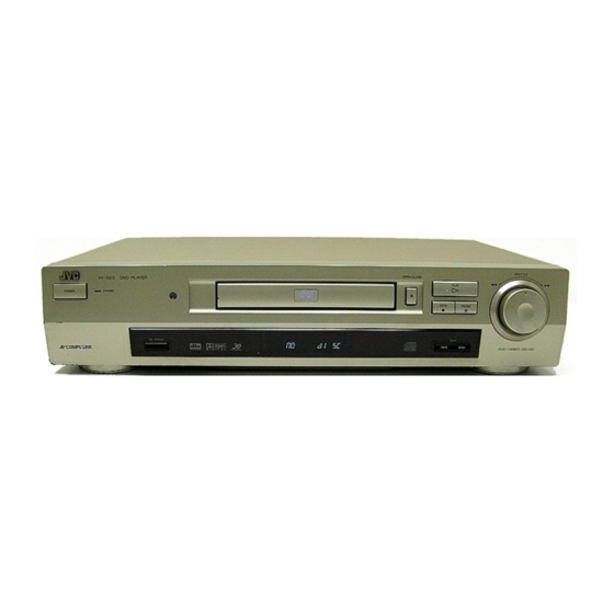
- Page 1 XV-521BK/523GD XV-525BK/421BK SERVICE MANUAL DVD PLAYER XV-521BK/523GD XV-525BK/421BK Area Suffix XV-421BK U.S.A Area Suffix XV-525BK/523GD U.S.A Area Suffix XV-521BK Canada Contents Safety precautions Disassembly method Importance administering Precautions for service 1-15 point on the safety Description of major ICs 1-16...
-
Page 2: Safety Precautions
XV-521BK/523GD/525BK/421BK Safety Precautions 1. This design of this product contains special hardware and many circuits and components specially for safety purposes. For continued protection, no changes should be made to the original design unless authorized in writing by the manufacturer. -
Page 3: Importance Administering Point On The Safety
XV-521BK/523GD/525BK/421BK Importance administering point on the safety F901 For USA and Canada / pour Etats - Unis d' Amerique et Canada Caution: For continued protection against risk of fire, replace only with same type 1.6A/250V for F901. This symbol specifies type of fast operating fuse. -
Page 4: Dismantling And Assembling The Traverse Unit
XV-521BK/523GD/525BK/421BK Dismantling and assembling the traverse unit 1. Notice regarding replacement of optical pickup Electrostatic discharge (ESD), which occurs when static electricity stored in the body, fabric, etc. is discharged, can destroy the laser diode in the traverse unit (optical pickup). Take care to prevent this when performing repairs to the optical pickup or connected devices. -
Page 5: Disassembly Method
XV-521BK/523GD/525BK/421BK Disassembly method Top cover < Main body> Removing the top cover (See Fig.1) Remove the four screws A on both side of the body. Remove the two screws B on the back of the body. Lift up the rear part of the top cover while pulling the lower part of the sides, then detach upward. - Page 6 XV-521BK/523GD/525BK/421BK Removing the fitting (See Fig.3 to 6) Front panel Hole Prior to performing the following procedure, remove the top cover. ATTENTION: To remove the front panel assembly and the DVD mechanism assembly, remove the fitting in advance. by hand Turn over the body.
- Page 7 XV-521BK/523GD/525BK/421BK Removing the front panel assembly (See Fig.7 to 10) DC mechanism assembly Main board AC jack board Prior to performing the following procedure, remove the top cover and the fitting. Disconnect the card wire from connector CN703 on the main board.
- Page 8 XV-521BK/523GD/525BK/421BK Loading tray Removing the DVD mechanism assembly (See Fig.11 to 14) Prior to performing the following procedure, remove the top cover and the front panel assembly. CN101 Disconnect the card wire from connector CN101 on the DVD Servo. DVD Servo Disconnect the harness from connector CN031 on the DVD mechanism assembly.
- Page 9 XV-521BK/523GD/525BK/421BK Removing the AC jack board (See Fig.15 and 16) AC jack board CN951 / CN705 Main board Prior to performing the following procedure, remove the top cover and the front panel assembly. Remove the two screws H attaching the AC jack board.
-
Page 10: Removing The Mainboard
XV-521BK/523GD/525BK/421BK Removing the main board (See Fig.19 and 20) Main board Prior to performing the following procedure, remove the top cover, the front panel assembly, the DVD mechanism assembly, the AC jack board and the DVD Servo. Remove the three screws J attaching the main board. - Page 11 XV-521BK/523GD/525BK/421BK <DVD mechanism> Traverse mechanism unit Spring Removing the traverse mechanism unit (See Fig.1 and 2) Remove the screw A and the spring on the upper side of the loading base assembly. Move the rear part of the traverse mechanism unit upward and pull backward to release the two joints a with the base chassis.
- Page 12 XV-521BK/523GD/525BK/421BK Pickup unit Removing the pickup (See Fig.5 to 9) It is not necessary to remove the traverse mechanism unit. Flexible board Solder soldering d on the flexible board next to the pickup unit. From the bottom of the traverse mechanism unit, disconnect the flexible wire from CN10 on the pickup board.
- Page 13 XV-521BK/523GD/525BK/421BK Removing the pickup board (See Fig.5 and 10) Pickup unit It is not necessary to remove the traverse mechanism unit. Flexible board Solder soldering d on the flexible board next to the pickup unit. From the bottom of the traverse mechanism unit, disconnect the flexible wire from CN10 on the pickup board.
- Page 14 XV-521BK/523GD/525BK/421BK Removing the turn table assembly Pickup unit (See Fig.5, 10, 12 and 13) Prior to performing the following procedure, remove Flexible board the traverse mechanism unit. Solder soldering d on the flexible board next to the pickup unit. From the bottom of the traverse mechanism unit, disconnect the flexible wire from CN10 on the pickup board.
-
Page 15: Precautions For Service
XV-521BK/523GD/525BK/421BK Precautions for Service Handling of Traverse Unit and Laser Pickup 1. Do not touch any peripheral element of the pickup or the actuator. 2. The traverse unit and the pickup are precision devices and therefore must not be subjected to strong shock. -
Page 16: Description Of Major Ics
XV-521BK/523GD/525BK/421BK Description of major ICs AK93C45AF-W (IC791) : CMOS EEPROM 1.Pin Layout AK93C45AF 2.Pin Functions Symbol Function Chip Select Serial Clock Input Serial Data Input Serial Data Output Power Supply Ground Non connection 3.Block Diagram DATA R/W AMPS REGISTER EEPROM... - Page 17 XV-521BK/523GD/525BK/421BK AK93C65AF-X (IC403) : EEPROM 1.Terminal layout 8 PIN SOP 2.Block diagram DATA REGISTER R/W AMPS AUTO ERASE EEPROM INSTRUCTION REGISTER INSTRUCTION DECODE, CONTROL 4096bit 256 x 16 CLOCK DECODER ADD. GENERATION BUFFERS VPP SW VREF GENERATOR 3.Pin function Pin no.
- Page 18 XV-521BK/523GD/525BK/421BK AN8702FH (IC101) : Front end processor 1.Terminal Layout RFINN PC01 RFINP TESTSG PC02 AGCO TGBAL AGCG TBAL PEAK FBAL BOTTOM AN8702FH POFLT RFENV DTRD IDGT OFTR STANDBY DCRF VCC3 STDI RFOUT RSEL RFDIFO JLINE GND3 2.Pin Functions Pin No.
- Page 19 XV-521BK/523GD/525BK/421BK Pin No. Symbol Function ASOUT Focus error output amplifier reversing input terminal FEOUT Focus error signal output terminal Ground Tangential phase error signal output terminal Apply 3V GND2 Ground VREF2 VREF2 voltage output terminal VCC2 Apply 5V VHALF VHALF voltage output terminal...
- Page 20 XV-521BK/523GD/525BK/421BK HY57V161610DTC8 or KM416S1120DT-G8 (IC504,IC505) : 16MB SDRAM 1.Block diagram Clock Generator Bank B Address Bank A address buffer & Mode Refresh register counter Sense amplifier Column decoder Column & latch circuit address buffer & burst Data counter counter 2.Pin function Pin No.
- Page 21 XV-521BK/523GD/525BK/421BK MC44724AVFU (IC554) : VIDEO ENCODER 1.Terminal layout 2.Block diagrams 64 ~ ChipA Y/G1Vdd Copy, Sync_ generator DVdd CVBS/Cb/B1Vdd protection DVdd C/Cr/R1Vdd CGMS, CCwss gen DVss wss gen Y/G1 Y/G1 DVss CVBS/Cb/B1 off_set DVIN[7:0] CVBS/Cb/B1 DEMAX C/Cr/R1 TP[8:1] C/Cr/R1 TVIN...
- Page 22 XV-521BK/523GD/525BK/421BK MN102L25GDZ1 (IC401) : UNIT CPU 1.Terminal layout ADSCIRQ TRVSW ODCIRQ HMFON DECIRQ CD/DVD WAKEUP /ADPD ODCIRQ2 HAGUP ADSEP TXSEL TEST1 TEST2 TEST3 TEST4 MN102L25GDZ1 TEST5 TEST6 TEST7 TEST8 1-22...
- Page 23 XV-521BK/523GD/525BK/421BK 2.Pin function Function Symbol Symbol Function Pin No. Pin No. Micon wait signal input Photo input WAIT FGIN Read enable Serial enable signal for ADSC SPMUTE ADSCEN Write enable Power supply Non connect Serial enable signal for FEP FEPEN...
- Page 24 XV-521BK/523GD/525BK/421BK MN103S13BDA (IC301) : Optical disc controller 1.Terminal layout HDD15 SBCK HDD0 HDD14 HDD1 PVDD HDD13 PVSS HDD2 OSCO1 HDD12 OSCI1 HDD3 LRCK HDD11 BLKCK HDD4 IPFLAG HDD10 DACCLK DACLRCK HDD5 DACDATA HDD9 NTRON MN103S13BDA HDD6 JMPINH HDD8 IDHOLD HDD7...
- Page 25 XV-521BK/523GD/525BK/421BK 3.Pin function Symbol Function Pin NO. HDD15 ATAPI data HDD0 ATAPI data HDD14 ATAPI data Apply 3V HDD1 ATAPI data HDD13 ATAPI data HDD2 ATAPI data HDD12 ATAPI data Apply 2.7V HDD3 ATAPI data HDD11 ATAPI data HDD4 ATAPI data...
- Page 26 XV-521BK/523GD/525BK/421BK Symbol Function Pin NO. CPUADR10 System control address CPUADR9 System control address CPUADR8 System control address CPUADR7 System control address CPUADR6 System control address CPUADR5 System control address CPUADR4 System control address CPUADR3 System control address CPUADR2 System control address...
- Page 27 XV-521BK/523GD/525BK/421BK Symbol Function Pin NO. Land / group switch NTRON Tracking ON DACDATA Sereal output (Connect to TP148) DACLRCK L and R identification output (Connect to TP149) DACCLK Clock for serial output IPFLAG Interpolation flag input BLKCK Sub-code,Block clock input (VSS connected)
- Page 28 XV-521BK/523GD/525BK/421BK Symbol Function Pin NO. NPDIAG ATAPI slave master diagnosis input ATAPI host address (Not use) NIOCS16 ATAPI output of selection of width of host data bus INTRQ ATAPI host interruption output Apply 3V NDMACK ATAPI host DMA response (Not use)
- Page 29 XV-521BK/523GD/525BK/421BK MN67706ZY (IC201) : ADSC 1.Terminal Layout CHCK40 TSTSG DAT3 DAT2 SYSCLK DAT1 OFTR DAT0 33VDD 33VSS 33VSS 33VDD FBAL TBAL XRESET TGBAL AVSS ROUT CPUIRQ LOUT MN67706ZY CPUCLK AVDD CPUDTIN JLINE CPUDTOUT DBALO MONA VCOF MONB TRCRS MONC CMPIN...
- Page 30 XV-521BK/523GD/525BK/421BK Pin No. Symbol Function VFOSHORT VFO short output AVDD Apply 3.3V(For analog circuit) HPFIN Pull-up to VHALF HPFOUT Connect to TP208 AVSS Ground(For analog circuit) LPFIN Pull-up to VHALF LPFOUT Not use CMPIN Connect to TP210 TRCRS Input signal for track cross formation...
- Page 31 XV-521BK/523GD/525BK/421BK Pin No. Symbol Function 33VSS Ground(For I/O) 33VDD Apply 3.3V(For I/O) Digital audio interface XRESET Reset input (System control) Servo DSC serial I/F chip select (System control) CIRC serial I/F chip select (System control) CPUIRQ Interrupt request (System control)
- Page 32 XV-521BK/523GD/525BK/421BK NJM4580D (IC741, IC751) : LPF, Mic and H.phone Amp. 1.Terminal layout A OUT A -IN B OUT A +IN B -IN B +IN (TOP VIEW) 2.Block diagram INPUT OUTPUT IC-PST9140-T (IC702) : Reset IC 1. Block diagram 1-32...
- Page 33 XV-521BK/523GD/525BK/421BK NJM78M05FA (IC953) : Regulator 1. Terminal layout 2. Block diagram 1-33...
- Page 34 XV-521BK/523GD/525BK/421BK STR-G6651 (IC901) : Switch regulator 1-34...
- Page 35 XV-521BK/523GD/525BK/421BK TC74VHC00FT-X (IC503) : Wright timing control TC7WH74FU-X (IC374) : Clock buffer 1.Terminal layout / Block diagram 1.Terminal layout 2.Block diagram TC7SH32FU-X (IC312) : Timing control 1.Terminal layout TC7SH08FU-X (IC311) : Timing control IN B 1.Terminal layout IN A IN B...
- Page 36 XV-521BK/523GD/525BK/421BK ZIVA3-PE0 (IC501) : AV Decoder ZIVA3-PEO (1/5) Function Symbol Pin No. Programmable I/O pins.Input mode after reset. PIO0 8-bit bi-derectional host data bus. writes data to the decoder Code FIFO via HDATA. HDATA0 MSB of the 32-bit word is written first. The host also reads and writes the decoder HDATA1 internal registers and local SDRAM via HDATA.
- Page 37 XV-521BK/523GD/525BK/421BK ZIVA3-PEO (2/5) Function Symbol Pin No. PIO28 PIO29 Programmable I/O pins. Output mode after reset PIO30 VDD-3.3 3.3-V supply voltage for I/O signals. PIO31 Programmable I/O pins. Output mode after reset Ground for core logic and I/O signals. No Connection Programmable I/O pins.
- Page 38 XV-521BK/523GD/525BK/421BK ZIVA3-PEO (3/5) Function Symbol Pin No. MADDR8 Memory address. MADDR10 VDD-3.3 3.3-V supply voltage for I/O signals. MADDR7 Memory address. Ground for core logic and I/O signals. MADDR0 MADDR6 Memory address. MADDR1 VDD-3.3 3.3-V supply voltage for I/O signals.
- Page 39 XV-521BK/523GD/525BK/421BK ZIVA3-PEO (4/5) Function Symbol Pin No. VDD-3.3 3.3-V supply voltage for I/O signals. VDATA4 Video data buses for byte sequential CbYCrY data. The decoder does not run VDATA during the power up procedure. However, during booting the decoder uses operational configuration parameters or 3-state VDATA.
- Page 40 XV-521BK/523GD/525BK/421BK ZIVA3-PEO (5/5) Function Symbol Pin No. DVD-DATA7 DVD parallel compressed data from DVD DSP. When DVD DSP sends 32-bit words, it must write /CDG-SCLK the MSB first. DVD-DATA6 CDG-SDATA:CD+G (Subcode) Data.Indicates serial subcode data input. /CDG-SOS1 CDG-VSFY:CD+G (Subcode)Frame Sync. Indicates frame-start or composite synchronization input.
- Page 41 XV-521BK/523GD XV-525BK/421BK VICTOR COMPANY OF JAPAN, LIMITED OPTICAL DISC BUSINESS DIV. PERSONAL & MOBILE NETWORK BUSINESS UNIT AV & MULTIMEDIA COMPANY 1644, Shimotsuruma, Yamato, Kanagawa 242-8514, Japan Printed in Japan No.20836 2000 06 (S)
-
Page 42: Block Diagrams
XV-521BK/523GD/525BK/421BK Block diagrams DVD Servo control and DSP section (SHEET 5,6) CN502 CN503 WAITDEC CN101 CN501... - Page 43 XV-521BK/523GD/525BK/421BK DC Regurator section (SHEET 2) CN961 CN951 CN971...
- Page 44 XV-521BK/523GD/525BK/421BK System control and Audio out section (SHEET 4) LVA10111-A1 FLRST,STANDBY IND J702 AVCI, AVCO FLCK,FLDATAI/O TO CN801 COMPULINK FLCS,REMO Q709 SHEET 1 COMPULINK POWER SW RESET EEPROM RESET AOUT IC702 IC791 BOUT IC-PST9140-T AK93C45AF FROM CN951 MOTOR 6, 27...
- Page 45 XV-521BK/523GD/525BK/421BK Video out section (SHEET 3) CN601 LVA10111-A1 V+5V 4MHz LPF J601 L601, L602 Q601 4MHz LPF COMPONENT Q611 L611, L612 VIDEO OUT TO CN503 SHEET 6 6MHz LPF Q621 L621, L622 Ver. E/EN/EE/EV/B only CVBS S691 COMPOSITE -Y/C SW...
- Page 46 XV-521BK/523GD/525BK/421BK Standard schematic diagrams System control circuit Digital audio signal path Audio signal path...
- Page 47 XV-521BK/523GD/525BK/421BK Analog circuit R606 C609 R609 470/6.3 L605 L602 R605 J601 D609 R601 R602 L601 D600 C645 C646 C603 C604 R603 Q601 QNN0333-001 R604 1SS133-T2 150P C601 150P 2SA933AS/RS/-T 1SS133-T2 180p K605 QQR0601-001Z R616 C619 R619 QNN0333-001 470/6.3 L615 J601...
- Page 48 XV-521BK/523GD/525BK/421BK DVD servo circuit D2.7V C148 TP158 TP156 TP154 R138 TP109 C317 1/16 IC104 C145 0.01/16 D.GND C103 0.1/16 C101 560P TP565 C146 TP131 SLEEP STD7 R301 TP306 R122 0.1/16 C102 STD6 TP132 R318 R121 0.1/16 R317 R302 TP133 C324...
- Page 49 XV-521BK/523GD/525BK/421BK DSP circuit C550 IC511 C599 C590 R592 C596 C589 R591 C595 IC555 C547 C594 C546 C566 0.1/16 HSYNC C593 K550 VSYNC C568 NQR0007-002X 0.1/16 C545 D.GND A.GND D.GND C569 22/6.3 R531 TP505 R561 R580 R562 R579 R578 R577 R563...
- Page 50 XV-521BK/523GD/525BK/421BK Power supply circuit T901 C951 100p QQS0028-001 C906 Q951 CP951 1000p/AC250V 2SC2060/QR/-T R956 BK901 ICP-N10-T D901 S1WB/A/60-4101 R952 E409182-001SM D951 C960 C961 C908 R901 ERA18-04-T1 82/10 3300P/1K L901 QQR1105-001 C952 100p C907 C909 Q953 R953 R954 L951 100P 2SA1175/FE/-T...
- Page 51 XV-521BK/523GD/525BK/421BK Display circuit SCLK S801 SOUT RESET D801 S821 S831 SLR-342VC-T IC802 M35500BGP S832 R809 SCLK POW.SW R808 SOUT STANDBYIND R807 R806 S833 D.GND S842 R804 S834 2.2K D.GND D.GND S843 AIN1 AIN1 C811 AIN0 R821 S835 AIN1 R805 AIN2...
- Page 52 XV-521BK/523GD/525BK/421BK Voltage value section 2-11...
- Page 53 XV-521BK/523GD/525BK/421BK Printed circuit boards (suface side) MAIN board 2-12...
- Page 54 XV-521BK/523GD/525BK/421BK (bottom side) 2-13...
- Page 55 XV-521BK/523GD/525BK/421BK DVD Servo (suface side) (bottom side) 2-14...
-
Page 56: Parts List
XV-521BK/523GD/525BK/421BK PARTS LIST [ XV-525/521/421BK ] [ XV-523GD ] * All printed circuit boards and its assemblies are not available as service parts. XV-525BK/XV-421BK/XV-523GD Area suffix J ----------------------------- U.S.A. XV-521BK Area suffix C -------------------------- Canada - Contents - Exploded view of general assembly and parts list... -
Page 57: Exploded View Of General Assembly And Parts List
XV-521BK/523GD/525BK/421BK Exploded view of general assembly and parts list Block No. Display board XV-521BK/525BK XV-523GD Power switch board Volume board XV-421BK... - Page 58 XV-521BK/523GD/525BK/421BK servo board AC jack board Main board...
- Page 59 XV-521BK/523GD/525BK/421BK Parts list (General assembly) Block No. M1MM Item Parts number Parts name Q'ty Description Area LV10320-001A FRONT PANEL XV-521BK LV10320-010A FRONT PANEL XV-421BK LV10320-006A FRONT PANEL XV-525BK LV10320-011A FRONT PANEL XV-523GD VJD5429-001SS JVC MARK LV20630-001A FRONT LENS(A) XV-525BK/521BK XV-523GD...
- Page 60 XV-521BK/523GD/525BK/421BK Parts list (General assembly) Block No. M1MM Item Parts number Parts name Q'ty Description Area FOR HEAT SINK LV41363-002A HOLDER QYSBSGG3006E SCREW MODULE + CHASSIS E408621-002 FASTENER MECHA FORE SIDE E309322-001SC STAND(L) MECHA FORE SIDE E309321-001SC STAND(R) QYSBST3020Z T.SCREW...
-
Page 61: Dvd Mechanism Assembly And Parts List
XV-521BK/523GD/525BK/421BK DVD mechanism assembly and parts list Block No. FXL-V6-1C Grease & Three bond = EBS0006-013B =CFD-4007HYS =946P =1401B Relay board 65.2 12.0 0.2mm... - Page 62 XV-521BK/523GD/525BK/421BK Parts list (DVD mechanism) Block No. M2MM Item Parts number Parts name Q'ty Description Area LV20638-001A MECHA BASE LV20635-001A SHAFT HOLDER QYSBST2606M T.SCREW VDG1099001TSVME SP. MOTOR ASS'Y QUM193-08B2B2 PARA RIBON WIRE QYSBST2606M T.SCREW FOR S.BASE&M.BA OPTIMA-2010A1 DVD PICKUP LV31670-001A...
- Page 63 XV-521BK/523GD/525BK/421BK DVD loading base assembly and parts list Block No. FLM-121-1C Grease =G-474C = EBS0006-009B =G-330 Fig.1 Fig.1...
- Page 64 XV-521BK/523GD/525BK/421BK Parts list (DVD loading base) Block No. M3MM Item Parts number Parts name Q'ty Description Area E102357-441 LOADING BASE MMN-6F1LB8K MOTOR E75984-001SC MOTOR PULLEY QYSPSPT2640Z MINI SCREW E75950-002 BELT E75985-222SS GEAR(1) E60912-005SS SPEED NUT E75986-221SS GEAR (2) E75987-221SS GEAR (3)
- Page 65 XV-521BK/523GD/525BK/421BK Electrical parts list (Power board) Block No. 01 Item Parts number Parts name Remarks Area Item Remarks Parts number Parts name Area C 801 QCFB1HZ-104Y C CAPACITOR .10MF +80:-20% D 910 ERA18-04-T1 FR DIODE C 802 QEKC1AM-476Z E CAPACITOR...
- Page 66 XV-521BK/523GD/525BK/421BK Electrical parts list (Power board) Block No. 01 Item Parts number Parts name Remarks Area R 906 QRE141J-681Y C RESISTOR 680 5% 1/4W R 907 QRT022J-R47 OMF RESISTOR 5% 1/2W R 908 QRE141J-332Y C RESISTOR 3.3K 5% 1/4W R 910...
- Page 67 XV-521BK/523GD/525BK/421BK Electrical parts list (Main board) Block No. 02 Item Parts number Parts name Remarks Area Item Remarks Parts number Parts name Area C 601 QCBB1HK-181Y C CAPACITOR 180PF 10% 50V C 751 QCBB1HK-181Y C CAPACITOR 180PF 10% 50V C 603...
- Page 68 XV-521BK/523GD/525BK/421BK Electrical parts list (Main board) Block No. 02 Item Parts number Parts name Remarks Area Item Remarks Parts number Parts name Area L 611 QQL071J-120Y INDUCTOR R 711 QRE141J-560Y C RESISTOR 56 5% 1/4W L 612 QQL071J-5R6Y INDUCTOR R 712...
- Page 69 XV-521BK/523GD/525BK/421BK Electrical parts list (Main board) Block No. 02 Item Parts number Parts name Remarks Area R 786 QRE141J-333Y C RESISTOR 33K 5% 1/4W R 792 QRE141J-221Y C RESISTOR 220 5% 1/4W R 793 QRE141J-221Y C RESISTOR 220 5% 1/4W...
- Page 70 XV-521BK/523GD/525BK/421BK Electrical parts list (DVD servo board) Block No. 03 Item Parts number Parts name Remarks Area Item Remarks Parts number Parts name Area NCB31CK-104X C CAPACITOR C 237 NCB31CK-104X C CAPACITOR NEA70JM-226X E CAPACITOR C 238 NCB31CK-104X C CAPACITOR...
- Page 71 XV-521BK/523GD/525BK/421BK Electrical parts list (DVD servo board) Block No. 03 Item Parts number Parts name Remarks Area Item Remarks Parts number Parts name Area C 341 NCB31CK-104X C CAPACITOR C 564 NCB31CK-104X C CAPACITOR C 342 NCB31CK-104X C CAPACITOR C 565...
- Page 72 XV-521BK/523GD/525BK/421BK Electrical parts list (DVD servo board) Block No. 03 Item Parts number Parts name Remarks Area Item Remarks Parts number Parts name Area K 565 NQR0007-002X FERRITE BEADS R 212 NRSA63J-273X MG RESISTOR K 566 NQR0007-002X FERRITE BEADS R 213...
- Page 73 XV-521BK/523GD/525BK/421BK Electrical parts list (DVD servo board) Block No. 03 Item Parts number Parts name Remarks Area Item Remarks Parts number Parts name Area R 307 NRSA63J-473X MG RESISTOR R 528 NRSA63J-181X MG RESISTOR R 308 NRSA63J-473X MG RESISTOR R 529...
- Page 74 XV-521BK/523GD/525BK/421BK Electrical parts list (Relay board) Block No. 04 Item Parts number Parts name Remarks Area C 13 NCS31HJ-101X C CAPACITOR CN 10 QGF0501F4-40X FFC/FPC CONNE FOR MAIN CN 12 QGF1012F1-30X FPC CONNE FOR P.U IC 1 GP2S60B-X IC(PHOTO COUPLE...
-
Page 75: Packing Materials And Accessories Parts List
XV-521BK/523GD/525BK/421BK Packing materials and accessories parts list Block No. Block No. 3-20... -
Page 76: Packing Parts List
XV-521BK/523GD/525BK/421BK Packing parts list Block No. M4MM Item Parts number Parts name Q'ty Description Area LV20708-010A PACKING CASE XV-521BK LV20710-001A PACKING CASE XV-421BK LV20709-002A PACKING CASE XV-525BK LV20711-011A PACKING CASE XV-523GD LV20699-001A CUSHION(F) LV20700-001A CUSHION(R) QPC06506515P POLY BAG FOR SET...