Table of Contents
Advertisement
Quick Links
Advertisement
Table of Contents

Related Manuals for Neoway N723-EA


Summary of Contents for Neoway N723-EA
- Page 1 Hardware User Guide Issue 1.0 Date 2022-06-02...
- Page 2 THIS GUIDE PROVIDES INSTRUCTIONS FOR CUSTOMERS TO DESIGN THEIR APPLICATIONS. PLEASE FOLLOW THE RULES AND PARAMETERS IN THIS GUIDE TO DESIGN AND COMMISSION. NEOWAY WILL NOT TAKE ANY RESPONSIBILITY OF BODILY HURT OR ASSET LOSS CAUSED BY IMPROPER OPERATIONS. THE INFORMATION IN THIS DOCUMENT IS SUBJECT TO CHANGE WITHOUT NOTICE DUE TO PRODUCT VERSION UPDATE OR OTHER REASONS.
-
Page 3: Table Of Contents
5.6.2 Antenna Assembling ......................57 5.7 Multi-Function Interfaces ......................60 5.8 Other Interfaces ......................... 60 5.8.1 RING ..........................60 5.8.2 NET_LIGHT ........................61 6 Electrical Characteristics and Reliability ..........62 6.1 Electrical Characteristics ......................62 Copyright © Neoway Technology Co., Ltd. All rights reserved. - Page 4 9 Mounting ....................70 9.1 PCB Package ..........................70 9.2 Application Foot Print ......................... 71 9.3 Stencil ............................71 9.4 Solder Paste ..........................72 9.5 SMT Oven Temperature Profile ....................72 Abbreviation ..................... 74 Copyright © Neoway Technology Co., Ltd. All rights reserved.
- Page 5 Table of Figures Table of Figures Figure 2-1 Block diagram ......................... 12 Figure 4-1 N723-EA pin definition (top view) ................... 16 Figure 5-1 Voltage drop of the power supply................... 26 Figure 5-2 Recommended design 1 ....................26 Figure 5-3 Recommended design 2 ....................27 Figure 5-4 Recommended design 3 ....................
- Page 6 Figure 8-3 Packing process ......................69 Figure 9-1 N723-EA bottom view of PCB package (unit: mm) ............70 Figure 9-2 N723-EA recommended footprint of the pplication PCB (unit: mm) ....... 71 Figure 9-3 Oven temperature profile ....................72 Copyright © Neoway Technology Co., Ltd. All rights reserved.
- Page 7 Table 7-1 N723-EA operating bands ....................64 Table 7-2 N723-EA RF transmit power..................... 65 Table 7-3 GSM RX sensitivity of N723-EA ..................65 Table 7-4 N723-EA WCDMA RX sensitivity ..................65 Table 7-5 LTE RX sensitivity of N723-EA ..................66...
- Page 8 About This Document About This Document Scope This document is applicable to N723-EA series. It defines the features, indicators, and test standards of the N723-EA module and provides reference for the hardware design of each interface. Audience This document is intended for system engineers (SEs), development engineers, and test engineers.
- Page 9 N723-EA Hardware User Guide About This Document Related Documents Neoway_N723-EA_Datasheet Neoway_N723-EA_Product_Specifications Neoway_N723-EA_AT_Commands_Mannual Neoway_N723-EA_EVK_User_Guide Copyright © Neoway Technology Co., Ltd. All rights reserved.
-
Page 10: Safety Recommendations
If the product is used in medical institutions or on airplanes, electromagnetic waves emitted by this product may interfere with surrounding equipment. Please follow the requirements below in application design: Do not disassemble the module without permission from Neoway. Otherwise, we are entitled to ⚫ refuse to provide further warranty. -
Page 11: About N723-Ea
This chapter introduces product overview, block diagram, and basic features of N723-EA. 2.1 Product Overview N723-EA is an industry-grade cellular module that supports LTE-FDD, LTE-TDD, WCDMA, and GSM. It has dimensions of (30.00±0.10) mm × (28.00±0.10) mm × (2.95±0.20) mm and supports PHY chip with external RMII interface, SD card, WLAN chip with SDIO interface, and Codec chip with PCM/I2S interface. -
Page 12: Basic Features
ARM Cortex-R5 processor, 832 MHz main frequency at most, 32 kB L1 processor command cache, 32 kB L1 data cache RAM: 256 Mb Memory ROM: 128 Mb Band See Table 2-1. Copyright © Neoway Technology Co., Ltd. All rights reserved. - Page 13 One I2C interface, master mode only Four GPIO interfaces 3GPP Release 9 AT commands Neoway extended commands PDU, TXT Data PPP, RNDIS Protocol TCP/TCPS, UDP, HTTP/HTTPS, FTP, MQTT Certification CE, RoHS approval Copyright © Neoway Technology Co., Ltd. All rights reserved.
- Page 14 ": refers to the working current of the module when there is data communication. Only the currents in LTE mode are listed here. For details about currents under other network standards, see the N723-EA current test report. Copyright © Neoway Technology Co., Ltd. All rights reserved.
-
Page 15: Reference Standards
N723-EA Hardware User Guide Chapter 3 Reference Standards 3 Reference Standards N723-EA is designed by referring to the following standards: 3GPP TS 36.521-1 V9.10.0 User Equipment(UE) conformance specification; Radio transmission ⚫ and reception; Part 3: Radio Resource Management (RRM) conformance testing 3GPP TS 21.111 V9.0.0 USIM and IC card requirements... -
Page 16: Module Pins
N723-EA Hardware User Guide Chapter 4 Module Pins 4 Module Pins There are 100 pins on N723-EA and their pads are introduced in LGA package. 4.1 Pin Layout Figure 4-1 shows the pad layout of N723-EA. Figure 4-1 N723-EA pin definition (top view) -
Page 17: Pin Description
N723-EA Hardware User Guide Chapter 4 Module Pins If you need to use the I2S or RMII function, contact Neoway FAEs. ⚫ Do Not pull-down USB_BOOT before the initialization process is completed. ⚫ All the RESERVED and Ground pins must be left floating. - Page 18 2.4V OH(Min) 0.4V OL(Max) If you need to use the PCM/I2S or RMII function, contact Neoway FAEs. ⚫ The power domains of PWRKEY_N is VBAT, and direct connection of GPIOs in different power ⚫ domains is prohibited, as that will result in voltage backflow.
-
Page 19: Table 4-3 Pin Description
Leave this pin floating if it is not used. Controls the module to enter into/exit from SLEEP Sleep mode control sleep mode. Leave this pin floating if it is not used. Copyright © Neoway Technology Co., Ltd. All rights reserved. - Page 20 Leave this pin floating if it is not used. RMII_TX_D1 Data sending bit 1 Leave this pin floating if it is not used. RMII_RX_D0 Data receiving bit 0 Leave this pin floating if it is not used. Copyright © Neoway Technology Co., Ltd. All rights reserved.
- Page 21 USB Interface 3.5 V to 5.2 Used for software download and data USB_VBUS Voltage detection typical transmission. DM and DP adopt differential value: 5.0 V routing, and the differential impedance must Copyright © Neoway Technology Co., Ltd. All rights reserved.
- Page 22 Leave this pin floating if it is not used. WLAN_SDIO_DATA3 SDIO data bit 3 Leave this pin floating if it is not used. WAKE_ON_WIRELESS WLAN wakeup control Leave this pin floating if it is not used. Copyright © Neoway Technology Co., Ltd. All rights reserved.
- Page 23 Leave this pin floating if it is not used. GPIO with interrupt Pull-up by default. GPIO_05 Leave this pin floating if it is not used. GPIO_04 GPIO with interrupt Pull-up by default. Copyright © Neoway Technology Co., Ltd. All rights reserved.
- Page 24 Used for function extension or the function not open to users. These RESERVE pins RESERVED 32, 50, 53, 73, 80, 88, 89, 92 might have different definitions or functions. Ensure that all RESERVED pins are left floating. Copyright © Neoway Technology Co., Ltd. All rights reserved.
-
Page 25: Application Interfaces
Chapter 5 Application Interfaces 5 Application Interfaces N723-EA provides the power, control, communication, audio, RF interfaces, and so on to meet the functional requirements of customers in different application scenarios. This chapter describes how to design each interface and provides reference designs and guidelines. -
Page 26: Figure 5-1 Voltage Drop Of The Power Supply
The power supply design of the N723-EA module is determined by the power input voltage. The designs are classified by power input voltage as follows: Supports the 3.4V - 4.2 V power input (typical value: 3.8 V, using the battery for power supply) -
Page 27: Figure 5-3 Recommended Design 2
(470 μF or 1000 μF) can be selected at C3 to improve the instantaneous large current freewheeling ability of the power supply. Its withstand voltage should be larger than 2 times the voltage of the power supply. Copyright © Neoway Technology Co., Ltd. All rights reserved. -
Page 28: Figure 5-4 Recommended Design 3
2 times the voltage of the power supply. Place a bypass capacitor (C5, C6, C7, C8) of low-ESR close to the module to filter out high- ⚫ frequency jamming from the power supply. Copyright © Neoway Technology Co., Ltd. All rights reserved. -
Page 29: Figure 5-5 Recommended Design 4
A TVS diode must be placed at the power input end to suppress voltage spikes and protect back-end devices. The circuit design is important, and the device layout and routing are equally important. Several key points in power supply design are summarized below: Copyright © Neoway Technology Co., Ltd. All rights reserved. -
Page 30: Vdd_1P8
VDD_1P8 is used for level shift only and an ESD protector should be added. N723-EA provides one VDD_1P8 output. It can provide the 1.8 V voltage and the maximum output current is 50 mA. It is recommended that DVDD_1P8 is used for level shift and digital IO pull-up power supply only and an ESD protector should be added. -
Page 31: Pwrkey_N
PWRKEY_N can shut down the module. Ensure that the VBAT voltage is stable before controlling PWRKEY_N. It is recommended to control PWRKEY_N after the VBAT voltage rises to 3.8 V for 50 ms. Copyright © Neoway Technology Co., Ltd. All rights reserved. -
Page 32: Pwrkey
If the design of automatic startup upon power-on is adopted, then shutdown can be performed only through power-down (PWRKEY_N cannot be used to shut down the module at that time). Copyright © Neoway Technology Co., Ltd. All rights reserved. -
Page 33: Figure 5-8 Reference Design Of Automatic Start Once Powered Up
When the module is in shut-down state, it is recommended that inputting a low-level pulse to PWRKEY_N less than 3s can start the module. The following figure shows the startup process: Figure 5-9 Startup process (by controlling PWRKEY_N) VBAT 0.5s<T<3s PWRKEY_N ≥17ms VDD_1P8 ≥10s Active Inactive UART Copyright © Neoway Technology Co., Ltd. All rights reserved. -
Page 34: Figure 5-10 Startup Process (By Controlling Pwrkey)
The power-on time of VDD_1P8 and UART may slightly vary with the module software. Reset process When the module is in startup state, it is recommended that inputting a low-level pulse to PWRKEY_N less than 6s can reset the module. Copyright © Neoway Technology Co., Ltd. All rights reserved. -
Page 35: Figure 5-11 Reset Process Of The Module
For how to shut down the module through software, see Neoway_N723- ⚫ EA_AT_Commands_Manual. Shut down the module through hardware can be performed by controlling the PWRKEY_N pin. ⚫ The following figure shows the hardware shutdown process: Copyright © Neoway Technology Co., Ltd. All rights reserved. -
Page 36: Usb_Boot
(as a button or a test point) to facilitate software upgrades and debugging. The following figure shows a reference design of USB force download: Figure 5-13 Reference design of USB force download USB_BOOT 470Ω Test point 0.1μF N723-EA Module Copyright © Neoway Technology Co., Ltd. All rights reserved. -
Page 37: Sleep
Exits from sleep mode at low level Pull SLEEP high/low. Processing current Whether the module is in idle state services Enter sleep mode. The following figure shows the process of exiting from sleep mode: Copyright © Neoway Technology Co., Ltd. All rights reserved. -
Page 38: Figure 5-15 Process Of Exiting From Sleep Mode
Sleep mode MCU detects information from UART? MCU pulls SLEEP pin to high Enable UART and process services Complete service Wait till services procesing? are processed MCU pulls SLEEP pin to Copyright © Neoway Technology Co., Ltd. All rights reserved. -
Page 39: Peripheral Interfaces
5.3.1 USB Signal Function description Remarks USB insertion detection USB_VBUS=3.5 V - 5.2 V, typical value: USB_VBUS 5.0 V. USB_DM USB data negative signal USB 2.0. This pin is used for software Copyright © Neoway Technology Co., Ltd. All rights reserved. -
Page 40: Figure 5-18 Reference Usb Connection Design
USB ID pin Leave this pin floating if it is not used. N723-EA can implement program download, data communication, and debugging through the USB interface. The module's USB is as a slave device by default. Figure 5-18 shows the recommended USB connection circuit. -
Page 41: Uart
Data receiving used. N723-EA provides three UART interfaces, of which the CP_UART interface supports hardware flow control and a maximum rate of 3.6 Mbps. DEBUG_UART1 only supports for debugging, there will be Log information output after the module boots up, and the baud rate supports up to 115200 bps. UART2 can be used for data communication of external devices, and the baud rate supports up to 115200 bps. -
Page 42: Figure 5-20 Recommended Level Shifting Circuit 1
If the serial port baud rate is less than or equal to 115200 bps, designing the serial port TXD and ⚫ RXD by referring to recommended level shifting circuit 2 is recommended. As shown in Figure 5- Copyright © Neoway Technology Co., Ltd. All rights reserved. -
Page 43: Figure 5-21 Recommended Level Shifting Circuit 2
If the serial port baud rate is less than or equal to 115200 bps, designing the CTS and RTS ⚫ circuit by referring to recommended level shifting circuit 3 is recommended. As shown in Figure 5-22. Copyright © Neoway Technology Co., Ltd. All rights reserved. -
Page 44: Figure 5-22 Recommended Level Shifting Circuit 3
Do Not directly apply the voltage and resistance values in the circuit to your circuit design; they need to be adjusted according to the actual situations. Note the difference between different level shifting circuits. Copyright © Neoway Technology Co., Ltd. All rights reserved. -
Page 45: Usim
VDD_1P8 through a 47 kΩ USIM_DET USIM detection pull-up resistor is required. N723-EA provides one USIM card interface. Figure 5-23 shows the reference design of the USIM card interface. Figure 5-23 Reference design of the USIM card interface 4.7kΩ 20Ω... -
Page 46: Figure 5-24 Reference Design Of The Usim Card (Without Hot-Swap) Interface
DET is connected to GND, and when the SIM card is pulled out, DET and GND are disconnected. N723-EA supports USIM card detection. USIM_DET is a 1.8 V interrupt pin. The USIM detection circuit works by checking the levels across the USIM_DET pin before and after a USIM card is inserted. The reference design circuit assumes that the SIM-DET is unconnected before the USIM card is inserted, and the SIM-DET pin is grounded after the USIM card is inserted. -
Page 47: Sd/Emmc
SDC_DET SD/eMMC detect input N723-EA provides one SD/eMMC interface, which supports 1.8 V/3.0 V dual voltages, supports clock frequencies up to HS200-200MHz and DDR50-50MHz, and can be backwards compatible with the DS, HS, SDR12, SDR25, SDR50, and SDR104 modes. It can be connected to SD card or eMMC chip. -
Page 48: I2S
Leave this pin floating if it is not used. right right I2S_WS Leave this pin floating if it is not used. channels selection I2S_MCLK I2S master clock 26 MHz by default Copyright © Neoway Technology Co., Ltd. All rights reserved. -
Page 49: Spi
N723-EA Hardware User Guide Chapter 5 Application Interfaces N723-EA provides one PCM/I2S interface, supporting 1.8 V level. The following figure shows the reference design of the I2C interface: Figure 5-26 Reference design of the I2S I2S_TX I2S_DIN I2S_RX I2S_DOUT I2S_WS... -
Page 50: I2C
Fast mode 400 kbps N723-EA provides only one I2C interface, which supports only master mode and 1.8 V level. There are no pull-up resistors internally. Connecting an external pull-up resistor is required to prevent the lack of I2C drive capability. The following figure shows the reference design of the I2C interface:... -
Page 51: Network And Connection
(Master) (Slave) Schematic Design Guidelines: If the level of the slave device does not match that of the N723-EA, level conversion is required; see Figure 5-20 Recommended level shifting circuit 1. PCB Design Guidelines: Avoid cross routing between the I2C cable and other signal cables as much as possible. If cross- ⚫... -
Page 52: Figure 5-29 Reference Design Of The Rmii Interface
Leave this pin floating if it is not used. If you need to use the RMII function, contact Neoway FAEs. The RMII interface voltage is 1.8 V by default. Whether the interface supports 3.3 V level depends on the hardware;... -
Page 53: Sdio/Wlan
SDIO data bit 0 used. Leave this pin floating if it is not WLAN_SDIO_DATA1 SDIO data bit 1 used. Leave this pin floating if it is not WLAN_SDIO_DATA2 SDIO data bit 2 used. Copyright © Neoway Technology Co., Ltd. All rights reserved. -
Page 54: Figure 5-31 Sdio Reference Design
WAKE_ON_WIRELESS WAKE_UP N723-EA WLAN Device Module Design Guideline: If the load has a pull-up resistor requirement pay attention to the resistance. It is recommended ⚫ to use VDD_1P8 of the module. Copyright © Neoway Technology Co., Ltd. All rights reserved. -
Page 55: Gpio Interfaces
Leave this pin floating if it is not used. N723-EA provides 4 GPIO interfaces, all of which have the interrupt function. The AT commands can be used to control the GPIO status. For more details about the GPIO interfaces, contact Neoway FAEs. -
Page 56: Figure 5-32 L-Type Network
L network, split capacitor network, and pi network is mandatory in between. Pi network is recommended. Figure 5-32 L-type network ANT_MAIN N723-EA Module Figure 5-33 T-type network ANT_MAIN N723-EA Module Figure 5-34 π-type network ANT_MAIN N723-EA Module Copyright © Neoway Technology Co., Ltd. All rights reserved. -
Page 57: Antenna Assembling
In general, the greater the in-band gain and the smaller the out-of-band gain, the better the performance of the antenna. Antenna interfaces can be connected to a rubber ducky antenna, magnet antenna, or embedded Copyright © Neoway Technology Co., Ltd. All rights reserved. -
Page 58: Figure 5-36 Murata Rf Connector Encapsulation Specifications
The module works in a wide frequency range, but it is difficult for PCB antennas or ceramic antennas to cover a wide frequency. Therefore, this connection method is recommended only for 2.4 GHz Wi-Fi or BT/BLE antennas. Copyright © Neoway Technology Co., Ltd. All rights reserved. -
Page 59: Figure 5-38 Antenna Layout
Figure 5-39 shows the layout for the area between the antenna and ground that is marked as "5" in Figure 5-38. Figure 5-39 Layout around the antenna For more details, refer to the antenna manuals and other documents. Copyright © Neoway Technology Co., Ltd. All rights reserved. -
Page 60: Multi-Function Interfaces
RING pin outputs a negative pulse with a width of 30 ms and a period of 5 seconds. After the call is answered, the pin restores to high-level output. Figure 5-40 Pulse wave for an incoming call 30 ms 30 ms Copyright © Neoway Technology Co., Ltd. All rights reserved. -
Page 61: Net_Light
Do not use NET_LIGHT to drive the LED indicator directly since it outputs a high level of 1.8 V. It is recommended to drive the LED indicator by controlling a triode. Figure 5-42 Driving LED with a triode 1kΩ NET_LIGHT 4.7kΩ 47kΩ N723-EA Module Copyright © Neoway Technology Co., Ltd. All rights reserved. -
Page 62: Electrical Characteristics And Reliability
Reliability 6 Electrical Characteristics and Reliability This chapter describes the electrical characteristics and reliability of the N723-EA module, including the input and output voltage and current of the power supply, current consumption of the module in different states, operating and storage temperature range, and ESD protection characteristics. -
Page 63: Temperature Characteristics
Table 6-4 N723-EA ESD protection features Testing Point Contact Discharge Air Discharge ± 8 kV ± 15 kV ± 8 kV ± 15 kV Cover ± 8 kV ± 15 kV Copyright © Neoway Technology Co., Ltd. All rights reserved. -
Page 64: Rf Characteristics
N723-EA Hardware User Guide Chapter 7 RF Characteristics 7 RF Characteristics N723-EA supports GSM, WCDMA, FDD-LTE, and TDD-LTE (Cat.4) network modes. This chapter describes the RF characteristics of N723-EA. 7.1 Operating Band Table 7-1 N723-EA operating bands Operating band Uplink... -
Page 65: Tx Power And Rx Sensitivity
Table 7-3 GSM RX sensitivity of N723-EA Band Receiving sensitivity ≤-108 dBm EGSM900 ≤-108 dBm DCS1800 Table 7-4 N723-EA WCDMA RX sensitivity Band Receiving sensitivity ≤-108 dBm WCDMA B1 ≤-108 dBm WCDMA B5 ≤-108 dBm WCDMA B8 Copyright © Neoway Technology Co., Ltd. All rights reserved. -
Page 66: Table 7-5 Lte Rx Sensitivity Of N723-Ea
The preceding indexes are test data in a laboratory environment. The test results of LTE (Cat 4) in a bandwidth of 10 MHz will have a certain deviation due to the influence of the network environment. Copyright © Neoway Technology Co., Ltd. All rights reserved. -
Page 67: Mechanical Characteristics
N723-EA Hardware User Guide Chapter 8 Mechanical Characteristics 8 Mechanical Characteristics This chapter describes mechanical characteristics of the N723-EA module. 8.1 Dimensions Figure 8-1 N723-EA dimensions (unit: mm) Copyright © Neoway Technology Co., Ltd. All rights reserved. -
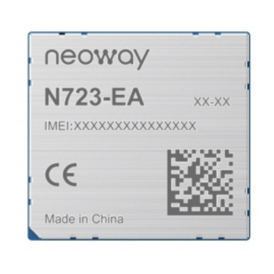
Page 68: Label
N723-EA Hardware User Guide Chapter 8 Mechanical Characteristics 8.2 Label The label information is laser carved on the cover. The following figure shows the label of N723-EA. Figure 8-2 N723-EA label The picture above is only for reference. 8.3 Packing N723-EA adopts the SMT method for oven soldering. -
Page 69: Moisture
The picture above is only for reference. 8.3.2 Moisture N723-EA is a level 3 moisture-sensitive electronic element, in compliance with IPC/JEDEC J-STD-020 standard. After the module is unpacked, if it is exposed to the air for a long time, the module will get damp, and may be damaged during reflow soldering or laboratory soldering. -
Page 70: Mounting
N723-EA Hardware User Guide Chapter 9 Mounting 9 Mounting This chapter describes the module PCB package and application PCB package of N723-EA, as well as the key points of SMT related technology. 9.1 PCB Package Figure 9-1 N723-EA bottom view of PCB package (unit: mm) -
Page 71: Application Foot Print
Chapter 9 Mounting 9.2 Application Foot Print The N723-EA module has a total of 100 pins in LGA package, and the recommended application PCB package is as follows: Only GND via-holes and pour coppers are allowed in the shaded area " ” of the PCB package to ensure the proper operation of the module. -
Page 72: Solder Paste
220 °C for more than 45 seconds and the peak temperature reaches 240 °C. 9.5 SMT Oven Temperature Profile Neoway will not provide warranty for heat-responsive element abnormalities caused by improper temperature control. Thin or long PCB might bend during SMT. So, use loading tools during the SMT and reflow soldering process to avoid poor solder joint caused by PCB bending. - Page 73 245 °C (depending on the type of the solder paste), and heat the module till the solder paste is melted. Then remove the module using tweezers. Do not shake the module at high temperatures while removing it. Otherwise, the components inside the module might get misplaced. Copyright © Neoway Technology Co., Ltd. All rights reserved.
-
Page 74: Abbreviation
Global Navigation Satellite System GPIO General Purpose Input Output 3GPP 3rd Generation Partnership Project GPRS General Packet Radio Service Global System for Mobile Communications Inter-Integrated Circuit Input/Output Leadless Chip Carriers Light Emitting Diode Copyright © Neoway Technology Co., Ltd. All rights reserved. - Page 75 Time Division Duplex UART Universal Asynchronous Receiver-Transmitter Uplink Universal Serial Bus USIM Universal Subscriber Identity Module VBAT Battery Voltage WiFi Wireless Fidelity WCDMA Wide-band Code Division Multiple Access WLAN Wireless Local Area Network Copyright © Neoway Technology Co., Ltd. All rights reserved.
Need help?
Do you have a question about the N723-EA and is the answer not in the manual?
Questions and answers