Table of Contents

Related Manuals for Sony CDP-CX240


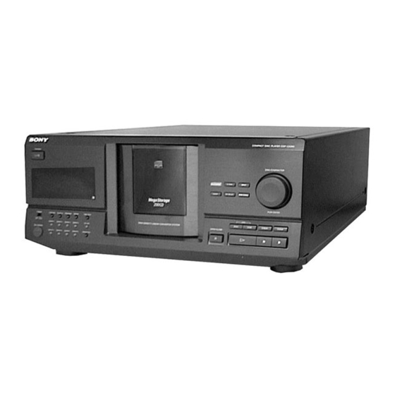
Summary of Contents for Sony CDP-CX240
- Page 1 CDP-CX240 SERVICE MANUAL US Model Canadian Model Model Name Using Similar Mechanism CDP-CX250 CD Mechanism Type CDM-40B Base Unit Type KSM-213BKN/M-N Optical Pick-up Type KSS-213B/S-N SPECIFICATIONS COMPACT DISC PLAYER MICROFILM – 1 –...
- Page 2 LES DIAGRAMMES SCHÉMATIQUES ET LA LISTE DES PIÈCES SONT CRITIQUES POUR LA SÉCURITÉ DE FONCTIONNEMENT. NE REMPLACER CES COMPOSANTS QUE PAR DES PIÈCES SONY DONT LES NUMÉROS SONT DONNÉS DANS CE MANUEL OU DANS LES SUPPLÉMENTS PUBLIÉS PAR SONY. – 2 –...
-
Page 3: Table Of Contents
SECTION 1 SERVICING NOTE TABLE OF CONTENTS NOTES ON HANDLING THE OPTICAL PICK-UP BLOCK OR BASE UNIT 1. SERVICING NOTE ............3 The laser diode in the optical pick-up block may suffer electrostatic 2. GENERAL ................6 break-down because of the potential difference generated by the charged electrostatic load, etc. - Page 4 CD-TEXT TEST DISC This unit is able to display the TEXT data (character information) written in the CD on its fluorescent indicator tube. The CD-TEXT TEST DISC (TGCS-313:J-2501-126-A) is used for checking the display. To check, perform the following procedure. Checking Method: 1.
- Page 5 Table 2: CD-TEXT TEST DISC Recorded Contents and Display (In this unit, some special characters cannot be displayed. This is no a fault.) TRACK Recorded contents Display ! ” # $ % & ´ (21h to 27h)1kHz 0dB L&R N All the same N All the same + , –...
-
Page 6: General
SECTION 2 GENERAL Front Panel 9 10 11 12 13 LOCATION OF PARTS AND CONTROLS 1 1/u (power) button 2 STANDBY indicator 3 Display window 4 Front cover 5 MEGA control button and indicator 6 X-FADE button 7 INPUT button 8 DISC/CHARACTOR dial and PUSH ENTER button 9 FADER button 10 NO DELAY button... -
Page 7: Disassembly
SECTION 3 DISASSEMBLY Note : Follow the disassembly procedure in the numerical order given. 3-1. FRONT PANEL ASSEMBLY 6 Remove the claw 1 Two screws (BVTP3x8) 2 Two screws (BVTP 3x8) 7 Front panel assembly 5 Remove the claw 4 Flat type wire (17 core) (Main board, CN501) 3 Four screws (BVTT3x6) -
Page 8: Base (Door, Gear) Assembly
3-3. BASE (DOOR, GEAR) ASSEMBLY 2 Three screws (BVTT3x6) MAIN board 4 Connector (CN503) 5 Guide assembly 3 Screw (PSW3x6) 1 Screw (BVTT3x6) 6 Door (CD) assembly 8 Three screws (BVTT3x6) 9 Base (Door, Gear) assembly 7 Three screws (BVTT3x6) 3-4. -
Page 9: Mechanism Deck
3-5. MECHANISM DECK 1 Flat type wire 5 Mechanism deck (23core) (CN502) Main board Jack board Main board 2 Connector (CN904) 3 Connector (CN505) 4 Nine screws (BVTT3x8) 3-6. BASE UNIT 1 Screw (BVTT3x6) 2 Fulcrum plate (BU Upper) assembly 3 Base unit –... -
Page 10: Test Mode
SECTION 4 TEST MODE 4-1. DISPLAY CHECK MODE 4-3. KEY AND DISPLAY CHECK MODE With the power turned off (standby state), press the 1/u button To set this mode, connect the test point (AFADJ) on the MAIN while pressing the P (pause) button. board to Ground, and connect the power supply plug to the outlet. - Page 11 4-4. AGING MODE Special Aging Mode Functions The aging mode is provided with the following convenient functions • Disc setting mode (*1) Aging Mode • Selection of presence of protection function during error (*2) • Mode which repeatedly changes and plays back discs automati- •...
- Page 12 Aging Method 1. Turn ON the power of the unit. Press the § OPEN/CLOSE and 7. Press the ( button. 8. The ( LED blinks, the aging mode is set, and aging is started. open the front cover. 2. Change the COMMAND MODE switch (S901) on set to CD1 . 9.
-
Page 13: Adjustments
SECTION 5 ADJUSTMENTS 5-1. MECHANICAL ADJUSTMENT Perform the following steps before carrying out adjustments. 1. Turn ON the power of the unit, set disc to disc table No. 92, and perform chucking. 2. Turn OFF the power. 3. Remove the case. 4. - Page 14 GUIDE (DISC T) ALIGNMENT Holder (guide T) Fixed screw Guide (disc T) (1) Rotate the cam and adjust to the position shown in the figure. (2) Check that the state is as Guide (disc T) shown in the figure. Disc Tapering screwdriver Guide (disc T) Disc...
- Page 15 HOLDER (DISC A) ALIGNMENT Holder (disc A) Thrust screw (1) Rotate the cam and adjust to the position shown in the figure. Disc 0 - 1mm Holder (disc A) (2) Check that the state is as shown in the figure. Disc Holder (disc A) Thrust screw...
- Page 16 SENSOR ALIGNMENT CAUTION: Perform this adjustment after the “holder (disc A) adjustment”. The LED may not light up in steps (3) and (4) for some If the disc table swings to the left and right just before the disc is microprocessor versions, and consequently adjustments will not chucked, perform the following adjustment.
- Page 17 PULLY AND DISC CENTER HOLE ALIGNMENT Base unit Bracket (BU adjustment) (1) Rotate the cam and adjust to the position shown in the figure. Magnet assembly (2) Check that the state is as shown in the figure. 0.5 - 2mm Disc Disc pulley Disc hole...
- Page 18 MAGNET ASSY ALIGNMENT Adjustment screw Magnet assembly (1) Rotate the cam and adjust to the position shown in the figure. Disc Magnet holder Magnet assembly Adjustment screw (3) Apply suitable locking compaund to the part after adjusting. Adjustment screw (2) Rotate the adjustment screw until A=B or between A:B=2:1 and 1:2 –...
-
Page 19: Electrical Block Checking
5-2. ELECTRICAL BLOCK CHECKING Note: A clear RF signal waveform means that the shape “◊” can be clearly distinguished at the center of the waveform. Note: RF signal waveform 1. CD Block is basically designed to operate without adjustment. Therefore, check each item in order given. VOLT/DIV : 200mV TIME/DIV : 500ns 2. - Page 20 Disc Sensor Adjustment Procedure: 1. Connect the oscilloscope to Pins 1, 2, and 4 of CN506 of the Perform this adjustment after completing all adjustments of the MAIN board. Also connect a 1 kΩ resistor to Pin 4 at the same mechanism section.
- Page 21 14. After the adjustment, load a disc only in slit 1, and press the 1/ u button to turn off the power. 15. Press the 1/u button while pressing the PUSH ENTER button to turn on the power. 16. If the rotary table makes one round, and “YES” is displayed on the fluorescent indicator tube after it stops, it means that the adjustment has been performed properly.
-
Page 22: Diagrams
SECTION 6 DIAGRAMS 6-1. CIRCUIT BOARDS LOCATION D.SENS (LUMINOUS) board ILLUMINATION board T.SENS board MAIN board DISP board JACK board KEY BOARD board T.MOTOR board JOG board D.SENS (RAY-CATCHER) board DOOR SW board DOOR MOTOR board BD board L.SW board L.MOTOR board –... -
Page 23: Block Diagrams
CDP-CX240 6-2. BLOCK DIAGRAMS IC101 – BD SECTION – DIGITAL SIGNAL PROCESSOR OPTICAL PICK-UP IC103 BLOCK (KSS-213B) RF AMP LASER DIODE POWER IC901 APC LD DIGITAL DOUT DIGITAL OPTICAL DRIVE ASYO Q101 DETECTOR RFAC RF EQ SUMMING ASYI ASYMMETRY DIGITAL... -
Page 24: Main Section
CDP-CX240 – MAIN SECTION – D505 T901 J903 –30V REG –B POWER Q501 RECT TRANSFORMER MUTE 2ND CD IN Q324 D507 IC401 L901 IC302(1/2) IC302(2/2) MIX AMP LINE FL701 AC IN LOUT MUTE FILTER Q321 LINE OUT D503, 504 MUTE –VCC... - Page 25 WAVEFORMS THIS NOTE IS COMMON FOR PRINTED WIRING BOARDS AND SCHEMATIC DIAGRAMS. (In addition to this, the necessary note is printed in each block.) 3.1Vp-p For schematic diagrams. 16.9MHz Note: IC101 ^§ XTAI • All capacitors are in µF unless otherwise noted. pF: µµF 50 WV or less are not indicated except for electrolytics and tantalums.
-
Page 26: Schematic Diagram - Bd Section
CDP-CX240 6-3. SCHEMATIC DIAGRAM – BD SECTION – • See page 28 for Waveforms. • See page 47 for IC Block Diagrams. • See page 50 for IC Pin Functions. (Page 36) – 29 – – 30 –... -
Page 27: Printed Wiring Board - Bd Section
CDP-CX240 6-4. PRINTED WIRING BOARD – BD SECTION – • See page 22 for Circuit Boards Location. (Page 34) – 31 – – 32 –... -
Page 28: Printed Wiring Board - Main Section
CDP-CX240 6-5. PRINTED WIRING BOARD – MAIN SECTION – • See page 22 for Circuit Boards Location. • Semiconductor (Page 44) (Page 46) (Page 46) Location Ref. No. Location D325 D327 D329 D425 D501 D502 D503 D504 D505 D506 D507... -
Page 29: Schematic Diagram - Main (1/2) Section
CDP-CX240 6-6. SCHEMATIC DIAGRAM – MAIN (1/2) SECTION – • See page 28 for Waveforms. • See page 49 for IC Block Diagrams. • See page 52 for IC Pin Functions. (Page 29) (Page 45) (Page 45) (Page 45) (Page 45) -
Page 30: Schematic Diagram - Jack Section
CDP-CX240 6-7. SCHEMATIC DIAGRAM – JACK SECTION – • See page 22 for Waveforms. • See page 33 for Printed Wiring Board (MAIN BOARD). • See page 49 for IC Block Diagrams. – 38 – – 37 –... -
Page 31: Printed Wiring Board - Jack Section
CDP-CX240 6-8. PRINTED WIRING BOARD – JACK SECTION – • See page 22 for Circuit Boards Location. (Page 33) (Page 34) T901 POWER TRANSFORMER JW903 – 39 – – 40 –... -
Page 32: Schematic Diagram - Display Section
CDP-CX240 6-9. SCHEMATIC DIAGRAM – DISPLAY SECTION – • See page 49 for IC Block Diagrams. (Page 35) – 42 – – 41 –... -
Page 33: Printed Wiring Board - Display Section
CDP-CX240 6-10. PRINTED WIRING BOARD – DISPLAY SECTION – • See page 22 for Circuit Boards Location. (Page 33) • Semiconductor Location Ref. No. Location D701 D702 D703 D704 D705 D706 D707 D708 D709 D710 IC601 IC701 IC702 Q701 – 43 –... -
Page 34: Schematic Diagram - Sensor/Motor Section
CDP-CX240 6-12. PRINTED WIRING BOARD – SENSOR/MOTOR SECTION – 6-11. SCHEMATIC DIAGRAM – SENSOR/MOTOR SECTION – • See page 22 for Circuit Boards Location. (Page 33) (Page 35) (Page 35) (Page 34) (Page 33) (Page 33) (Page 35) (Page 34) -
Page 35: Ic Block Diagrams
6-13. IC BLOCK DIAGRAMS • BD section IC101 CXD2587Q ERROR DIGITAL CORRECTOR ASYMMETRY DIGITAL CORRECTION OPERATIONAL LRCK AMPLIFIER ANALOG SWITCH PCMD INTERFACE DEMODULATOR CONVERTER EMPH XVDD XTAI TIMING LOGIC CLOCK XTAO XTSL GENERATOR XVSS TES1 AVDD1 TEST AOUT1 SERVO DSP PWM GENERATOR AIN1 FRDR... - Page 36 IC102 BA6392FP BUFF CH1 OUT F 28 GND BUFF BUFF CH1 OUT R 27 CH4 OUT F LEVEL SHIFT CAPA IN 1 26 CH4 OUT R BUFF CH1 R IN 25 VB IN INTERFACE CH1 F IN 24 VS IN BUFF VREF IN 23 VB IN...
- Page 37 • Main (1/2) section • Main (2/2) section IC503 CXA1291P IC506 LA5616 VIN1 ON/OFF AMP1 CURRENT AMP2 LIMITER OVERHEAT ON/OFF PROTECT THERMAL SHUT VREF DOWN AND CURRENT LIMITER AMP3 RESET GENERATOR ERROR ERROR VIN2 • Display section IC702 M66310FP – 49 –...
-
Page 38: Ic Pin Functions
6-14. IC PIN FUNCTIONS • IC101 DIGITAL SIGNAL PROCESSOR (CXD2587Q) Pin No. Pin Name Function SQSO Sub-Q 80-bit and PCM peak level data output (CD text data output) SQCK Clock input for SQSO read-out XRST System reset “L” : reset SYSM Muting input “H”... - Page 39 Pin No. Pin Name Function Tracking error signal input Center servo analog input RFDC RF signal input Test pin (Not used) ADIO – Analog ground AVSS0 IGEN Stabilized current input for operational amplifiers – AVDD0 Analog power supply EFM full swing output ASYO ASYI Asymmetry comparate voltage input...
- Page 40 • IC501 SYSTEM CONTROL (CXP84340-094Q) Pin No. Pin Name Function SRAM address SRAM address SRAM address SRAM address SRAM address SRAM address SRAM address SRAM address SRAM address SRAM address SRAM address SRAM address SRAM writing SRAM enable KBCOUT Keyboard clock output KBDOUT Keyboard data output KBDIN...
- Page 41 Pin No. Pin Name Function Model select switch input KEY3 Key input KEY2 Key input KEY1 Key input KEY0 Key input BUSIN CONTROL-A1 input L: Active AMUTE Audio mute driver Clock for servo IC and digital filter IC Latch for command DATA Data for command Clock for sub code Q...
-
Page 42: Exploded Views
SECTION 7 EXPLODED VIEWS NOTE: The components identified by • Hardware (# mark) list and accessories and packing • Items marked “*” are not stocked since they are mark ! or dotted line with mark materials are given in the last of this parts list. seldom required for routine service. -
Page 43: Disc Table Section
7-2. DISC TABLE SECTION not supplied supplied not supplied not supplied not supplied supplied supplied not supplied M801 not supplied supplied M810 Ref. No. Part No. Description Remark Ref. No. Part No. Description Remark * 51 1-661-466-11 T.MOTOR BOARD * 73 4-982-802-01 RING (A) X-4947-230-1 BRACKET (TABLE) ASSY * 74... -
Page 44: Front Panel Section
4-998-523-01 KNOB (JOG) * 109 4-982-811-01 HOLDER (FL) X-4949-663-1 PANEL ASSY, FRONT * 110 A-4724-061-A DISP BOARD, COMPLETE 1-783-365-11 WIRE (FLAT TYPE) (17 CORE) 4-996-698-01 EMBLEM, SONY 3-917-216-21 KNOB (TIMER) 4-985-553-21 CUSHION 4-977-358-11 CUSHION 4-996-682-11 INDICATOR * 106 1-669-165-11 KEY BOARD BOARD 4-996-683-21 BUTTON (POWER) 4-951-620-01 SCREW (2.6X8), +BVTP... -
Page 45: Mechanism Section-1 (Cdm-40B)
7-4. MECHANISM SECTION-1 (CDM-40B) not supplied not supplied not supplied not supplied Ref. No. Part No. Description Remark Ref. No. Part No. Description Remark X-4947-241-1 LEVER (C) ASSY A-4672-092-A MAGNET ASSY 4-982-882-01 SPRING (LIMITTER), TORSION 3-366-559-02 MAGNET (CHUCK) 4-982-881-01 SPRING (HOLDER), TORSION 4-960-633-01 YOKE (MAGNET) X-4947-239-1 LIMITTER (A) ASSY 4-982-853-01 LEVER (B) -
Page 46: Mechanism Section-2 (Cdm-40B)
7-5. MECHANISM SECTION-2 (CDM-40B) not supplied not supplied not supplied M802 Ref. No. Part No. Description Remark Ref. No. Part No. Description Remark 4-976-465-01 GEAR (LOADING 1) X-4947-227-1 LEVER (STOPPER) ASSY 4-976-466-01 GEAR (LOADING 2) 4-982-893-01 GEAR (CENTER 2) 4-951-291-01 SCREW X-4947-607-1 GEAR (PULLEY) ASSY X-4947-234-1 SLIDER (LOCK) ASSY 4-982-867-01 BELT (TIMING) -
Page 47: Mechanism Section-3 (Cdm-40B)
7-6. MECHANISM SECTION-3 (CDM-40B) Ref. No. Part No. Description Remark Ref. No. Part No. Description Remark 3-356-601-11 SCREW, STEP 4-982-872-01 SPRING (F-2), TENSION X-4947-244-1 SLIDER (BU ADJUSTMENT) ASSY 4-982-871-01 SPRING (F-1), TENSION X-4947-243-1 HOLDER (BU) ASSY 4-982-858-01 DAMPER 4-982-859-01 HOLDER (DAMPER) 4-960-617-01 CAP (F) 4-982-878-01 SPRING (F), COMPRESSION –... -
Page 48: Base Unit Section (Ksm-213Bkn/M-N)
7-7. BASE UNIT SECTION (KSM-213BKN/M-N) not supplied not supplied not supplied M101 not supplied M102 Les composants identifiés par une The components identified by marque ! sont critiques pour la mark ! or dotted line with mark ! are critical for safety. sécurité. -
Page 49: Electrical Parts List
SECTION 8 ELECTRICAL PARTS LIST Note: • Due to standardization, replacements in the parts list • SEMICONDUCTORS The components identified by In each case, u: µ , for example: may be different from the parts specified in the mark ! or dotted line with mark uA...: µ... - Page 50 D.SENS (LUMINOUS) D.SENS (RAY CATCHER) DISP Ref. No. Part No. Description Remark Ref. No. Part No. Description Remark R138 1-216-295-91 SHORT C707 1-162-282-31 CERAMIC 100PF R143 1-216-103-00 METAL CHIP 180K 1/10W C708 1-162-282-31 CERAMIC 100PF R144 1-216-103-00 METAL CHIP 180K 1/10W C709 1-162-288-31 CERAMIC...
- Page 51 DISP DOOR MOTOR DOOR SW ILLUMINATION JACK Ref. No. Part No. Description Remark Ref. No. Part No. Description Remark R733 1-249-417-11 CARBON 1/4W F < DIODE > R734 1-249-419-11 CARBON 1.5K 1/4W F R735 1-249-421-11 CARBON 2.2K 1/4W F D802 8-719-059-65 DIODE HLMF-KL05 D803 8-719-059-65 DIODE HLMF-KL05...
- Page 52 JACK L.MOTOR L.SW MAIN Ref. No. Part No. Ref. No. Description Part No. Description Remark Remark R902 1-249-425-11 CARBON 4.7K 1/4W F S626 1-572-184-11 SWITCH, KEYBOARD (FADER) R903 1-249-429-11 CARBON 1/4W S627 1-572-184-11 SWITCH, KEYBOARD (MEGA CONTROL) R921 1-249-429-11 CARBON 1/4W ************************************************************** <...
- Page 53 MAIN Ref. No. Part No. Description Remark Ref. No. Part No. Description Remark C405 1-126-022-11 ELECT 47uF D509 8-719-911-19 DIODE 1SS119-25 C501 1-128-489-11 ELECT 3300uF D521 8-719-911-19 DIODE 1SS119-25 C502 1-124-360-00 ELECT 1000uF < IC > C503 1-124-122-11 ELECT 100uF C504 1-126-021-11 ELECT 33uF...
- Page 54 MAIN T.MOTOR T.SENS Ref. No. Part No. Description Remark Ref. No. Part No. Description Remark R321 1-249-421-11 CARBON 2.2K 1/4W F R544 1-249-429-11 CARBON 1/4W R322 1-249-421-11 CARBON 2.2K 1/4W F R323 1-249-421-11 CARBON 2.2K 1/4W F R551 1-247-887-00 CARBON 220K 1/4W R552...
- Page 55 T.SENS Ref. No. Part No. Description Remark Ref. No. Part No. Description Remark IC803 8-749-924-18 IC PHOTO INTERRUPTER RPI-1391 ************** (TABLE SENSOR) HARDWARE LIST ************** < RESISTOR > 7-685-646-79 SCREW +BVTP 3X8 TYPE2 N-S R801 1-249-416-11 CARBON 1/4W F 7-685-871-01 SCREW +BVTT 3X6 (S) R802 1-249-416-11 CARBON 1/4W F...
- Page 56 CDP-CX240 98F097024-1D Sony Corporation Printed in Singapore © 1998. 6 9-922-884-11 Home A&V Products Company Published by Quality Assurance Dept. – 68 – (Shibaura)