Table of Contents
Advertisement
ORDER No. AD0009166C3
Portable Video CD Player
SL-VP48 / SL-VP43 / SL-VP33
Traverse Deck: RAE0145Z Mechanism Series
Colours
(S)............Silver Type
(N)............Gold Type
Areas
GK..............China.
GH..............Hong Kong.
GCS...........Asia, Latin America, Middle Near East, Africa and Oceania.
SPECIFICATIONS
1
Advertisement
Table of Contents

Related Manuals for Panasonic SL-VP48


Summary of Contents for Panasonic SL-VP48
- Page 1 ORDER No. AD0009166C3 Portable Video CD Player SL-VP48 / SL-VP43 / SL-VP33 Traverse Deck: RAE0145Z Mechanism Series Colours (S)....Silver Type (N)....Gold Type Areas GK....China. GH....Hong Kong. GCS...Asia, Latin America, Middle Near East, Africa and Oceania. SPECIFICATIONS...
- Page 2 Output voltage: 1.0Vp-p(75 General Power supply: DC 4.5V Power consumption: SL-VP33 Using AC adaptor: 4.8W SL-VP48/SL-VP43 AC adaptotr; Audio CDs(Anti-shock OFF/ON): 4.8W/5.0W Video CDs: 4.8W When rechargeing: 5.6W Play time (When used in hold mode, at 25°C temperature and on flat and stable surface.)
- Page 3 2 Alkaline batteries; Audio CDs(Anti-shock OFF/ON): About 18/19 hours Video CDs: About 3 hours Rechargeable batteries(P-3GAVT); Audio CDs(Anti-shock OFF/ON): About 9/9.5 hours Video CDs: About 2 hours The play time may be less depending on the operating condetions. Recharging time: About 3 hours Dimensions(WxHxD): 128x29.3x135mm...
-
Page 4: Precaution Of Laser Diode
(RFEA413T-1W) For GCS area - AC adaptor..............1 pc. (RFEA413Z-W) For GH area - AC adaptor..............1 pc. (RFEA413H-W) 2. Precaution of Laser Diode Caution: This product utilizes a laser diode with the unit turned “on”, invisible laser rediation is emitted from the pickup lens. / Wave length: 780nm / Maximum output radiation power from pickup: 100 W/VDE / Laserradiation from the pickup lens is safety level, but be sure the followings: 1. -
Page 5: Handling Precautions For Traverse Deck
3. Handling Precautions for Traverse Deck The laser diode in the traverse deck (optical pickup) may break down due to potential difference caused by static electricity of clothes or human body. So, be careful of electrostatic breakdown during repair of the traverse deck (optical pickup). 3.1. - Page 6 3.2. Grounding for electrostatic breakdown prevention 1. Human body grounding Use the anti-static wrist strap to discharge the static electricity from your body. (as shown in Fig. 3 2. Work table grounding Put a conductive material (sheet) or steel sheet on the area where the traverse deck (optical pickup) is placed, and ground the sheet.
-
Page 7: Operation Checks And Component Replacement Procedures
4. Operating Instructions 5. Operation Checks and Component Replacement Procedures - This section describes procedures for checking the operation of the major printed circuit boards and replacing the main components. - For reassembly after operation checks or replacement, reverse the respective procedures. - Page 9 - Check the video P.C.B. (A side) as shown below. 5.1.2. Checking for the video P.C.B. / (B side)
-
Page 10: Checking For The Main P.c.b
5.2. Checking for the main P.C.B. 5.2.1. Checking for the main P.C.B. / (A side) - Follow the (Step 1) - (Step 7) of item 5.1.1. - Page 11 - Check the main P.C.B. (A side) as shown below. 5.2.2. Checking for the main P.C.B. / (B side) - Follow the (Step 1) - (Step 6) of item 5.1.1.
- Page 12 - Check the main P.C.B. (B side) as shown below. 5.3. Replacement for the CD cover ass’y, LCD and JOG knob - Follow the (Step 1) - (Step 5) of item 5.1.1.
-
Page 15: Replacement For The Traverse Motor
5.4. Replacement for the traverse motor - Follow the (Step 1) - (Step 5) of item 5.1.1. -
Page 16: Replacement For The Optical Pickup
5.5. Replacement for the optical pickup - Follow the (Step 1) - (Step 5) of item 5.1.1. - Page 17 - Follow the (Step 1) - (Step 5) of item 5.4.
-
Page 18: Display Of Self-Diagnostic Function
6. Display of Self-Diagnostic Function This unit (SL-VP33/VP43/VP48) has self-diagnostic function, it may display below-mentioned on the LCD of this unit. - The substance of self-diagnostic display. In the case of this display, it may be causing for abnormally movements of traverse deck, touching failure of REST det. - Page 19 Check the operations described below on the traverse deck after replacing it. *Checking Skip Search 1. Play an ordinary musical program disc. 2. Press the skip button to check for normal skip search operation (in both the forward and reverse directions). *Checking Manual Search 1.
-
Page 20: Automatic Adjustment Results Display Function (Self-Check Function)
occurs. 2. Play the middle tracks of the uneven test disc (SZZP1056C) and verify that no sound skip or noise occurs. 8. Automatic Adjustment Results Display Function (Self-check Function) On this unit (SL-VP33/VP43/VP48), each automatic adjustment results are displayed on the LCD. This function is convenient to check or identify which automatic adjustment circuit is incorrect. - Page 21 8.2. Display of automatic adjustment results (self-check function) <Example> Follow the below steps when “E-1” is displayed. (Cause: Focus balance (FBC) is set beyond the limit.) - Check if 1. the waveform or voltage of the focus servo circuit is correct. (check the waveform or voltage.) 2.
- Page 22 3. the optical pickup returns to the normal state by exchanging the traverse deck. Follow the below steps when “E-F” is displayed. (Cause: All adjustments (TGC, FGC, TBC, FBC) are set beyond the limit.) - Check if 1. the optical pickup returns to the normal state by exchanging the traverse deck.
-
Page 23: Measurements And Adjustments
10. Measurements and Adjustments Warning: This product uses a laser diode. Refer to caution statements. 10.1. Measuring instruments and special tools Test discs 1. Playability test disc (SZZP1054C) 2. Uneven test disc (SZZP1056C) 3. Musical program disc (ordinary) 4. DC voltmeter 5. -
Page 24: Adjustment Procedure
10.4. Adjustment procedure 10.4.1. Power supply voltage adjustment 1. Connect the DC voltmeter to MVcc and GND on the P.C.B. 2. Connect the AC adaptor cord to the DC (IN) port and move the PLAY switch to the ON position. Anti-shock is set in OFF position. (Use a new dry cell battery or a rechargeable battery that is full charged.) 3. -
Page 25: Troubleshooting Guide
1. Play an ordinary musical program disc. 2. Press the manual search button to check for smooth manual search operations at either low or high speed (in both the forward and backward directions). *Checking Playability 1. Play the 0.7mm black dot and the 0.7mm wedge on the playability test disc (SZZP1054C) and verify that no sound skip or noise occurs. - Page 26 11.3. Master clock system waveform 11.4. Audio data clock system waveform 11.5. Diagnostic Procedures by Symptom...
- Page 27 Symptom Likely Location Fault CD-DA Video-CD TOC NG TOC NG (both audio and For TOC NG, fault in the CD-DA circuit. video are NG.) Blue back IC501, IC11, or traverse system. display. Turntable fails to rotate. Fails to rotate. Traverse system, focus servo system ( IC11), supply line, clock line system control (IC301).
-
Page 30: Schematic Diagram Notes
12. Schematic Diagram Note 12.1. Type Illustration of IC's, Transistors and Diodes 12.2. Schematic Diagram Notes Notes:... - Page 31 : Laser ON/OFF switch in “OFF” position. / (It turns “ON” with disc holder closed.) S201 : Rest detector in “OFF” position. / (It turns “ON” when optical pickup comes to S202 innermost periphery.) Select/play/pause button ( , SELECT) S301 Stop/operation off button ( , STOP/OPR S302...
- Page 32 play mode, and the other, for no disc in stop mode. - AC adaptor is used for power supply. - Voltage and signal line : Positive Voltage Line : CD-DA/VCD (Audio) Signal Line : CD-DA/VCD (Audio & Video) Signal Line : VCD (Video) Signal Line : MIC Signal Line Impotant safety notice:...
- Page 33 Mark I/O / Function Division Tracking signal input (1) terminal Tracking signal input (2) terminal Power supply input terminal Focus signal input (1) terminal Focus signal input (2) terminal APC amplifier input terminal APC amplifier output terminal RF addition output terminal RF IN RF detection signal input terminal...
- Page 34 terminal Mark I/O / Function Division TBAL Tracking balance signal input terminal FBAL Focus balance signal input terminal 16.2. IC301(M38258M901GP): System Control / LCD Drive Mark I/O / Function Division 1~3 KEY1 / Key switch signal input ~KEY3 Mode (NORMAL, PBC, OFF, RESUME) input SEL2 Not used, connected to GND...
- Page 35 Mark I/O / Function Division /HOLD Hold signal input — GND terminal /RESET Reset signal input DEMPH DAC emphasis signal input — Not used, open SMCK Clock signal input — Not used, open — GND terminal — Not used, open VMUTE Video muting signal output MUTE...
- Page 36 Mark I/O / Function Division VREF Reference voltage input — GND terminal 92~95 COM3 / LCD common signal output ~COM0 Control voltage input Control voltage input — Not used, open 98~99 Control voltage input 16.3. IC401(AN8746SAE1): Coil and Motor Drive Mark I/O / Function...
- Page 37 Mark I/O / Function Division Traverse motor (+) drive signal input terminal Traverse motor (-) drive signal input terminal Traverse motor (-) drive signal output terminal PGND3 — GND terminal Traverse motot (+) drive signal output terminal Traverse motot (+) drive signal output terminal PGND4 —...
- Page 38 Mark I/O / Function Division Coil drive input terminal for VG voltage increase (connected to power supply) PGND2 — GND terminal IOUT Charging signal and charging feedback output terminal Power supply input terminal REGB Regulator drive signal output terminal 15 MSTAT/ DC jack detection output / ACDET terminal...
- Page 39 Mark I/O / Function Division Triangular wave output terminal / (connected GND through capacitor) SPRT Output terminal for setting of constants anti-power OFF / (connected to GND through capacitor) — DC/DC converter OFF(Not used, open) BOUT Amplifier output terminal (Not used, open) 35 STROBE Strobe input terminal Sub DC/DC converter error...
- Page 40 Mark I/O / Function Division — Power supply (digital circuit) terminal SPOUT Spindle motor drive output terminal TRV+ Traverse motor drive output terminal TRV- Traverse motor drive output terminal Tracking coil drive output terminal Tracking coil drive output terminal Focus coil drive output terminal Focus coil drive output terminal...
- Page 41 Mark I/O / Function Division PLLF PLL loop filter output terminal VCOF VCO loop filter output terminal — Power supply (analog circuit) terminal — GND (analog circuit) terminal OUTL Lch audio signal output terminal — GND (analog circuit) terminal OUTR Rch audio signal output terminal —...
-
Page 42: Replacement Parts List
Mark I/O / Function Division 67 DMUTE/ Muting signal output (“H” : Mute)/Serial data signal SRDATA output STAT Status signal output terminal NRST Reset signal input terminal (“L” : Reset) SPPOL Spindle motor drive signal output terminal PMCK Frequency division clock signal output (f=88.2Hz) SMCK System clock output (f=... - Page 43 *Capacity values are in microfarads ( F) unless specified otherwise, P=Pico-farads (pF), F= Farads (F). Resistance values are in ohms, unless specified otherwise, 1K=1,000 (OHM), 1M=1,000k (OHM). *The marking (RTL) indicates that the Retention Time is limited for this item. After the discontinuation of this assembly in production, the item will continue to be available for a specific period of time.
- Page 44 Ref. No. Part No. Part Name & Description Remarks RGU1838-H OPEN KNOB RKM0430A-H INTERMEDIATE CABINET (VP33/VP43) RKM0430-H INTERMEDIATE CABINET (VP48) RML0580 STOPPER RGN1967-K NAME PLATE (VP33GK) RGN1968-K NAME PLATE (VP33GCS) RGN1965-K NAME PLATE (VP43GK) RGN1966-K NAME PLATE (VP43GCS) RGN1962-K NAME PLATE (VP48GK) RGN1963-K NAME PLATE...
- Page 45 Ref. No. Part No. Part Name & Description Remarks C120 ECUV1H152KBV 50V 1500P F1H1H152A013 C121 ECUV1H121JCV 50V 120P C201 RCST0GY476RG 4V 47U F3F0G4760001 C301 ECUVNA224KBV 10V 0.22U F1H1A224A028 C351 ECST0JY475RR 6.3V 4.7U ECST0JY475R C352 ECUVNC104KBV 16V 0.1U C401 ECUZNC104ZFV 16V 0.1U F1H1C1040008 C402-05 ECUVNA105ZFV...
- Page 46 Ref. No. Part No. Part Name & Description Remarks C761,62 ECUVNA105ZFV 10V 1U F1H1A105A030 (VP48) C763 ECUVNH103KBV 50V 0.01U F1H1H103A748 (VP48) C764 ECUV1H102KBV 50V 1000P (VP48) C765 ECUVNC104KBV 16V 0.1U (VP48) C766,67 ECUVNA224KBV 10V 0.22U F1H1A224A028 (VP48) C768 RCST0GY476RG 4V 47U F3F0G4760001 (VP48) C769...
- Page 47 Ref. No. Part No. Part Name & Description Remarks MA111TX DIODE MA2J11100L D101 MA111TX DIODE MA2J11100L D301 M1MA141WKT1 DIODE B0ADBA000001 D851 MA111TX DIODE MA2J11100L D871 MA8051M DIODE MAZ80510M D872 MA111TX DIODE MA2J11100L D903 M1MA141WKT1 DIODE B0ADBA000001 IC11 RS10003E2 IC101 AN8839NSBE2 AN8839NSB-E2 IC301 M38258M901GP...
- Page 48 Ref. No. Part No. Part Name & Description Remarks RPK1477 PACKING CASE (VP43GCS) RPK1474 PACKING CASE (VP48GK) RPK1475 PACKING CASE (VP48GCS) RPK1525 PACKING CASE (VP48GH) RPQ0836-1 RPQ0869-1 RPQ1109 RPF0111 PROTECTION BAG(UNIT) PCB1 REP2518M-T MODULE P.C.B. (RTL) PCB2 REP3066C-M MAIN P.C.B. (RTL)(VP33) PCB2 REP3066B-M...
- Page 49 Ref. No. Part No. Part Name & Description Remarks R113,14 ERJ3GEYJ330V 1/16W 33 D0GB330JA002 R120 ERJ3GEYJ103Z 1/16W 10K R121,22 ERJ3GEYJ124V 1/16W 120K D0GB124JA002 R201 ERJ3GEYJ2R2V 1/16W 2.2 D0GB2R2JA002 R202 ERJ3GEYJ223V 1/16W 22K D0GB223JA002 R301 EXBV8V473JV 1/16W 47K R302 EXBV8V104JV 1/16W 100K R303-05 ERJ3GEYJ102V 1/16W 1K...
- Page 50 Ref. No. Part No. Part Name & Description Remarks R756 ERJ3GEYJ472V 1/16W 4.7K D0GB472JA002 (VP48) R757 ERJ3GEYJ103Z 1/16W 10K (VP48) R758 ERJ3GEYJ683V 1/16W 68K D0GB683JA002 (VP48) R759 ERJ3GEYJ102V 1/16W 1K ERJ3GEYJ102Z (VP48) R760 ERJ3GEYJ473V 1/16W 47K D0GB473JA002 (VP48) R763 ERJ3GEYJ103Z 1/16W 10K (VP48) R765...
-
Page 51: Cabinet Parts Location
Ref. No. Part No. Part Name & Description Remarks R1007 ERJ3GEYD562V 1/16W 5.6K R1008 ERJ3GEYJ103Z 1/16W 10K R1009 ERJ3GEYD912V 1/16W 9.1K R1010,11 ERJ3GEYJ103Z 1/16W 10K R1012 ERJ3GEYD332V 1/16W 3.3K D0HB332ZA002 R1013,14 ERJ3GEYD750V 1/16W 75 R1020 ERJ3GEY0R00V 1/16W 0 RJ301 ERJ3GEY0R00V 1/16W 0 (VP48) RJ351... - Page 52 19. Packaging...
- Page 53 Printed in Japan (H000900000) SW/HH...
- Page 54 AN8839NSB-E1 IC101 OPTICAL PICKUP SERVO AMP RF IN CS BRT SEMICONDUCTOR RFENV OFTR 3 TENV LASER DET. Vref. OFTR OFTR Q201 Vref. LASER BDO DET. POWER DRIVE /RFDET NRFDET DET. Vref. FE IN SUBTRA- FE OUT CTOR Vref. Vref. VCBA Vref.
- Page 55 DSLF2 DSLF2 OUTPUT D/A CONVERTER PORT VREF VREF TIMING GENERATOR (DIRECT PWM) /RESET NRST 10~19 2,3, X501 (16.9MHz) [For SL-VP43 only] [For SL-VP48 only] 5,8~11, 1,2, 8~11, 2,3, 13~17 22,23 14~19 22,23 MNV4400DT8TL MNV7400CT10T IC502 IC502 4M DRAM 16M DRAM...
- Page 56 112 113 114 2,16,39, 18,22,41, 66,70, 47,53,80, 49,55,82, 74,87 99,104, 102,118, 116, S201 (LASER ON/OFF) BLKCK C2BBGE000434 IC301 MUTE0 SYSTEM CONTROL / LCD DRIVE D301 /PLAY S301 ,SELECT) NOR- SUME S202 S310 (REST DET.) (HOLD) S309 (MODE) [For SL-VP48 only]...
- Page 57 BUFFER VR701 Q601,602 C0ABBB000105 (VOLUME) MUTING IC601 HEADPHONES MUTING Q761 HEADPHONES Q701,702 MUTING HEADPHONES NJU7082BVAE1 IC701 Q753 [For SL-VP48 only] KMUTE MUTING CONT. /MIC C0ABBB000081 AREF IC751 +B6 +B3 CR network D903 Q604,608 MUTE MUTING Q755 AMUTE CONT. D/A CONV.
- Page 58 NOTE : CD-DA/VCD(AUDIO&VIDEO) SIGNAL LINE : CD-DA/VCD(AUDIO) SIGNAL LINE RS10003E2 : VCD(VIDEO) SIGNAL LINE IC11 DC-DC CONVERTER : MIC SIGNAL LINE AREF MSTAT/ AREF AVcc ACDET MCLK/ CHARGE MCLK MLD/ RIPPLE VCNT SERIAL FILTER REGISTER MDATA/ 8 BIT MEMORY MDATA CHGCMP BOUT RECHARGEABLE...
-
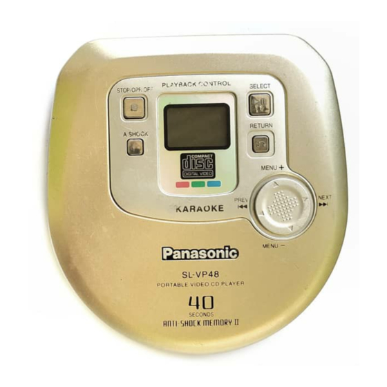
Page 59: Main Unit
Illustrations showing SL-VP48 are used in these in- structions Main unit Anti-shock button SL-VP48 SL-VP43 (A.SHOCK) 2 Stop/operation off button (∫, STOP/OPR OFF) 3 Display 4 Select/play/pause button (1;, SELECT) V I D 5 Return button (@, RETURN) A U D... - Page 60 TC7WU04FUT2L AN8746SA-E1 32PIN C0ABBB000105 8PIN M662782RPT1 80PIN AN8839NSB-E1 28PIN C0ABBB000081 14PIN MN89103M2 128PIN TC7W14FUTE1L LH5V2RN0 32PIN C1BB00000367 16PIN C2BBGE000434 100PIN NJU7082BVAE1 8PIN C0DBCAE00002 8PIN RS10003E2 40PIN No.1 No.1 MNV7400CT10T MNV4400DT8TL XP161A1265PR LC32V4260TLM B1BDND000001 B1GKCFEL0001 B1GFCFJA0006 MA2J70400L M1MA141WKT1 MA2J11100L FMW1T98 2SD1328TX Cathode Cathode XN0111500L...
- Page 61 SCHEMATIC DIAGRAM-1 SPINDLE TRAVERSE NOTE: S202 MOTOR MOTOR The number which noted at the connectors on the schematic diagram as (REST SWITCH) "SCHEMATIC DIAGRAM-1" or "SCHEMATIC DIAGRAM-2" indicates the schematic diagram serial number located MAIN CIRCUIT on the left corner in the schematic diagram. :POSITIVE VOLTAGE LINE CN401 :CD-DA/VCD(AUDIO &...
- Page 62 1 2 3 4 5 6 7 8 9 10 11 12 13 14 15 16 17 18 19 20 21 22 23 24 25 SL-VP48 ONLY R302 S314 100K RJ301 (NTSC/PAL) NTSC EXCEPT Z351 RCDRS-52 S309 SL-VP48 (REMOTE SENSOR) (MODE) R330 RESUME R352 For SL-VP48 ONLY R328 3.2V 3.2V 3.2V...
- Page 63 :CD-DA/VCD(AUDIO & VIDEO) SIGNAL LINE MAIN CIRCUIT :POSITIVE VOLTAGE LINE :CD-DA/VCD(AUDIO) SIGNAL LINE RJ516 3.2V For SL-VP43 ONLY For SL-VP48 ONLY IC502 IC502 MNV4400DT8TL MNV7400CT10T 4M DRAM 16M DRAM A B C D E F G H I J K L M N O P Q 0.8V...
- Page 64 SWITCHING B1GDCFJN0011 C805 RESET 2.9V 4V47 R804 3.2V 2.9V (0V) 3.2V 3.2V B1GBCFJJ0007 Q805 RESET B1GFCFJA0006 3.1V SWITCHING (0V) EXCEPT SL-VP48 (0.8V) RJ751 RJ351 R861 L851 C858 0.22 3.2V Q856 B1GKCFEL0001 POWER SUPPLY D903 2.8V 3.2V M1MA141WKT1 D851 C859 R855...
- Page 65 1.6V 1.6V 1.6V 1.6V 0.6V 0.4V 1.6V 1.6V 1.6V 3.2V 1.6V 1.6V 1.6V Q754,755 C764 1000P XN0111500L R775 SWITCHING R771 15K Q755 C762 1.6V 2.7V R770 1.6V C761 2.7V 1.6V R774 6.8K R788 Q762 1.6V RJ351 RJ751 2SD1328TX MUTING For SL-VP48 ONLY 5.2V 3.2V...
- Page 66 2 R6/LR6(UM-3) BATTERIES 2RECHARGEABLE BATTERYS 2.4V C802 0.01 Q608 B1GFCFJA0006 MUTING CONT. JK801 2.9V VIDEO OUT (PLUG TYPE:3.5mm) For SL-VP48 ONLY For SL-VP48 ONLY 2.9V For SL-VP48 ONLY RJ702 Q753 Q761 UN5511700L 2SD1328TX R752 C752 JK751 RJ703 25V0.47 MUTING CONT.
- Page 67 SCHEMATIC DIAGRAM-7 : POSITIVE VOLTAGE LINE : CD-DA/VCD (AUDIO) SIGNAL LINE VIDEO CIRCUIT : CD-DA/VCD (AUDIO & VIDEO) SIGNAL LINE : VCD(VIDEO) SIGNAL LINE 3.2V IC1003 TC7WU04FUT2L INVERTER (1.5V) 1.2V (1.5V) 1.3V (1.5V) 1.3V 2.6V F=27MHz 3.2V 1.5V R1000 5.6K X1000 (27MHz) 3.2V...
- Page 68 SCHEMATIC DIAGRAM-8 : POSITIVE VOLTAGE LINE : CD-DA/VCD (AUDIO) SIGNAL LINE : CD-DA/VCD (AUDIO & VIDEO) SIGNAL LINE : VCD(VIDEO) SIGNAL LINE 3.2V IC1004 TC7W14FUTE1L INVERTER 1.5V L K J I W X Y Z 1.5V 1.5V TP23 TP25 1.5V TP11 TP12 3.2V...
- Page 69 S310 C509 C301 D301 HOLD CN101 CN301 C201 SHORT LAND S314 A:SL-VP48 ONLY NTSC B:SL-VP43 ONLY REP3066A-M . . . SL-VP48 VREF C:EXCEPT SL-VP33 REP3066B-M . . . SL-VP43 NTSC/PAL D:EXCEPT SL-VP48 REP3066C-M . . . SL-VP33 OPERATION LCD UNIT...
- Page 70 CN11 2 R6/LR6(UM-3) BATTERIES . . . 3V JK701 2 RECHARGEABLE BATTERIES . . . 2.4V HEADPHONE C702 IC701 C615 C618 Q604 B E B SL-VP48 IC601 ONLY C617 Q871 Q608 B E B C872 JK751 JK601 Q601 AUDIO C602...
- Page 71 ELECTRICAL PARTS LOCATION Ref. No. Lo. No. Ref. No. Lo. No. Ref. No. Lo. No. Ref. No. Lo. No. Ref. No. Lo. No. MAIN P.C.B. (SIDE:A) IC501 RJ504 R384 R788 C607 IC502 RJ505 R501 R801 C608 IC751 RJ511 R503 C609 R806 IC752 RJ512...
- Page 72 VIDEO P.C.B.(SIDE : B) VIDEO P.C.B.(SIDE : A) L1002 R1005 C1013 C1015 9695 C1009 CN1001 C1012 IC1003 R1020 IC1000 TP27 R1000 R1001 IC1004 TP28 TP29 TP22 TP26 TP13 TP19 TP25 TP12 TP18 TP24 IC1002 IC1001 TP23 TP17 TP30 (GND) TP10 TP21 TP16 TP15...
Need help?
Do you have a question about the SL-VP48 and is the answer not in the manual?
Questions and answers