Xilinx Virtex-5 FPGA ML555 User Manual
Hide thumbs
Also See for Virtex-5 FPGA ML555:
- User manual (385 pages) ,
- User manual (88 pages) ,
- User manual (28 pages)

Related Manuals for Xilinx Virtex-5 FPGA ML555


Summary of Contents for Xilinx Virtex-5 FPGA ML555
- Page 1 Virtex-5 FPGA ML555 Development Kit for PCI and PCI Express Designs User Guide UG201 (v1.4) March 10, 2008...
- Page 2 Xilinx reserves the right to make changes, at any time, to the Design as deemed desirable in the sole discretion of Xilinx. Xilinx assumes no obligation to correct any errors contained herein or to advise you of any correction if such be made. Xilinx will not assume any liability for the accuracy or correctness of any engineering or technical support or assistance provided to you in connection with the Design.
- Page 3 “Platform Flash Image Generation and Programming,” page 101 to include process steps and screen shots from ISE 9.1i. Inserted two new figures (Figure 4-11, page 105 Figure 4-12, page 105). UG201 (v1.4) March 10, 2008 www.xilinx.com Virtex-5 FPGA ML555 Development Kit...
- Page 4 Board,” page 15. Updated Figure 3-1, page 21 to reflect “as built” 30 MHz LVCMOS oscillator. Added reference and link to Xilinx application notes XAPP1022 and XAPP1002 in “Edge Connector for PCI Express Operation,” page 23. Added footnote 6 Table 3-1, page 24 to identify FPGA connection of PCIE_PERST.
-
Page 5: Table Of Contents
Available Xilinx Accessories ........ - Page 6 Specifying the Xilinx PROM Device ........
-
Page 7: Preface: About This Guide
This user guide is a description of the Virtex™-5 FPGA ML555 Development Kit for PCI™ ® and PCI Express designs. Complete and up-to-date documentation of the Virtex-5 family of FPGAs is available on the Xilinx website at http://www.xilinx.com/virtex5. Guide Contents This manual contains the following chapters: •... - Page 8 XAPP865, Hardware Accelerator for RAID6 Parity Generation / Data Recovery Controller with ECC and MIG DDR2 Controller 10. UG086, Xilinx Memory Interface Generator (MIG) User Guide 11. XAPP870, Serial ATA Physical Link Initialization with the GTP Transceiver of Virtex-5 LXT FPGAs www.xilinx.com...
-
Page 9: Additional Support Resources
Express designs found in the Virtex-5 LXT and SXT devices. The Endpoint Block Plus core is a Xilinx CORE Generator™ IP core included in the latest IP Update on the Xilinx IP Center. Included with the Xilinx IP are a data sheet, a getting started guide, and a user guide. -
Page 10: Typographical Conventions
Configuration Guide for more information. Italic font The address (F) is asserted after Emphasis in text clock event 2. Underlined Text Indicates a link to a web page. http://www.xilinx.com/virtex5 www.xilinx.com Virtex-5 FPGA ML555 Development Kit UG201 (v1.4) March 10, 2008... -
Page 11: Online Document
Cross-reference link to a location Figure 5 in the Virtex-5 FPGA Red text in another document Data Sheet Go to http://www.xilinx.com Blue, underlined text Hyperlink to a website (URL) for the latest documentation. Virtex-5 FPGA ML555 Development Kit www.xilinx.com UG201 (v1.4) March 10, 2008... - Page 12 Preface: About This Guide www.xilinx.com Virtex-5 FPGA ML555 Development Kit UG201 (v1.4) March 10, 2008...
-
Page 13: Chapter 1: Introduction
Parallel Bus Development for PCI Operation This Virtex-5 FPGA based kit provides a development platform for designing and verifying PCI and PCI-X™ applications utilizing Xilinx LogiCORE™ intellectual property (IP) cores in a 3.3V signaling environment. The ML555 board is intended to plug-in to a 3.3V keyed system board. - Page 14 Chapter 1: Introduction The ML555 board is supported by Xilinx LogiCORE IP versions 4 and 6, respectively. Each core has a primary version number, shown in Table 1-1, followed by a revision or build number. More information about the current versions of these cores is available in the LogiCORE data sheets for the PCI and PCI-X section of the PCI/PCI-X product lounge (refer to http://www.xilinx.com/products/logicore/lounge/lounge.htm).
-
Page 15: Serial Bus Development
Xilinx Platform Cable USB programming cable • ISE™ evaluation software For assistance with any of these items, contact your local Xilinx distributor or visit the Xilinx online store at www.xilinx.com. The heart of the kit is the ML555 board. This manual provides comprehensive information on this board. -
Page 16: Available Xilinx Accessories
The ML555 board has one set of SMA connectors connected to one of the GTP transceiver ports of the XC5VLX50T FPGA. Xilinx sells a number of SMA conversion module boards that permit the conversion of the on-board SMA interface to other popular multi-gigabit serial connector interfaces. -
Page 17: Conversion Module, Sma To Hssdc2 (Hw-Afx-Sma-Hssdc2)
ML555 Board The SMA to RJ45 conversion module can be ordered from Xilinx as part number HW-AFX- SMA-RJ45. Contact your local sales office for pricing information. Additional information on the conversion module is available from the Xilinx website at: www.xilinx.com/xlnx/xebiz/designResources/ip_product_details.jsp?key=HW-AFX-SMA-RJ45... - Page 18 Chapter 1: Introduction www.xilinx.com Virtex-5 FPGA ML555 Development Kit UG201 (v1.4) March 10, 2008...
-
Page 19: Documentation And Reference Design Cd
Documentation and Reference Design CD The CD included in the Virtex-5 FPGA ML555 board kit contains the board design files, including schematics, PCB layout, and bill of materials. FPGA and CPLD design constraint files are included on the CD. This file provides a signal listing and physical FPGA pin locations (LOC) constraint to get started designing user applications with the Xilinx ISE software. - Page 20 Chapter 2: Getting Started www.xilinx.com Virtex-5 FPGA ML555 Development Kit UG201 (v1.4) March 10, 2008...
-
Page 21: Chapter 3: Hardware Description
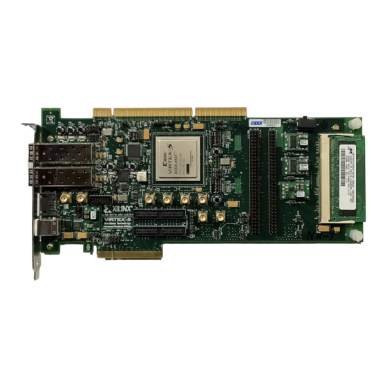
Chapter 3 Hardware Description A high-level block diagram of the Virtex-5 FPGA ML555 board is shown in Figure 3-1, followed by a brief description of each board section. Figure 3-2 is a photograph of the ML555 board with the key interfaces marked. - Page 22 J1: USB “B” User Pushbuttons/LEDS J3: SFP1 J4: SFP2 Serial ATA UG201_c3_02_022708 Figure 3-2: Annotated ML555 Board The CD included in the kit contains ML555 board schematics and layout files. www.xilinx.com Virtex-5 FPGA ML555 Development Kit UG201 (v1.4) March 10, 2008...
-
Page 23: Edge Connector For Pci Express Operation
PCI Express Designs P45: (Configure for PCI Express Lane Width Presence Detect) P18: (Install Shunts for PCI Express Designs) UG201_c3_03_022708 Figure 3-3: Connector and Power Management Headers for PCI Express Designs Virtex-5 FPGA ML555 Development Kit www.xilinx.com UG201 (v1.4) March 10, 2008... - Page 24 +3.3 VOLTS JTAG_TRST_B +3.3 VOLTS +3.3 VOLTSAUX PCIE_PERST PCIE_WAKE_B RESERVED PCIE_REFCLKP PCIE_REFCLKN PETP0 PETN0 PERP0 PERN0 PCIE_PRSNT2_B RESERVED PETP1 PETN1 PERP1 PERN1 PETP2 PETN2 PERP2 PERN2 PETP3 PETN3 PERP3 www.xilinx.com Virtex-5 FPGA ML555 Development Kit UG201 (v1.4) March 10, 2008...
- Page 25 6. PCIE_PERST connects to FPGA pin AE14. The PCI Express Card Electromechanical Specification requires add-in cards to implement variable-length edge finger pads and tie PRSNT1_B and PRSNT2_B signals together on the Virtex-5 FPGA ML555 Development Kit www.xilinx.com UG201 (v1.4) March 10, 2008...
- Page 26 ML555 development kit. Table 3-3 shows the correlation between PCI Express signals, P13 add-in card pin, FPGA pins, and GTP_DUAL tile location assignments. www.xilinx.com Virtex-5 FPGA ML555 Development Kit UG201 (v1.4) March 10, 2008...
- Page 27 PCIE_REFCLK_P PCIE_REFCLK_N PETP0 PETN0 PERP0 X0Y2 PERN0 PETP1 PETN1 PERP1 PERN1 PETP2 PETN2 PERP2 PERN2 X0Y1 PETP3 PETN3 PERP3 PERN3 PETP4 PETN4 PERP4 PERN4 X0Y3 PETP5 PETN5 PERP5 PERN5 Virtex-5 FPGA ML555 Development Kit www.xilinx.com UG201 (v1.4) March 10, 2008...
- Page 28 [Ref 6] for examples of how to get started designing and debugging PCI Express endpoint applications using the Integrated Endpoint Block for PCI Express designs available in Virtex-5 LXT FPGAs. www.xilinx.com Virtex-5 FPGA ML555 Development Kit UG201 (v1.4) March 10, 2008...
-
Page 29: 64-Bit Edge Connector For Pci Operation
P18: (Remove Shunts for PCI and PCI-X Modes) UG201_c3_04_092706 Notes: 1. SW8 and P18 must be configured for PCI power mode. Figure 3-4: PCI Connector and Power Management Headers Virtex-5 FPGA ML555 Development Kit www.xilinx.com UG201 (v1.4) March 10, 2008... - Page 30 In/Out EDGE_AD28 In/Out EDGE_AD26 In/Out EDGE_AD27 In/Out EDGE_AD25 In/Out EDGE_AD24 In/Out VCC3V3 EDGE_IDSEL EDGE_CBE3 In/Out VCC3V3 EDGE_AD23 In/Out EDGE_AD22 In/Out EDGE_AD20 In/Out EDGE_AD21 In/Out EDGE_AD19 In/Out EDGE_AD18 In/Out VCC3V3 www.xilinx.com Virtex-5 FPGA ML555 Development Kit UG201 (v1.4) March 10, 2008...
- Page 31 In/Out VCC3V3 EDGE_AD4 In/Out EDGE_AD5 In/Out EDGE_AD3 In/Out EDGE_AD2 In/Out EDGE_AD0 In/Out EDGE_AD1 In/Out VCC3V3 VCC3V3 EDGE_REQ64_B In/Out EDGE_ACK64_B In/Out VCC5 VCC5 VCC5 VCC5 64-Bit Connector unused EDGE_CBE7 In/Out Virtex-5 FPGA ML555 Development Kit www.xilinx.com UG201 (v1.4) March 10, 2008...
- Page 32 3. PCIBUSCLK1 is routed to FPGA global clock input pin J14, and PCIBUSCLK2 is routed to FPGA regional clock input pin L34. See “Clock Generation,” page 52 for information on how the PCI bus clock is connected on the ML555 board. www.xilinx.com Virtex-5 FPGA ML555 Development Kit UG201 (v1.4) March 10, 2008...
-
Page 33: Ml555 Configuration Headers For Pci Operation
PCI signal names. The ML555 board supports both PCI and PCI-X applications. The edge connector interfaces with the system board connector. Xilinx has LogiCORE solutions available for both PCI and PCI-X designs to facilitate getting started with the application-specific design. -
Page 34: Ddr2 Sdram Sodimm
The ML555 board contains a 200-pin, small-outline dual in-line memory module (SODIMM) connector (J2) that supports installation of DDR2 SDRAM SODIMMs of 128 MB, 256 MB, or 512 MB. Dual-rank SODIMMs are not supported. Xilinx provides a 256 MB DDR2-667 SODIMM Micron Semiconductor part number 4HTF3264HY-40E with the kit. - Page 35 DDR2 SDRAM SODIMM the DQ and DQS ports on the SODIMM side of the interface. The Xilinx Digitally Controlled Impedance (DCI) standard SSTL18_I_DCI can be utilized to terminate unidirectional address and control signals transmitted by the FPGA. External 50 Ω...
- Page 36 DDR2_VCC1V8 DDR2_VCC1V8 AH22 AG22 AG17 AH18 AF18 AE18 DDR2_VCC1V8 DDR2_VCC1V8 AG15 AH13 AH14 RAS_B AG13 WE_B AF19 S0_B AG18 DDR2_VCC1V8 DDR2_VCC1V8 CAS_B AH12 ODT0 AG30 No connect No connect www.xilinx.com Virtex-5 FPGA ML555 Development Kit UG201 (v1.4) March 10, 2008...
- Page 37 AG10 CK1_B AG11 DQS6_B AD11 In/Out DQS6 AD10 In/Out AP12 DQ50 AB10 In/Out DQ54 In/Out DQ51 AA10 In/Out DQ55 In/Out DQ56 In/Out DQ60 AC10 In/Out DQ57 In/Out DQ61 In/Out Virtex-5 FPGA ML555 Development Kit www.xilinx.com UG201 (v1.4) March 10, 2008...
- Page 38 DDR2 memory. This increases power dissipation rather than memory performance, and should be avoided for PCI Express and PCI bus applications where add-in card power is limited by specification to 25W. www.xilinx.com Virtex-5 FPGA ML555 Development Kit UG201 (v1.4) March 10, 2008...
-
Page 39: Small Form-Factor Pluggable (Sfp) Module Interface
8. Loss of signal from the SFP interface is connected to light emitting diode (LED) D7 for SFP1 and D8 for SFP2. The ML555 kit does not include SFP modules to plug into the connectors. The user must provide these. Virtex-5 FPGA ML555 Development Kit www.xilinx.com UG201 (v1.4) March 10, 2008... -
Page 40: Serial Ata Interface
SATA baud rates. A second SATA interface can be supported using the SMA connectors on the board and an external SMA to SATA interface board available from Xilinx with part number HW-AFX-SMA-SATA. The SATA and SMA transceivers are connected to a common GTP primitive block in the FPGA. -
Page 41: Sma Connectors
Another set of SMA connectors is also provided to input a clock to the GTP MGTREFCLK inputs. There are a number of Xilinx evaluation boards that convert an SMA interface to SATA, RJ45, or SFP, for example. - Page 42 , is 2.5V. See the ML555 board schematics on the CD-ROM for additional information. 3. These clocks are connected to FPGA clock-capable I/O pins. 4. NC = no connect. www.xilinx.com Virtex-5 FPGA ML555 Development Kit UG201 (v1.4) March 10, 2008...
- Page 43 CD-ROM for additional information. 2. NC = no connect. 3. These clocks are connected to FPGA clock-capable I/O pins. 4. These clocks are connected to FPGA global clock pins. Virtex-5 FPGA ML555 Development Kit www.xilinx.com UG201 (v1.4) March 10, 2008...
-
Page 44: Lvds Interface
16 LVDS data channels and a forwarded clock. A DDR SPI4.2 like interface consists of 16 LVDS data channels and one forwarded clock. Xilinx has several SDR and DDR LVDS reference designs that can be ported to run on the ML555 board. - Page 45 SAMTEC pin connections for P32 and P33, respectively. Table 3-12: SAMTEC Pin Connections (P32) SAMTEC-QSE- SAMTEC-QSE- FPGA FPGA 028-DP P32 Signal 028-DP P32 Signal Even GPIO1_I00_N GPIO1_I01_N GPIO1_I00_P GPIO1_I01_P No connect No connect Virtex-5 FPGA ML555 Development Kit www.xilinx.com UG201 (v1.4) March 10, 2008...
- Page 46 GPIO1_I09_P GPIO1_I10_N GPIO1_I11_N GPIO1_I10_P GPIO1_I11_P GPIO1_I12_N GPIO1_I13_N GPIO1_I12_P GPIO1_I13_P GPIO1_I14_N GPIO1_I15_N GPIO1_I14_P GPIO1_I15_P GPIO1_I16_N GPIO1_I17_N GPIO1_I16_P GPIO1_I17_P GPIO1_I18_N GPIO1_I19_N GPIO1_I18_P GPIO1_I19_P GPIO1_I20_N GPIO1_I21_N GPIO1_I20_P GPIO1_I21_P No connect No connect www.xilinx.com Virtex-5 FPGA ML555 Development Kit UG201 (v1.4) March 10, 2008...
- Page 47 AG12 GP1O2_I22_N AE12 No Connect No Connect No Connect No Connect GP1O2_I21_P GP1O2_I20_P GP1O2_I21_N GP1O2_I20_N GP1O2_I19_P GP1O2_I18_P GP1O2_I19_N GP1O2_I18_N GP1O2_I17_P GP1O2_I16_P GP1O2_I17_N GP1O2_I16_N GP1O2_I15_P GP1O2_I14_P GP1O2_I15_N GP1O2_I14_N GP1O2_I13_P GP1O2_I12_P Virtex-5 FPGA ML555 Development Kit www.xilinx.com UG201 (v1.4) March 10, 2008...
- Page 48 2.5V. See ML555 board schematics on the CD-ROM for additional information. 2. Bank 2 GPIO clock-capable I/O signals. All others are in FPGA Bank 18. 3. NC = no connect. 4. Bank 18 clock-capable I/O pins. www.xilinx.com Virtex-5 FPGA ML555 Development Kit UG201 (v1.4) March 10, 2008...
- Page 49 2. GPIO channel 1 of P32 connects to GPIO channel 1 of P33 when LVDS interface cable connects P32 to P33. 3. NC = No connection. Figure 3-6: LVDS Transmit and Receive Connections Between P32 and P33 Virtex-5 FPGA ML555 Development Kit www.xilinx.com UG201 (v1.4) March 10, 2008...
-
Page 50: Samtec Mezzanine Expansion Card Support
FPGA is at LVCMOS_25 standard levels. The user must provide a UART core internal to the FPGA to enable serial communication between the FPGA and USB attached serial port. UART cores are available from the Xilinx IP center at www.xilinx.com/ipcenter. Table 3-16 describes the RS-232 interface pin assignments. -
Page 51: Usb To Uart Bridge
PC prior to attempting to establish communications with the ML555 board. The device driver is on the ML555 CD-ROM. The driver allows the PC USB port to Virtex-5 FPGA ML555 Development Kit www.xilinx.com UG201 (v1.4) March 10, 2008... -
Page 52: Clock Generation
Consult the Virtex-5 FPGA User Guide for additional information on clocking and the appropriate I/O standards for high-speed clock and data signals. www.xilinx.com Virtex-5 FPGA ML555 Development Kit UG201 (v1.4) March 10, 2008... - Page 53 Input PCIE_REFCLKP Differential LVDS 100 MHz FPGA U10 GTP_DUAL tile X0Y2 MGTREFCLK_P (system board Spread pin Y4 and FPGA U10 global clock input pin J16 as input) Spectrum PCIE_GCLK_P Virtex-5 FPGA ML555 Development Kit www.xilinx.com UG201 (v1.4) March 10, 2008...
- Page 54 GTP_DUAL tiles for PCI Express operation. The architecture of the FPGA permits an external MGTREFCLK to be driven a maximum of three GTP_DUAL tiles up or down. See “Serial Bus Clocking with Optional ICS874003-02 Clock Jitter Attenuator (PCI Express Operation),” page 60 for additional information. www.xilinx.com Virtex-5 FPGA ML555 Development Kit UG201 (v1.4) March 10, 2008...
- Page 55 GTP X0Y5 SATA_MGT_REFCLKN MGT_REFCLKN 4.7KΩ Select SATA_MGT_CLKSEL Bank 3 I/O 200 MHz LVPECL_200M_P GCLKP LVPECL_200M_N LVPECL GCLKN PCICLK P1-B16 GCLK UG201_c3_18_022608 Figure 3-8: Clock Synthesis Block Diagram (Default Configuration) Virtex-5 FPGA ML555 Development Kit www.xilinx.com UG201 (v1.4) March 10, 2008...
- Page 56 Chapter 3: Hardware Description Figure 3-9 shows an optional clock synthesis configuration, which uses an ICS874003 jitter attenuator circuit. Contact your local Xilinx representative for more information on this option. U10 FPGA FPGA_GCLK_30MHZ GCLK SMA_GCLKP GCLKP SMA_GCLKN GCLKN PCIE250M_P MGT_REFCLKP...
-
Page 57: Global Clock Inputs
SMA_MGT_GCLK global clock inputs. The ML555 board has a 4.7KΩ pull-up resistor to 2.5V to provide default selection of clock synthesizer 2 as the output of the Clock Mux block shown in Figure 3-8 Figure 3-9. Virtex-5 FPGA ML555 Development Kit www.xilinx.com UG201 (v1.4) March 10, 2008... -
Page 58: Gtp Reference Clock Inputs
PCI Express designs, internal dedicated clock routing resources are used to distribute the PCI Express system clock to GTP_DUAL tiles X0Y0, X0Y1, and X0Y3. See “Serial Bus Clocking with Optional ICS874003-02 Clock Jitter Attenuator (PCI Express Operation),” page 60 for additional information. www.xilinx.com Virtex-5 FPGA ML555 Development Kit UG201 (v1.4) March 10, 2008... -
Page 59: Parallel Bus Clocking (Pci Operation)
If full electrical compliance is required, the designer has the option to remove one of the two resistors (R2 or R242). As shipped, the ML555 board has both resistors installed. Virtex-5 FPGA ML555 Development Kit www.xilinx.com UG201 (v1.4) March 10, 2008... -
Page 60: Serial Bus Clocking With Optional Ics874003-02 Clock Jitter Attenuator
GTP_DUAL tile shares its clock with its neighbors using dedicated internal clock routing resources. Refer to the Virtex-5 FPGA RocketIO GTP Transceiver User Guide for additional information on clocking resources. www.xilinx.com Virtex-5 FPGA ML555 Development Kit UG201 (v1.4) March 10, 2008... -
Page 61: Clock Synthesizers
The VCO can be divided by an integer value 1, 2, 4, or 8 using the DIP switches as shown Table 3-21. The frequency output of the clock synthesizer is given by the equation: /N = F X M/N (provided the VCO is locked) XTAL Virtex-5 FPGA ML555 Development Kit www.xilinx.com UG201 (v1.4) March 10, 2008... -
Page 62: Parallel Mode Operation
VCO lock ranges. Multiplier bits that would result in a VCO unlock condition are hardwired to a logic 0 level on the board. Figure 3-11 shows the locations of the switches for both synthesizers. www.xilinx.com Virtex-5 FPGA ML555 Development Kit UG201 (v1.4) March 10, 2008... - Page 63 Clock Synthesizer 1. There are ranges below and above the VCO operating range, which must never be selected by the user, where the VCO does not lock and an Virtex-5 FPGA ML555 Development Kit www.xilinx.com UG201 (v1.4) March 10, 2008...
- Page 64 36.25 37.5 77.5 38.75 82.5 41.25 42.5 87.5 43.75 92.5 46.25 47.5 97.5 48.75 102.5 51.25 52.5 107.5 53.75 112.5 56.25 57.5 117.5 58.75 122.5 61.25 62.5 127.5 63.75 www.xilinx.com Virtex-5 FPGA ML555 Development Kit UG201 (v1.4) March 10, 2008...
- Page 65 137.5 68.75 142.5 71.25 72.5 147.5 73.75 152.5 76.25 77.5 157.5 78.75 162.5 81.25 82.5 167.5 83.75 172.5 86.25 87.5 0x47 – 0xFF Will not LOCK 0x00 – 0xFF Virtex-5 FPGA ML555 Development Kit www.xilinx.com UG201 (v1.4) March 10, 2008...
- Page 66 118.75 59.375 62.5 262.5 131.25 65.625 137.5 68.75 287.5 143.75 71.875 312.5 156.25 78.125 162.5 81.25 337.5 168.75 84.375 87.5 0x1D – 0xFF Will not LOCK 0x00 – 0xFF www.xilinx.com Virtex-5 FPGA ML555 Development Kit UG201 (v1.4) March 10, 2008...
- Page 67 Alternatively, the FPGA PLOAD1 or PLOAD2 output can be asserted and deasserted to perform a parallel load without having to press and release the pushbutton switch associated with the clock synthesizer. Virtex-5 FPGA ML555 Development Kit www.xilinx.com UG201 (v1.4) March 10, 2008...
-
Page 68: Serial Mode Operation
Data is clocked into the ICS8442 on the rising edge of the SCLOCK. The ICS8442 data sheet provides a serial loading timing diagram and definitions for serial data bits. www.xilinx.com Virtex-5 FPGA ML555 Development Kit UG201 (v1.4) March 10, 2008... - Page 69 2. The LVDSCLKMOD_2 differential clock is connected to a differential clock multiplexer. The output of the multiplexer goes to FPGA global clock inputs J20(P) and J21(N) and MGT_X0Y5 MGTREFCLK inputs E4 and D4. Virtex-5 FPGA ML555 Development Kit www.xilinx.com UG201 (v1.4) March 10, 2008...
-
Page 70: Clock-Capable I/O Pins Associated With Clock Inputs
FPGA Pin FPGA Bank Bank V (Volts) Function PCIBUSCLK1 Regional PCI bus applications FPGA_CLK_30MHZ AD32 User defined GPIO2_I10_N GP1O2_I10_P GPIO2_I11_N GP1O2_I11_P User-defined LVDS general-purpose I/O interface GPIO2_I12_N GP1O2_I12_P GPIO2_I13_N GP1O2_I13_P www.xilinx.com Virtex-5 FPGA ML555 Development Kit UG201 (v1.4) March 10, 2008... - Page 71 HW-AFX-BERG-EPHY P0_TXC_GTXCLK P1_TXC_GTXCLK Ethernet PHY clocks from daughtercard HW-AFX-BERG-EPHY P1_RXC_RXCLK CPLD_SPARE1 User defined CPLD_SPARE2 PCIW_EN Potential dynamic reconfiguration request or other user-defined application using a core for PCI operation Virtex-5 FPGA ML555 Development Kit www.xilinx.com UG201 (v1.4) March 10, 2008...
-
Page 72: Idelayctrl Reference Clock Generation
ML555 SMA clock inputs J10 (GCLKP H17) and J11 (GCLKN H18). The frequency generator output is set to the desired frequency. A DCM is not required for this method of generating the IDELAYCTRL reference clock. www.xilinx.com Virtex-5 FPGA ML555 Development Kit UG201 (v1.4) March 10, 2008... -
Page 73: User Leds
1. These signals are connected to FPGA configuration bank 0. The FPGA reference voltage for this bank is 2.5V. See the ML555 board schematics on the CD-ROM for additional information. Virtex-5 FPGA ML555 Development Kit www.xilinx.com UG201 (v1.4) March 10, 2008... -
Page 74: User Pushbutton Switches
EDGE_PRSNT1# and EDGE_PRSNT2# signals to request the maximum 25W power limit by grounding PRSNT1# and leaving PRSNT2# open. The SKT_PRSNT[1:2]# signals on the PCI-X expansion socket (J1) are routed to the FPGA for sensing. www.xilinx.com Virtex-5 FPGA ML555 Development Kit UG201 (v1.4) March 10, 2008... -
Page 75: Voltage Regulators
Two configuration headers are provided on the ML555 board to select between the 5V and 3.3V power sources as indicated in Table 3-30 Table 3-31. Figure 3-14 is a block diagram of the ML555 voltage regulator topology. Virtex-5 FPGA ML555 Development Kit www.xilinx.com UG201 (v1.4) March 10, 2008... - Page 76 The end user must configure the ML555 board prior to installing the board in the system unit. Failure to configure the board jumpers prior to installation in the system unit might cause damage to the ML555 board. www.xilinx.com Virtex-5 FPGA ML555 Development Kit UG201 (v1.4) March 10, 2008...
- Page 77 Parallel PCI Bus Mode: Open Circuit, Remove Shunts Serial PCI Express Mode: Install Shunts to Connect P18-1 to P18-2 and P18-3 to P18-4 UG201_c3_14_022708 Figure 3-15: Location of SW8 and P18 Virtex-5 FPGA ML555 Development Kit www.xilinx.com UG201 (v1.4) March 10, 2008...
- Page 78 Onboard 12V to 5V DC converter powers most of the voltage regulators on the ML555 board. • Connect shunts on connector P18 pins 3-4 Shunts are provided on the board. www.xilinx.com Virtex-5 FPGA ML555 Development Kit UG201 (v1.4) March 10, 2008...
-
Page 79: Pci And/Or Pci-X Application Add-In Card Power Input
+3.3V AUX 375 mA 5.0A -12V 100 mA +12V 500 mA Notes: 1. All values are maximum current permitted per voltage supply. Cards must still stay within 25W maximum. Virtex-5 FPGA ML555 Development Kit www.xilinx.com UG201 (v1.4) March 10, 2008... -
Page 80: Add-In Card Dc Power Input (Pci Express Operation)
PCI Express operation. These interface connectors are available from Catalyst Enterprises. ML555 Board DC Power Regulators The ML555 board contains oncard voltage regulators that provide power for the Virtex-5 FPGA and onboard peripherals (see Table 3-34). www.xilinx.com Virtex-5 FPGA ML555 Development Kit UG201 (v1.4) March 10, 2008... - Page 81 Virtex-5 Devices” for a specified voltage power-on sequence (V ). The ML555 board does not have, nor does CCINT CCAUX it need to have, voltage sequencing circuitry for the DC-to-DC voltage converters on the board. Virtex-5 FPGA ML555 Development Kit www.xilinx.com UG201 (v1.4) March 10, 2008...
-
Page 82: Gtp Transceiver Power
Volt-Ohm-Meter (VOM) to measure the voltage drop across the resistor. The current then can be calculated dividing the voltage by 0.010Ω. Power equals voltage times current. www.xilinx.com Virtex-5 FPGA ML555 Development Kit UG201 (v1.4) March 10, 2008... - Page 83 10 mΩ resistor used in other sense circuits. Current is calculated by dividing the sense voltage by 0.150Ω. Figure 3-18 shows the power measurement headers, and Table 3-36 defines their functions. Virtex-5 FPGA ML555 Development Kit www.xilinx.com UG201 (v1.4) March 10, 2008...
- Page 84 1.0V FPGA Internal Voltage P44-1 P44-2 10 mΩ CCINT 12V-to-5V Converter for 5V Power Consumption in PCI Express P19-1 P19-2 150 mΩ PCI Express Applications Applications. Includes all 5V power loads. www.xilinx.com Virtex-5 FPGA ML555 Development Kit UG201 (v1.4) March 10, 2008...
-
Page 85: Ml555 Board Physical Dimensions
XC2C32 CoolRunner-II CPLD U6 The ML555 board cannot margin any of the oncard power supplies. Other Xilinx boards have power supply monitoring and margining capabilities for application-specific functions, such as memory interfaces and LVDS interfaces. Characterization boards are available for GTP transceiver characterization. -
Page 86: Xcf32Pfs48C Platform Flash U1 And U15
PC using a memory endpoint test driver. In concert with the XC2C32 CPLD, the XCF32PFS48C supports static and dynamic reconfiguration of the FPGA. Chapter 4, “Configuration,” provides more details concerning the ML555 board configuration. www.xilinx.com Virtex-5 FPGA ML555 Development Kit UG201 (v1.4) March 10, 2008... -
Page 87: Chapter 4: Configuration
FPGA via Slave and Master SelectMAP modes. This chapter provides a description of the FPGA configuration circuitry and methods used on the Virtex-5 FPGA ML555 board. The JTAG chain permits the CPLD and/or the Platform Flash devices to be bypassed with onboard headers. Figure 4-1 shows the location of configuration switches, connectors, and devices discussed in this chapter. - Page 88 Chapter 4: Configuration U10: FPGA SW7: RST U6: CPLD U1: Platform Flash SW5: Mode Switch P5: JTAG Connector SW6:PROG UG201_c4_01_091806 Figure 4-1: Configurable Devices www.xilinx.com Virtex-5 FPGA ML555 Development Kit UG201 (v1.4) March 10, 2008...
-
Page 89: Configuration Modes
JTAG chain on the ML555 board. The chain can be driven by the following sources: • Xilinx Parallel Cable IV or Platform Cable USB • Other JTAG cables The JTAG chain supports bypassing of the CPLD or the Platform Flash devices. The FPGA cannot be bypassed. -
Page 90: Jtag Port
JTAG connector. The JTAG cable connects to P5, and the connector on the ML555 board has a keyed, plastic shroud to ensure that the device programming cable connects properly. JTAG Connector 2.5V 2 mm UG201_c4_04_070306 Figure 4-4: JTAG Cable Hook-up www.xilinx.com Virtex-5 FPGA ML555 Development Kit UG201 (v1.4) March 10, 2008... -
Page 91: Selectmap Interface
FPGA, CPLD, and Platform Flash, respectively. The two Platform Flash devices are connected in parallel, with the exception of the chip-enable inputs. The CPLD has one chip-enable output for each Platform Flash device. Virtex-5 FPGA ML555 Development Kit www.xilinx.com UG201 (v1.4) March 10, 2008... - Page 92 Active-Low Chip Select AD21 MODE0 Mode Select 0 AC22 MODE1 Mode Select 1 AD22 MODE2 Mode Select 2 PROG_B PROGRAM_B Active-Low asynchronous full-chip reset INIT_B INIT_B Active-Low Delay Configuration www.xilinx.com Virtex-5 FPGA ML555 Development Kit UG201 (v1.4) March 10, 2008...
- Page 93 5. The Platform Flash data bus is connected to FPGA Bank 2. The FPGA reference voltage, V , for this bank is 2.5V. Platform Flash data bit 0 is also connected to FPGA bank 0 to support the Serial SelectMAP configuration. Virtex-5 FPGA ML555 Development Kit www.xilinx.com UG201 (v1.4) March 10, 2008...
- Page 94 Output connected to PROG_B pin of FPGA WIDE IO17 Output connected to Pin F12 of FPGA EDGE_RST_I_B IO/GS-R Input connected from Pin A15 of Edge PCI FORCE IO/GOE1 Output connected to Pin F13 of FPGA www.xilinx.com Virtex-5 FPGA ML555 Development Kit UG201 (v1.4) March 10, 2008...
- Page 95 FLASH_CLKIN Clock Input connected from Pin 1 of Header P2 FLASH_CLKOUT CLKOUT Clock Output connected to Pin 5 of Header P2 FLASH_D0 SelectMAP data bit 0 connected to FPGA Virtex-5 FPGA ML555 Development Kit www.xilinx.com UG201 (v1.4) March 10, 2008...
- Page 96 VCCO1 2.5V I/O Power VCC2V5 VCCO2 2.5V I/O Power VCC2V5 VCCO4 2.5V I/O Power Unused DNC1 Do Not Connect Unused DNC2 Do Not Connect Unused DNC3 Do Not Connect www.xilinx.com Virtex-5 FPGA ML555 Development Kit UG201 (v1.4) March 10, 2008...
-
Page 97: Cpld Programming Examples
FPGA to be statically selected and programmed with up to four bitstreams located in the Flash. The selection of the bitstream is based on the configuration of the Flash Image Select header P3. Table 4-6 shows the jumper settings for header P3. Virtex-5 FPGA ML555 Development Kit www.xilinx.com UG201 (v1.4) March 10, 2008... -
Page 98: Generic Dynamic Reconfiguration
CPLD loads a predetermined, default bitstream from the Platform Flash upon power-up. After initial configuration, the FPGA can signal to the CPLD that it wants to be reconfigured with a different bitstream, using the CPLD_SPARE[1:10] pins. The FPGA www.xilinx.com Virtex-5 FPGA ML555 Development Kit UG201 (v1.4) March 10, 2008... - Page 99 12 8 2 3 13 30 MHz From/To P2 CPLD DIP SW UG201_c4_07_022608 Notes: 1. FORCE, WIDE, PCIW_EN, and RTR are FPGA general-purpose I/Os. Figure 4-7: CPLD Configuration for Dynamic Reconfiguration Virtex-5 FPGA ML555 Development Kit www.xilinx.com UG201 (v1.4) March 10, 2008...
-
Page 100: Selectmap Clock Selection
Master SelectMAP FPGA CCLK drives Platform Flash CLKIN Notes: 1. Xilinx recommends using an FPGA configuration clock frequency of 20 MHz rather than the default 2 MHz CCLK used by the BitGen application. Refer to “Platform Flash Image Generation and Programming,”... -
Page 101: Platform Flash Image Generation And Programming
Help -> Help Topics menu selection in iMPACT. The Xilinx Development System Reference Guide provides details on how to create a PROM image file using PROMGen. The Development System Reference Guide provides details on bitstream file options available with the BitGen application. - Page 102 This directory is the same location as where the generated PROM output files are stored. The design example uses C:/Data. ♦ Click Next. UG201_c4_09_052307 Figure 4-9: Prepare PROM Files www.xilinx.com Virtex-5 FPGA ML555 Development Kit UG201 (v1.4) March 10, 2008...
-
Page 103: Specifying The Xilinx Prom Device
Platform Flash Image Generation and Programming Specifying the Xilinx PROM Device Follow these steps to specify the PROM device: Under Specify Xilinx PROM Device, shown in Figure 4-10, select the following: ♦ From the Number of Revisions drop-down box, choose 2. The XCF32P supports a maximum of two XC5VLX50T design images. -
Page 104: Programming The Prom
ML555 board after the computer boots. To program the XCF32P PROM, follow these steps: Open iMPACT: Start → All Programs → Xilinx ISE → Accessories → iMPACT. Double-click the Boundary Scan menu option. Right-click on Right click to Add Device or Initialize JTAG chain. - Page 105 Platform Flash Image Generation and Programming UG201_c4_14_052307 Figure 4-11: Initialize JTAG Chain with iMPACT Tool UG201_c4_15_052307 Figure 4-12: ML555 JTAG Chain with All Four Programmable Devices in the Chain Virtex-5 FPGA ML555 Development Kit www.xilinx.com UG201 (v1.4) March 10, 2008...
- Page 106 Chapter 4: Configuration UG201_c4_11_052307 Figure 4-13: Programming Properties UG201_c4_12_022007 Figure 4-14: Advanced PROM Programming Properties www.xilinx.com Virtex-5 FPGA ML555 Development Kit UG201 (v1.4) March 10, 2008...
- Page 107 Platform Flash Image Generation and Programming UG201_c4_13_022007 Figure 4-15: PROM Revision Properties Virtex-5 FPGA ML555 Development Kit www.xilinx.com UG201 (v1.4) March 10, 2008...
- Page 108 Chapter 4: Configuration www.xilinx.com Virtex-5 FPGA ML555 Development Kit UG201 (v1.4) March 10, 2008...
Need help?
Do you have a question about the Virtex-5 FPGA ML555 and is the answer not in the manual?
Questions and answers