Table of Contents
Advertisement
Quick Links
Advertisement
Table of Contents

Related Manuals for Compaq Deskpro EP 6233


Summary of Contents for Compaq Deskpro EP 6233
-
Page 1: Technical Reference
Technical Reference Guide For the Compaq Deskpro EP Series Personal Computers... - Page 2 This hardcopy is designed to be placed into a standard 3-ring binder. Provided below is a title block that can be cut out and placed into the slip or taped onto the edge of the binder. Deskpro EP Series Personal Computers TRG...
- Page 3 Technical Reference Guide NOTICE The information in this document is subject to change without notice. COMPAQ COMPUTER CORPORATION SHALL NOT BE LIABLE FOR TECHNICAL OR EDITORIAL ERRORS OR OMISSIONS HEREIN; NOR FOR INCIDENTAL OR CONSEQUENTIAL DAMAGES RESULTING FROM THE FURNISHING, PERFORMANCE, OR USE OF THIS MATERIAL.
- Page 4 Technical Reference Guide Compaq Deskpro EP Series Personal Computers First Edition - April 1998...
-
Page 5: Table Of Contents
TABLE OF CONTENTS CHAPTER 1 INTRODUCTION... ABOUT THIS GUIDE ... 1-1 1.1.1 USING THIS GUIDE ... 1-1 1.1.2 ADDITIONAL INFORMATION SOURCES... 1-1 NOTATIONAL CONVENTIONS... 1-2 1.2.1 VALUES... 1-2 1.2.2 RANGES... 1-2 1.2.3 SIGNAL LABELS... 1-2 1.2.4 REGISTER NOTATION AND USAGE ... 1-2 1.2.5 BIT NOTATION ... - Page 6 Technical Reference Guide 3.3.1 PENTIUM II PROCESSOR... 3-10 3.3.2 SYSTEM MEMORY... 3-12 3.3.3 SUBSYSTEM CONFIGURATION... 3-13 CHAPTER 4 SYSTEM SUPPORT... INTRODUCTION... 4-1 PCI BUS OVERVIEW ... 4-2 4.2.1 PCI CONNECTOR... 4-3 4.2.2 PCI BUS MASTER ARBITRATION... 4-4 4.2.3 PCI BUS TRANSACTIONS... 4-5 4.2.4 OPTION ROM MAPPING ...
- Page 7 5.4.1 RS-232 INTERFACE ... 5-15 5.4.2 SERIAL INTERFACE PROGRAMMING ... 5-16 PARALLEL INTERFACE ... 5-21 5.5.1 STANDARD PARALLEL PORT MODE ... 5-21 5.5.2 ENHANCED PARALLEL PORT MODE ... 5-22 5.5.3 EXTENDED CAPABILITIES PORT MODE ... 5-22 5.5.4 PARALLEL INTERFACE PROGRAMMING ... 5-23 5.5.5 PARALLEL INTERFACE CONNECTOR ...
- Page 8 Technical Reference Guide 7.4.9 ACCESSING CMOS FEATURE BITS... 7-16 7.4.10 SECURITY FUNCTIONS ... 7-18 PNP SUPPORT ... 7-19 7.5.1 SMBIOS... 7-20 POWER MANAGEMENT FUNCTIONS ... 7-21 7.6.1 INDEPENDENT PM SUPPORT ... 7-21 7.6.2 ACPI SUPPORT... 7-21 7.6.3 APM SUPPORT ... 7-22 USB LEGACY SUPPORT ...
- Page 9 C.2.5 SCAN CODES ...C-10 APPENDIX D AUDIO CARD... INTRODUCTION... D-1 FUNCTIONAL DESCRIPTION... D-2 D.2.1 PCM AUDIO PROCESSING... D-4 D.2.2 FM SYNTHESIS AUDIO PROCESSING... D-7 AUDIO CARD PROGRAMMING ... D-8 D.3.1 CONFIGURATION... D-8 D.3.2 CONTROL... D-9 SPECIFICATIONS ... D-11 APPENDIX E ATI RAGE IIC GRAPHICS CARD ... INTRODUCTION...E-1 FUNCTIONAL DESCRIPTION...E-2 E.2.1...
- Page 10 Technical Reference Guide APPENDIX G DIAMOND FIRE GRAPHICS CARD ... INTRODUCTION... G-1 FUNCTIONAL DESCRIPTION... G-2 G.2.1 SGS nVIDIA RIVA 128 GRAPHICS CONTROLLER... G-3 DISPLAY MODES ... G-4 PROGRAMMING... G-5 G.4.1 CONFIGURATION... G-5 G.4.2 CONTROL... G-5 MONITOR POWER MANAGEMENT CONTROL ... G-6 CONNECTORS ...
-
Page 11: List Of Figures
2–1. C EP P IGURE OMPAQ ESKPRO 2–2. C IGURE ABINET AYOUT RONT 2–3. C IGURE ABINET AYOUT 2–4. C IGURE HASSIS AYOUT 2–5. S IGURE YSTEM OARD AYOUT 2–6. S IGURE YSTEM RCHITECTURE 2–7. P IGURE ROCESSOR RCHITECTURAL 3–1. 66-MH IGURE ROCESSOR 3–2. - Page 12 Technical Reference Guide C–1. K IGURE EYSTROKE ROCESSING C–2. K IGURE EYBOARD YSTEM C–3. U.S. E (101-K IGURE NGLISH C–4. N (102-K IGURE ATIONAL C–5. U.S. E IGURE NGLISH INDOWS C–6. N IGURE ATIONAL INDOWS C–7. U.S. E IGURE NGLISH INDOWS C–8.
-
Page 13: List Of Tables
1–1. A ABLE CRONYMS AND BBREVIATIONS 2–1. A ABLE RCHITECTURAL OMPARISON 2–2. S ... 2-9 ABLE UPPORT HIPSETS 2–3. G ABLE RAPHICS UBSYSTEM 2–4. E ABLE NVIRONMENTAL PECIFICATIONS 2–5. E ABLE LECTRICAL PECIFICATIONS 2–6. P ABLE HYSICAL PECIFICATIONS 2–7. D ABLE ISKETTE RIVE... - Page 14 Technical Reference Guide 5–2. IDE B ABLE ASTER ONTROL 5–3. IDE ATA C ABLE ONTROL EGISTERS 5–4. IDE C ABLE ONTROLLER OMMANDS 5–5. 40-P IDE C ABLE ONNECTOR 5–6. D ABLE ISKETTE RIVE ONTROLLER 5–7. D ABLE ISKETTE RIVE ONTROLLER 5–8.
- Page 15 C–1. K ABLE EYBOARD YSTEM C–2. K ABLE EYBOARD ODES C–3. S ABLE CANNER ERFORMANCE C–4. S I/F S ABLE CANNER IGNALS C–5. S ABLE CANNER PECIFICATIONS D–1. A ABLE UDIO IFFERENCES D–2. A I/O M ABLE UDIO D–3. C ABLE OMPATIBILITY D–4.
- Page 16 Technical Reference Guide Compaq Deskpro EP Series Personal Computers First Edition - April 1998...
-
Page 17: Chapter 1 Introduction
Chapter 1 INTRODUCTION 1. Chapter 1 INTRODUCTION ABOUT THIS GUIDE This guide provides technical information about the Compaq Deskpro EP Series of Personal Computers. This document includes information regarding system design, function, and features that can be used by programmers, engineers, technicians, and system administrators. 1.1.1 USING THIS GUIDE This guide consists of chapters and appendices. -
Page 18: Notational Conventions
Chapter 1 Introduction NOTATIONAL CONVENTIONS 1.2.1 VALUES Hexadecimal values are indicated by the letter “h” following an alpha-numerical value. Binary values are indicated by the letter “b” following a value of ones and zeros. Memory addresses expressed as “SSSS:OOOO” (SSSS = 16-bit segment, OOOO = 16-bit offset) can be assumed as a hexadecimal value. -
Page 19: Common Acronyms And Abbreviations
COMMON ACRONYMS AND ABBREVIATIONS Table 1-1 lists the acronyms and abbreviations used in this guide. Table 1–1. Acronyms and Abbreviations Acronym/Abbreviation Description ampere alternating current ACPI Advanced Configuration and Power Interface analog-to-digital Accelerated graphics port application programming interface advanced power management ASIC application-specific integrated circuit 1. - Page 20 Table 1-1. Acronyms and Abbreviations Continued Acronym/Abbreviation Description DIMM dual inline memory module Deutche IndustriNorm (connector standard) dual inline package direct memory access Desktop management interface dots per inch DRAM dynamic random access memory data request error correction coding EDID extended display identification data...
- Page 21 Table 1-1. Acronyms and Abbreviations Continued Acronym/Abbreviation Description pound liquid crystal display light-emitting diode low insertion force (socket) large scale integration LSb / LSB least significant bit / least significant byte logical unit (SCSI) multimedia extensions MPEG Motion Picture Experts Group millisecond MSb / MSB most significant bit / most significant byte...
- Page 22 Chapter 1 Introduction Table 1-1. Acronyms and Abbreviations Continued Acronym/Abbreviation Description SCSI small computer system interface SDRAM Synchronous Dynamic RAM Single Edge-Connector SECAM sequential colour avec memoire (sequential color with memory) sign flag SGRAM Synchronous Graphics RAM SIMM single in-line memory module system information table SMART Self Monitor Analysis Report Technology...
-
Page 23: Chapter 2 System Overview
Chapter 2 SYSTEM OVERVIEW Chapter 2 SYSTEM OVERVIEW INTRODUCTION This chapter describes Compaq Deskpro EP Series of Personal Computers (Figure 2-1) based on the Pentium II Series of processors. The architecture employed by these systems incorporates the PCI, AGP, and ISA buses. All models are easily upgradeable and expandable to keep pace with business needs. -
Page 24: Features
Chapter 2 System Overview FEATURES This section describes the standard and distinguishing features. 2.2.1 STANDARD FEATURES The following standard features are included on all models: Celeron or Pentium II processor 3.5 inch, 1.44-MB diskette drive Extended IDE controller support for up to four IDE drives Hard drive fault prediction (SMART-compatible) Two serial interfaces Parallel interface... -
Page 25: Mechanical Design
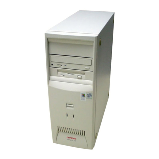
MECHANICAL DESIGN 2.3.1 CABINET LAYOUT Desktop Configuration Item NOTES: [1] All units may be configured as either a desktop or a minitower. Figure 2–2. Cabinet Layout, Front View Figure 2–3. Cabinet Layout, Rear View Minitower Configuration [1] Function Power On Light... -
Page 26: Chassis Layout
Chapter 2 System Overview 2.3.2 CHASSIS LAYOUT Audio Board (in ISA slot) [1] NOTE: [1] Audio board present only on CDS models. [2] Chassis fan only present on models using 66-MHz slot 1 (2-DIMM) system board. [3] 100-MHz slot 1 system board shown. Figure 2–4. -
Page 27: System Board Layout
2.3.3 SYSTEM BOARD LAYOUT 66-MHz Slot 1 (2-DIMM) System Board (ATX-type, P/N 008312-xxx) Item Function ISA expansion connectors CMOS Battery PCI expansion connectors AGP connector (J40) Serial connectors (J24): top, COM2; bottom, COM1 Parallel interface connector (J9) Mouse connector (J8) Keyboard connector (J7) Universal serial ports (J6): top, port B;... -
Page 28: System Architecture
Chapter 2 System Overview SYSTEM ARCHITECTURE The Compaq Deskpro EP Series of Personal Computers are based on Intel Celeron and Pentium II processors matched with a support chipset that is complimentary in design. The system architecture (Figure 2-6) utilizes three main buses: the Host bus, the Peripheral Component Interconnect (PCI) bus, and the Industry Standard Architecture (ISA) bus. -
Page 29: Figure 2-6. System Architecture
Graphics 32-Bit 66-MHz Cntlr. Card AGP Bus AGP Connector Ultra SCSI Ultra SCSI Controller Hard Drive Hard Drive IDE I/F Hard Drive Sec. IDE I/F Audio Audio Subsystem ISA Connector Keyboard/ Mouse I/F NOTES: [1] 3 PCI connectors on 66-MHz slot 1 system. 4 PCI connectors on 100-MHz slot 1 system. -
Page 30: Processor
Chapter 2 System Overview 2.4.1 PROCESSOR The Intel Celeron and Pentium II processors are backward-compatible with software written for x86-type and includes the dual-ALU central processing unit (CPU) with branch prediction support and an integrated L1 cache along with a math coprocessor. The Intel Celeron processor is a cost-efficient design with the Host bus interface operating at 66 MHz and no L2 cache. -
Page 31: Support Chipset
2.4.3 SUPPORT CHIPSET Table 2-2 shows the chipsets used for the Deskpro 2000 systems with MMX technology. Table 2–2. Support Chipsets Function North Bridge: Memory Controller Host/PCI Bridge Host/AGP Bridge South Bridge: PCI/ISA Bridge EIDE Controller DMA Controller Interrupt Controller Timer/Counter NMI Registers Reset Control Reg. -
Page 32: Universal Serial Bus Interface
Chapter 2 System Overview 2.4.6 UNIVERSAL SERIAL BUS INTERFACE This system features two Universal Serial Bus (USB) ports that provide a high speed interface for future systems and/or peripherals. The USB operates at 12 Mbps and provides hot plugging/unplugging (Plug ’n Play) functionality. 2.4.7 GRAPHICS SUBSYSTEM The graphics subsystem is contained on an AGP expansion board. -
Page 33: Specifications
Table 2–6. Physical Specifications Parameter Height Width Depth Weight NOTES: Metric measurements shown in parenthesis. [1] Desktop unit configured as minitower. Table 2-4. Environmental Specifications Operating to 95 F (10 to 35 C (no hard drive) 10,000 ft (3048 m) Table 2-5. - Page 34 Chapter 2 System Overview Table 2–7. Diskette Drive Specifications Diskette Drive Specifications Paramemter Media Type Height Bytes per Sector Sectors per Track: High Density Low Density Tracks per Side: High Density Low Density Read/Write Heads Average Access Time: Track-to-Track (high/low) Average (high/low) Settling Time Latency Average...
- Page 35 Table 2–9. Hard Drive Specifications Hard Drive Specifications Capacity Interface Drive Type Drive Size Transfer Rate Access Time (w/settling) Buffer Size Disk RPM Ultra DMA Support PIO Support SMART Level Support First Edition–- April1998 Technical Reference Guide Table 2-9. 2.1 GB 3.2 GB 6.4 GB EIDE...
- Page 36 Chapter 2 System Overview This page is intentionally blank. 2-14 Compaq Deskpro EP Series of Personal Computers First Edition – April 1998...
-
Page 37: Chapter 3 Processor/Memory Subsystem
Chapter 3 PROCESSOR/ MEMORY SUBSYSTEM Chapter 3 PROCESSOR/MEMORY SUBSYSTEM INTRODUCTION This chapter describes the processor/cache memory subsystem of the Compaq Deskpro EP Series of Personal Computers. Table 3-1 lists the key parameters of the processor/memory subsystem. Table 3–1. Processor/Memory Architectural Comparison North Bridge Host Bus (Slot 1) Frequency Cache Memory [1]:... -
Page 38: 66-Mh Zslot 1 Processor/Memory Subsystem
Chapter 3 Processor/Memory Subsystem 66-MHz SLOT 1 PROCESSOR/MEMORY SUBSYSTEM Systems using the 66-MHz slot 1 (2-DIMM) system board feature the Intel Celeron or Pentium II processor and employ the 82443EX system controller and 16 or 32 megabytes of system memory expandable to 256 megabytes. -
Page 39: Celeron Processor
3.2.1 CELERON PROCESSOR The Intel Celeron Processor (Figure 3-2) is contained on a PC board onto which is mounted a passive heat sink. The board installs into a Slot 1-type connector on the system board, allowing easy replacing/upgrading of the processor/cache memory complex. This processor includes a dual-ALU MMX-supporting CPU, branch prediction logic, dual-pipeline math coprocessor, and a 32-KB cache that is split into two 16-KB 4-way, set-associative caches for handling code and data separately. -
Page 40: Processor Changing/Upgrading
Chapter 3 Processor/Memory Subsystem 3.2.3 PROCESSOR CHANGING/UPGRADING The slot 1 design allows for easy changing and/or upgrading of the microprocessor/cache complex. NOTE: The Celeron processor-based system board employs retention uprights specifically designed for the Celeron processor board. The Pentium II processor-based system board can functionally accept the Celeron processor although the cartridge- retention uprights will not hold the Celeron processor board securely and could cause problems if the system unit is moved. -
Page 41: System Memory
3.2.4 SYSTEM MEMORY The 66-MHz slot 1 system board contains two 168-pin DIMM sockets for system memory. This system provides optimum performance with SDRAM DIMMs. As shipped from the factory the standard configuration has 32 megabytes of SDRAM installed and is expandable up to a maximum of 256 megabytes. - Page 42 Chapter 3 Processor/Memory Subsystem Table 3–3. SPD Address Map (SDRAM DIMM) Byte Description No. of Bytes Written Into EEPROM Total Bytes (#) In EEPROM Memory Type No. of Row Addresses On DIMM No. of Column Addresses On DIMM No. of Module Banks On DIMM 6, 7 Data Width of Module Voltage Interface Standard of DIMM...
-
Page 43: Figure 3-4. System Memorym
Figure 3-4 shows the system memory map for the system. FFFF FFFFh FFE0 0000h FFDF FFFFh FEC1 0000h FEC0 FFFFh FEC0 0000h FEBF FFFFh Host, PCI, AGP Area 4000 0000h 3FFF FFFFh 0100 0000h 00FF FFFFh Host, PCI, ISA Area 0010 0000h 000F FFFFh 000F 0000h... -
Page 44: Subsystem Configuration
Chapter 3 Processor/Memory Subsystem 3.2.5 SUBSYSTEM CONFIGURATION The 443EX component provides the configuration function for the processor/memory subsystem. Table 3-4 lists the configuration registers used for setting and checking such parameters as memory control and PCI bus operation. These registers reside in the PCI Configuration Space and accessed using the methods described in Chapter 4, section 4.2. -
Page 45: 100-Mh Zslot 1 Processor/Memory Subsystem
100-MHz SLOT 1 PROCESSOR/MEMORY SUBSYSTEM Systems using the 100-MHz slot 1 (3-DIMM) system board feature the 350- or 400-MHz Pentium II processor with an 82443BX system controller (north bridge) and 64 megabytes of system memory expandable to 384 megabytes (Figure 3-5). Pentium II SEC Cartridge (in Slot 1) - Page 46 Chapter 3 Processor/Memory Subsystem 3.3.1 PENTIUM II PROCESSOR The Intel Pentium II processor is packaged in a Single Edge Connector (SEC) cartridge that contains the microprocessor and 512-KB secondary (L2) cache (Figure 3-6). The cartridge installs into a Slot 1-type connector on the system board, allowing easy replacing/upgrading of the processor/cache memory complex.
- Page 47 3.3.1.2 Processor Changing/Upgrading The slot 1 design allows for easy changing and/or upgrading of the microprocessor/cache complex. The 100-MHz Slot 1 system board functionally supports all current Pentium II series processors. The mounting (retention) consideration for the Celeron processor is the same as that which is discussed in section 3.2.3.
- Page 48 Chapter 3 Processor/Memory Subsystem 3.3.2 SYSTEM MEMORY The 100-MHz slot 1system board contains three 168-pin DIMM sockets for system memory. This system is designed for using SDRAM DIMMs. As shipped from the factory the standard configuration has 64 megabytes of SDRAM installed. The system memory is expandable up to a maximum of 384 megabytes.
- Page 49 3.3.3 SUBSYSTEM CONFIGURATION The 443BX component provides the configuration function for the processor/memory subsystem. Table 3-6 lists the configuration registers used for setting and checking such parameters as memory control and PCI bus operation. These registers reside in the PCI Configuration Space and accessed using the methods described in Chapter 4, section 4.2.
- Page 50 Chapter 3 Processor/Memory Subsystem This page is intentionally blank. 3-14 Compaq Deskpro EP Series of Personal Computers First Edition - April 1998...
-
Page 51: Introduction
Chapter 4 SYSTEM SUPPORT 4. Chapter 4 SYSTEM SUPPORT INTRODUCTION This chapter covers subjects dealing with basic system architecture and covers the following topics: PCI bus overview (4.2) AGP bus overview (4.3) ISA bus overview (4.4) System clock distribution (4.5) Real-time clock and configuration memory (4.6) page 4-29 I/O map and register accessing (4.7) System management (4.8) -
Page 52: Pci Bus Overview
Chapter 4 System Support PCI BUS OVERVIEW NOTE: This section describes the PCI bus in general and highlights bus implementation in this particular system. For detailed information regarding PCI bus operation, refer to the PCI Local Bus Specification Revision 2.1. This system implements a 5-volt, 32-bit Peripheral Component Interconnect (PCI) bus operating at 33 MHz. -
Page 53: Pci Connector
4.2.1 PCI CONNECTOR Figure 4–2. PCI Bus Connector (32-Bit, 5V Type) Table 4–1. PCI Bus Connector Pinout B Signal A Signal -12 VDC TRST- +12 VDC +5 VDC +5 VDC +5 VDC INTA- INTB- INTC- INTD- +5 VDC PRSNT1- Reserved RSVD +5 VDC PRSNT2-... -
Page 54: Pci Bus Master Arbitration
Chapter 4 System Support 4.2.2 PCI BUS MASTER ARBITRATION The PCI bus supports a bus master/target arbitration scheme. A bus master is a device that has been granted control of the bus for the purpose of initiating a transaction. A target is a device that is the recipient of a transaction. -
Page 55: Pci Bus Transactions
4.2.3 PCI BUS TRANSACTIONS The PCI bus consists of a 32-bit path (AD31-00 lines) that uses a multiplexed scheme for handling both address and data transfers. A bus transaction consists of an address cycle and one or more data cycles, with each cycle requiring a clock (PCICLK) cycle. High performance is realized during burst modes in which a transaction with contiguous memory locations requires that only one address cycle be conducted and subsequent data cycles are completed using auto- incremented addressing. -
Page 56: Figure 4-3. Type 0 Configuration
Chapter 4 System Support Figure 4-3 shows how the loading of 0CF8h results in a Type 0 configuration cycle on the PCI bus. The Device Number (bits <15..11> determines which one of the AD31..11 lines is to be asserted high for the IDSEL signal, which acts as a “chip select” function for the PCI device to be configured. - Page 57 Table 4–4. PCI Function Configuration Acces Table 4-4. PCI Function Configuration Access PCI Function Host/PCI Bridge (82443) PCI/AGP Bridge (82443) PCI/ISA Bridge (82371) IDE Interface (82371) USB Interface (82371) Power Management Cntlr. (82371) The register index (CF8h, bits <7..2>)identifies the 32-bit location within the configuration space of the PCI device to be accessed.
-
Page 58: Option Rom Mapping
Chapter 4 System Support Table 4–5. PCI Device Identification PCI Device Identification PCI Device North Bridge (82443 PAC): Host/PCI Bridge (Function 0) [2] PCI/AGP Bridge (Function 1) South Bridge (82371 PIIX4): PCI/ISA Bridge (Function 0) EIDE Controller (Function 1) USB I/F (Function 2) Power Mngmt. -
Page 59: Pci Interrupt Mapping
4.2.5 PCI INTERRUPT MAPPING The PCI bus provides for four interrupt signals; INTA-, INTB-, INTC-, and INTD-. These signals may be generated by on-board PCI devices or by devices installed in the PCI slots. In order to minimize latency, INTA-..INTD- signal routing from the interrupt controller of the 82371south bridge to PCI slots/devices is distributed evenly as shown below: Interrupt Cntlr. -
Page 60: Pci Configuration
Chapter 4 System Support 4.2.7 PCI CONFIGURATION PCI bus operations, especially those that involve ISA bus interaction, require the configuration of certain parameters such as PCI IRQ routing, top of memory accessable by ISA, SMI generation, and clock throttling characteristics. These parameters are handled by the PCI/ISA bridge function (PCI function #0) of the south bridge component and configured through the PCI configuration space registers listed in Table 4-6. -
Page 61: Agp Bus Overview
AGP BUS OVERVIEW NOTE: This section describes the AGP bus in general. For a detailed description of AGP bus operations refer to the AGP Interface Specification available at the following AGP forum web site: http://www.agpforum.org/index.htm The Accelerated Graphics Port (AGP) bus is specifically designed as an economical yet a high- performance interface for 3D graphics adapters. - Page 62 Chapter 4 System Support 4.3.1.1 Data Request Requesting data is accomplished in one of two ways; either multiplexed addressing (using the AD lines for addressing/data) or demultiplexed (“sideband”) addressing (using the SBA lines for addressing only and the AD lines for data only). Even though there are only eight SBA lines (as opposed to the 32 AD lines) sideband addressing maximizes efficiency and throughput by allowing the AD lines to be exclusively used for data transfers.
- Page 63 AGP 2X Transfers In AGP 2X transfers clocking is basically the same as in 1X transfers except that the 66-MHz CLK signal is used to qualify only the control signals. The data bytes are latched by an additional strobe (AD_STBx) signal so that an 8-byte transfer occurs in one CLK cycle (Figure 4-6). The first four bytes (DnA) are latched by the receiving agent on the falling edge of AD_STBx and the second four bytes (DnB) are latched on the rising edge of AD_STBx.
-
Page 64: Agp Configuration
Chapter 4 System Support 4.3.2 AGP CONFIGURATION AGP bus operations require the configuration of certain parameters involving system memory access by the AGP graphics adapter. The AGP bus interface is configured as a PCI device integrated within the north bridge (82443, device 1) component. The AGP function is, from the PCI bus perspective, treated essentially as a PCI/PCI bridge and configured through PCI configuration registers (Table 4-7). -
Page 65: Agp Connector
4.3.3 AGP CONNECTOR Figure 4–7. AGP Bus Connector Table 4–8. AGP Bus Connector Pinout A Signal B Signal +12 VDC OVRCNT- RSVD USBN USBF INTA- INTB- RESET GNT- REQ- VDD3 VDD3 RSVD PIPE- RBF- RSVD RSVD SBA1 SBA0 VDD3 VDD3 SBA3 SBA2 RSVD... -
Page 66: Isa Bus Overview
Chapter 4 System Support ISA BUS OVERVIEW NOTE: This section describes the ISA bus in general and highlights bus implementation in this particular system. For detailed information regarding ISA bus operation, refer to the Compaq Extended Industry Standard Architecture (EISA) Technical Reference Guide. -
Page 67: Isa Expansionc
4.4.1 ISA CONNECTOR Figure 4–9. ISA Expansion Connector Table 4–9. ISA Expansion Connector Pinout 8-Bit ISA Interface Signal RESDRV +5 VDC IRQ9 -5 VDC DRQ2 -12 VDC NOWS- +12 VDC SMWTC- SMRDC- IOWC- IORC- DAK3- DRQ3 DAK1 DRQ1 REFRESH- BCLK IRQ7 IRQ6 IRQ5... -
Page 68: Isa Bus Transactions
Chapter 4 System Support 4.4.2 ISA BUS TRANSACTIONS The ISA bus supports 8- and 16-bit transfers at an 8-MHz rate. Devices limited to 8-bit transfers use the lower byte portion (data lines 7..0) while 16-bit transfers use the full bandwidth (data lines 15..0). - Page 69 Technical Reference Guide The following guidelines apply to optional ISA devices installed in the system: On bus lines that can be driven by a controller board, the driver should be able to sink a minimum of 20 ma at 0.5 VDC and source 2 ma at 3.75 VDC. On bus lines that are driven in the low direction only (open collector), the driver should be able to sink 20 ma at 0.5 VDC.
-
Page 70: Direct Memory Access
Chapter 4 System Support 4.4.3 DIRECT MEMORY ACCESS Direct Memory Access (DMA) is a method by which an ISA device accesses system memory without involving the microprocessor. DMA is normally used to transfer blocks of data to or from an ISA I/O device. DMA reduces the amount of CPU interactions with memory, freeing the CPU for other processing tasks. - Page 71 4.4.3.1 Page Registers The DMA page register contains the eight most significant bits of the 24-bit address and works in conjunction with the DMA controllers to define the complete (24-bit)address for the DMA channels. Table 4-11 lists the page register port addresses. Table 4–11.
- Page 72 Chapter 4 System Support The RAM refresh is designed to perform a memory read cycle on each of the 512 row addresses in the DRAM memory space. Refresh operations are used to refresh memory on the 32-bit memory bus and the ISA bus. The refresh address is provided on lines SA00 through SA08. Address lines LA23..17, SA18,19 are driven low.
-
Page 73: Interrupts
4.4.4 INTERRUPTS The microprocessor uses two types of interrupts; maskable and non-maskable. A maskable interrupt can be enabled or disabled within the microprocessor by the use of the STI and CLI instructions. A non-maskable interrupt cannot be masked off within the microprocessor but may be inhibited by hardware or software means external to the microprocessor. - Page 74 Chapter 4 System Support Table 4–13. Maskable Interrupt Priorities and Assignments Maskable Interrupt Priorities and Assignments Priority Signal Label IRQ0 IRQ1 IRQ8- IRQ9 IRQ10 IRQ11 IRQ12 IRQ13 IRQ14 IRQ15 IRQ3 IRQ4 IRQ5 IRQ6 IRQ7 IRQ2 Interrupts generated by PCI devices can be configured to share the standard AT (IRQn) interrupt lines.
- Page 75 4.4.4.2 Non-Maskable Interrupts Non-maskable interrupts cannot be masked (inhibited) within the microprocessor itself but may be maskable by software using logic external to the microprocessor. There are two nonmaskable interrupt signals: the NMI- and the SMI-. These signals have service priority over all maskable interrupts, with the SMI- having top priority over all interrupts including the NMI-.
- Page 76 Chapter 4 System Support SMI- Generation The SMI- (System Management Interrupt) is typically used for power management functions. When power management is enabled, inactivity timers are monitored. When a timer times out, SMI- is asserted and invokes the microprocessor’s SMI handler. The SMI- handler works with the APM BIOS to service the SMI- according to the cause of the timeout.
-
Page 77: Interval Timer
4.4.5 INTERVAL TIMER The interval timer generates pulses at software (programmable) intervals. A 8254-compatible timer is integrated into the South Bridge chip. The timer function provides three counters, the functions of which are listed in Table 4-15. Table 4–15. Interval Timer Functions Counter Function System Clock... -
Page 78: System Clock Distribution
Chapter 4 System Support SYSTEM CLOCK DISTRIBUTION Table 4-17 lists the system board clock signals and how they are distributed. Table 4–17. Clock Generation and Distribution Clock Generation and Distribution Frequncy/Signal Source 66, 100 MHz (CPUCLK) [1] 66 MHz North Bridge 48 MHz 33 MHz (PCICLK) 14.31818 MHz... -
Page 79: Real-Time Clock And Configuration Memory
REAL-TIME CLOCK AND CONFIGURATION MEMORY The Real-time clock (RTC) and configuration memory functions are provided by the 82371 South Bridge component. The RTC uses the first 14 of 256 bytes of configuration memory and is MC146818-compatible. As shown in the following figure, the 82371 provides 256 bytes of configuration memory (CMOS), divided into two 128-byte banks. -
Page 80: Configuration Memory Byte Definitions
Chapter 4 System Support 4.6.1 CONFIGURATION MEMORY BYTE DEFINITIONS Table 4-18 lists the mapping of the configuration memory. Table 4–18. Configuration Memory (CMOS) Map Location Function 00-0Dh Real-time clock Diagnostic status System reset code Diskette drive type Reserved Hard drive type Security functions Equipment installed Base memory size, low byte/KB... - Page 81 RTC Control Register A, Byte 0Ah Function Update in Progress. Read only. 0 = Time update will not occur before 2444 us 1 = Time update will occur within 2444 us 6..4 Divider Chain Control. R/W. 00x = Oscillator disabled. 010 = Normal operation (time base frequency = 32.768 KHz).
- Page 82 Chapter 4 System Support Configuration Byte 0Eh, Diagnostic Status Default Value = 00h This byte contains diagnostic status data. Configuration Byte 0Fh, System Reset Code Default Value = 00h This byte contains the system reset code. Configuration Byte 10h, Diskette Drive Type Function 7..4 Primary (Drive A) Diskette Drive Type...
- Page 83 Configuration Byte 13h, Security Functions Default Value = 00h Function Reserved QuickBlank Enable After Standby: 0 = Disable 1 = Enable Administrator Password: 0 = Not present 1 = Present Reserved Diskette Boot Enable: 0 = Enable 1 = Disable QuickLock Enable: 0 = Disable 1 = Enable...
- Page 84 Chapter 4 System Support Configuration Bytes 19h-1Ch, Hard Drive Types Byte 19h contains the hard drive type for drive 1 of the primary controller if byte 12h bits <7..4> hold 1111b. Byte 1Ah contains the hard drive type for drive 2 of the primary controller if byte 12h bits <3..0>...
- Page 85 Configuration Byte 26h, Auxiliary Peripheral Configuration Default Value = 00h Function I/O Delay Select 00 = 420 ns (default) 01 = 300 ns 10 = 2600 ns 11 = 540 ns Alternative A20 Switching 0 = Disable port 92 mode 1 = Enable port 92 mode Bi-directional Print Port Mode 0 = Disabled...
- Page 86 Chapter 4 System Support Configuration Byte 29h, Miscellaneous Configuration Data Default Value = 00h Function 7..5 Reserved Primary Hard Drive Enable (Non-PCI IDE Controllers) 0 = Disable 1 = Enable 3..0 Reserved Configuration Byte 2Ah, Hard Drive Timeout Default Value = 02h Function 7..5 Reserved...
- Page 87 Configuration Byte 2Dh, Additional Flags Default Value = 00h Function 7..5 Reserved Memory Test 0 = Test memory on power up only 1 = Test memory on warm boot POST Error Handling (BIOS Defined) 0 = Display “Press F1 to Continue” on error 1 = Skip F1 message 2..0 Reserved...
- Page 88 Chapter 4 System Support Configuration Byte 35h, APM Status Flags Default Value = 11h Function 7..6 Power Conservation State: 00 = Ready 01 = Standby 10 = Suspend 11 = Off Reserved 32-bit Connection: 0 = Disconnected, 1 = Connected 16-bit Connection 0 = Disconnected, 1 = Connected Real Mode Connection...
- Page 89 Configuration Byte 45h, Keyboard Snoop Data Default Value = xxh Function Cntrl/F10 Key Status: 0 = Cntrl & F10 keys not pressed 1 = Cntrl & F10 keys pressed F10 Key Status: 0 = F10 key not pressed 1 = F10 key pressed 5..1 Reserved Key Pressed Flag:...
- Page 90 Chapter 4 System Support Configuration Byte 52h, Board Revision This byte holds the board revision as copied from the boot block sector. Configuration Byte 53h, 54h, SW SMI Command/Data Bytes Configuration Byte 55h, APM Command Byte Configuration Byte 56h, Miscellaneous Flags Byte Function CAS Latency: 0 = 2, 1 = 3...
- Page 91 Configuration Byte 83h, Microprocessor Identification This byte holds the component ID and chip revision of the microprocessor. Configuration Byte 84h, Microprocessor Revision Configuration Byte 85h, Administration Mode Function Reserved ESCD Buffering: 0 = No buffering, 1 = ESCD buffered at F000h. Hood Lock Enable: 0 = Disabled, 1 = Enabled User Mode Flag...
- Page 92 Chapter 4 System Support Configuration Byte 90h, 91h, Total Super Extended Memory Configured This byte holds the value of the amount of extended system memory that is configured. The amount is given in 64-KB increments. Configuration Byte 92h, Miscellaneous Configuration Byte Default Value = 18h Function 7..5...
- Page 93 Configuration Byte 94h, ROM Flash/Power Button Status Default Value = 00h Function 7..5 Reserved ROM Flash In Progress (if set) Reserved Power Button Inhibited (ifset) User-Forced Bootblock (if set) ROM Flash In Progress (if set) Configuration Byte 97h, Asset/Test Prompt Byte Default Value = 00h Function Test Prompt:...
- Page 94 Chapter 4 System Support Configuration Byte 9Dh, ESS Audio Configuration Byte Default Value = 12h Function Reserved for Game Port Enable Audio Address 00 = 22xh 01 = 23xh 10 = 24xh 11 = 25xh DMA Channel 00 = Disabled 01 = DMA0 10 = DMA1 11 = DMA3...
- Page 95 Configuration Byte C7h, C8h, Serial Ports 1 and 2 (Respectively) Configuration Bytes Default Value = FEh, 7Dh Function 7..2 Base I/O Address (in packed format) (Algorithm: [Addr. - 200h] / 8) (i.e., 3Fh = 3F8h, 1Fh = 2F8h, 00 = 200h) 1..0 Interrupt: 00 = Reserved...
-
Page 96: I/O Map And Register Accessing
Chapter 4 System Support I/O MAP AND REGISTER ACCESSING 4.7.1 SYSTEM I/O MAP Table 4–19. System I/O Map I/O Port Function 0000..000Fh DMA Controller 1 0020..0021h Interrupt Controller 1 0040..0043h Timer 1 0060h Keyboard Controller Data Byte 0061h NMI, Speaker Control 0064h Keyboard Controller Command/Status Byte 0070h... -
Page 97: 82371 South Bridge Gpio Configuration
4.7.2 82371 SOUTH BRIDGE GPIO CONFIGURATION The 82371 South Bridge component includes a number of single and dual purpose pins available as general purpose input/output (GPIO) ports. The GPIO ports are configured during POST by BIOS through the PCI configuration registers B0-B3h (82371, function 0). Tables 4-20 and 4-21 list the utilization of the GPIO ports in this system. - Page 98 Chapter 4 System Support Table 4–21. 82371 South Bridge General Purpose Output Port Utilization 82371 South Bridge General Purpose Output Port Utilization GP Output Port Function GPO #0 PCI reset. When low will generate a PCI RST- to PCI slots. GPO #1-7 ISA bus address signals LA17-23.
-
Page 99: 87309 I/O Controller Configuration
4.7.3 87309 I/O CONTROLLER CONFIGURATION The 87309 I/O controller contains various functions such as the keyboard/mouse interfaces, diskette interface, serial interfaces, and parallel interface. While the control of these interfaces uses standard AT-type I/O addressing, the configuration of these functions uses indexed ports unique to the 87307. -
Page 100: System Management Support
Chapter 4 System Support SYSTEM MANAGEMENT SUPPORT This section describes the hardware support of functions involving security, safety, identification, and power consumption of the system. The following sections describe the system management functions. Any BIOS interaction required of these functions is described in Chapter 7, “BIOS ROM.”... -
Page 101: I/O Security
4.8.3 I/O SECURITY The 87309 I/O controller allows various I/O functions (serial, parallel, diskette I/O) to be disabled through configuration registers. 4.8.4 POWER MANAGEMENT This system provides baseline hardware support of ACPI- and APM-compliant firmware and software. The major power-consuming components (processor, chipset, I/O controller, and fan) can be placed into a reduced power mode upon software command either automatically or by user control. -
Page 102: Monitor Power Control
Chapter 4 System Support 4.8.4.3 HARD DRIVE SPINDOWN CONTROL The timeout parameter stored in the SIT record 04h and indexed through CMOS location 2Ah (bits <4..0>) represents the period of hard drive inactivity required to elapse before the hard drive is allowed to spin down. -
Page 103: Chapter 5 Input/Output Interfaces
Chapter 5 INPUT/OUTPUT INTERFACES Chapter 5 INPUT/OUTPUT INTERFACES INTRODUCTION This chapter describes the system’s interfaces that provide input and output (I/O) porting of data and specifically discusses interfaces that are controlled through I/O-mapped registers. The I/O interfaces are functions integrated into the south bridge and 87309 components. The following I/O interfaces are covered in this chapter: Enhanced IDE (EIDE) interface (5.2) Diskette drive interface (5.3) - Page 104 Chapter 5 Input/Output Interfaces 5.2.1.1 IDE Configuration Registers The configuration registers of the IDE controller are integrated into the south bridge (82371EB) component and configured as a PCI device with bus mastering capability. The PCI configuration registers for the IDE controller function (PCI device #20, function #1) are listed in Table 5-1. Table 5–1.
- Page 105 5.2.1.2 IDE Bus Master Control Registers The IDE interface supports drives that can operate using Ultra ATA protocol by initiating PCI bus master operations using the I/O mapped control registers listed in Table 5-2. Table 5–2. IDE Bus Master Control Registers IDE Bus Master Control Registers I/O Addr.
- Page 106 Chapter 5 Input/Output Interfaces 5.2.1.3 IDE ATA Control Registers The IDE controller decodes the addressing of the standard AT attachment (ATA) registers for the connected IDE drive, which is where the ATA control registers actually reside. The primary and secondary interface connectors are mapped as shown in Table 5-3. Table 5–3.
- Page 107 The contents of the Error register are interpreted as a diagnostic status byte after the execution of a diagnostic command or when the system is initialized. Function Bad Block Mark Detected in Requested Sector ID Field (if set) Non-correctable Data Error (if set) Reserved Requested Sector ID Field Not Found (if set) Reserved...
- Page 108 Chapter 5 Input/Output Interfaces Drive Select/Head Register, I/O Port 1F6h/176h Function Reserved Sector Size: 00 = Reserved 01 = 512 bytes/sector 10, 11 = Reserved Drive Select: 0 = Drive 1 1 = Drive 2 3..0 Head Select Number: 0000 = 0 1000 = 8 0001 = 1 1001 = 9...
- Page 109 Command Register, I/O Port 1F7h/177h (Write Only) The IDE controller commands are written to this register. The command write action should be prefaced with the loading of data into the appropriate registers. Execution begins when the command is written to 1F7h/177h. Table 5-4 lists the standard IDE commands. Table 5–4.
- Page 110 Chapter 5 Input/Output Interfaces Drive Control Register, I/O Port 3F6h/376h (Write Only) Function 7..3 Reserved Controller Control: 0 = Re-enable 1 = Reset Interrupt Enable/Disable 0 = Disable interrupts 1 = Enable interrupts Reserved Drive Access Register, I/O Port 3F7h/377h (Read Only) Function Reserved WRITE GATE- Signal Active (if set)
-
Page 111: Ide Connector
5.2.2 IDE CONNECTOR This system uses a standard 40-pin connector for IDE devices. Device power is supplied through a separate connector. Figure 5–1. 40-Pin IDE Connector. Table 5–5. 40-Pin IDE Connector Pinout Signal Description RESET- Reset Ground Data Bit <7> Data Bit <8>... -
Page 112: Diskette Drive Interface
Chapter 5 Input/Output Interfaces DISKETTE DRIVE INTERFACE The diskette drive interface supports up to two diskette drives through a standard 34-pin diskette drive connector. All models come standard with a 3.5 inch 1.44-MB diskette drive installed as drive A. An additional diskette drive may be installed, requiring an optional three-connector diskette drive cable. -
Page 113: Diskette Drive Programming
5.3.1 DISKETTE DRIVE PROGRAMMING 5.3.1.1 Diskette Drive Interface Configuration The diskette drive controller must be configured for a specific address and also must be enabled before it can be used. Address selection and enabling of the diskette drive interface are affected by firmware through the PnP configuration registers of the 87309 I/O controller. -
Page 114: Table 5-7. Diskette Drivec
Chapter 5 Input/Output Interfaces 5.3.1.2 Diskette Drive Interface Control The BIOS function INT 13 provides basic control of the diskette drive interface. The diskette drive interface can be controlled by software through I/O-mapped registers listed in Table 5-7. Table 5–7. Diskette Drive Controller Registers Diskette Drive Interface Control Registers Primary Alternate... - Page 115 Main Status Register, I/O Port 3F4h/374h (Read Only) Function Request for Master. When set, indicates the controller is ready to send or receive data from the CPU. Cleared immediately after a byte transfer. Indicates interrupt pin status during non- DMA phase. Data I/O Direction.
-
Page 116: Diskette Drive Connector
Chapter 5 Input/Output Interfaces 5.3.2 DISKETTE DRIVE CONNECTOR This system uses a standard 34-pin connector (refer to Figure 5-2 and Table 5-8 for the pinout) for diskette drives. Drive power is supplied through a separate connector. Figure 5–2. 34-Pin Diskette Drive Connector. Table 5–8. -
Page 117: Serial Interface
SERIAL INTERFACE The serial interface transmits and receives asynchronous serial data with external devices. The serial interface function is provided by the 87309 I/O controller component, which integrates a 16550/16450-compatible UART. The UART is paired with a DB-9 connector and complies with the RS-232 standard. -
Page 118: Serial Interface Programming
Chapter 5 Input/Output Interfaces 5.4.2 SERIAL INTERFACE PROGRAMMING 5.4.2.1 Serial Interface Configuration The serial interfaces must be configured for a specific address range (COM1, COM2, etc.) and also must be activated before it can be used. Address selection and activation of the serial interface are affected through the PnP configuration registers of the 87309 I/O controller. -
Page 119: Table 5-11. Serial Interface
5.4.2.2 Serial Interface Control The BIOS function INT 14 provides basic control of the serial interface. The serial interface can be controlled by software through the registers listed in Table 5-11. Table 5–11. Serial Interface Control Registers Serial Interface Control Registers Address Register Base... - Page 120 Chapter 5 Input/Output Interfaces Baud Rate Divisor Latch Register, I/O Port 3F8h, 3F9h/2F8, 2F9h When bit <7> of the Line Control register is set (1), a write to this pair of locations loads the decimal value used to divide the 1.8462-MHz clock to create the desired baud rate for serial transmission.
- Page 121 FIFO Control Register, I/O Port 3FAh/2FAh (Write Only) This write-only register enables and clears the FIFOs and set the trigger level and DMA mode. Function Receiver Trigger Level 00 = 1 byte 10 = 8 bytes 01 = 4 bytes 11 = 14 bytes 5..3 Reserved...
- Page 122 Chapter 5 Input/Output Interfaces Line Status Register, I/O Port 3FDh/2FDh (Read Only) This register contains the status of the current data transfer. Bits <2..0> are cleared when read. Function Parity Error, Framing Error, or Break Cond. Exists (if set) TX Holding Reg. and Transmitter Shift Reg. Are Empty (if set) TX Holding Reg.
-
Page 123: Parallel Interface
PARALLEL INTERFACE The parallel interface provides connection to a peripheral device that has a compatible interface, the most common being a printer. The parallel interface function is integrated into the 87309 I/O controller component and provides bi-directional 8-bit parallel data transfers with a peripheral device. -
Page 124: Enhanced Parallel Port Mode
Chapter 5 Input/Output Interfaces 5.5.2 ENHANCED PARALLEL PORT MODE In Enhanced Parallel Port (EPP) mode, increased data transfers are possible (up to 2 MB/s) due to a hardware protocol that provides automatic address and strobe generation. EPP revisions 1.7 and 1.9 are both supported. For the parallel interface to be initialized for EPP mode, a negotiation phase is entered to detect whether or not the connected peripheral is compatible with EPP mode. -
Page 125: Parallel Interface Programming
5.5.4 PARALLEL INTERFACE PROGRAMMING 5.5.4.1 Parallel Interface Configuration The parallel interface must be configured for a specific address range (LPT1, LPT2, etc.) and also must be enabled before it can be used. When configured for EPP or ECP mode, additional considerations must be taken into account. -
Page 126: Table 5-12. Parallel Interface
Chapter 5 Input/Output Interfaces 5.5.4.2 Parallel Interface Control The BIOS function INT 17 provides simplified control of the parallel interface. Basic functions such as initialization, character printing, and printer status are provide by subfunctions of INT 17. The parallel interface is controllable by software through a set of I/O mapped registers. The number and type of registers available depends on the mode used (SPP, EPP, or ECP). - Page 127 Status Register, I/O Port 379h, Read Only This register contains the current printer status. Reading this register clears the interrupt condition of the parallel port. Function Printer Busy (if 0) Printer Acknowledgment Of Data Byte (if 0) Printer Out Of Paper (if 1) Printer Selected/Online (if 1) Printer Error (if 0) Reserved...
- Page 128 Chapter 5 Input/Output Interfaces FIFO Register, I/O Port 7F8h (ECP Mode Only) While in ECP/forward mode, this location is used for filling the 16-byte FIFO with data bytes. Reads have no effect (except when used in Test mode). While in ECP/backward mode, reads yield data bytes from the FIFO.
-
Page 129: Parallel Interface Connector
5.5.5 PARALLEL INTERFACE CONNECTOR Figure 5-4 and Table 5-14 show the connector and pinout of the parallel interface connector. Figure 5–4. Parallel Interface Connector (Female DB-25 as viewed from rear of chassis) Table 5–14. DB-25 Parallel Connector Pinout Signal Description STB- Strobe Data 0... -
Page 130: Keyboard/Pointing Device Interface
Chapter 5 Input/Output Interfaces KEYBOARD/POINTING DEVICE INTERFACE The keyboard/pointing device interface provides the connection of an enhanced keyboard and a mouse using PS/2-type connections. The keyboard/pointing device interface function is provided by the 87309 I/O controller component, which integrates 8042-compatible keyboard controller logic (hereafter referred to as simply the “8042”) to communicate with the keyboard and pointing device using bi-directional serial data transfers. -
Page 131: 8042-T O -Keyboard
Control of the data and clock signals is shared by the 8042and the keyboard depending on the originator of the transferred data. Note that the clock signal is always generated by the keyboard. After the keyboard receives a command from the 8042, the keyboard returns an ACK code. If a parity error or timeout occurs, a Resend command is sent to the 8042. -
Page 132: Pointing Device Interface Operation
Chapter 5 Input/Output Interfaces 5.6.2 POINTING DEVICE INTERFACE OPERATION The pointing device (typically a mouse) connects to a 6-pin DIN-type connector that is identical to the keyboard connector both physically and electrically. The operation of the interface (clock and data signal control) is the same as for the keyboard. The pointing device interface uses the IRQ12 interrupt. - Page 133 5.6.3.2 8042 Control The BIOS function INT 16 is typically used for controlling interaction with the keyboard. Sub- functions of INT 16 conduct the basic routines of handling keyboard data (i.e., translating the keyboard’s scan codes into ASCII codes). The keyboard/pointing device interface is accessed by the CPU through I/O mapped ports 60h and 64h, which provide the following functions: Output buffer reads Input buffer writes...
- Page 134 Chapter 5 Input/Output Interfaces Table 5-17 lists the commands that can be sent to the 8042 by the CPU. The 8042 uses IRQ1 for gaining the attention of the CPU. Table 5–17. CPU Commands To The 8042 Value Command Description Put current command byte in port 60h.
- Page 135 Table 5-17. CPU Commands To The 8042 (Continued) Value Command Description Read input port of the 8042. This command directs the 8042 to transfer the contents of the input port to the output buffer so that they can be read at port 60h. The contents are as follows: Bit <7>...
-
Page 136: Keyboard/Pointing Dfevice Interface Connector
Chapter 5 Input/Output Interfaces 5.6.4 KEYBOARD/POINTING DFEVICE INTERFACE CONNECTOR There are separate connectors for the keyboard and pointing device. Both connectors are identical both physically and electrically. Figure 5-6 and Table 5-18 show the connector and pinout of the keyboard/pointing device interface connectors. Figure 5–6. -
Page 137: Universal Serial Bus Interface
UNIVERSAL SERIAL BUS INTERFACE The Universal Serial Bus (USB) interface provides up to 12 Mb/s data transfers between the host system and peripherals designed with a compatible USB interface. This high speed interface supports hot-plugging of compatible devices, making possible system configuration changes without powering down or even rebooting systems. -
Page 138: Usb Control
Chapter 5 Input/Output Interfaces 5.7.3 USB CONTROL The USB is controlled through I/O registers as listed in table 5-20. Table 5–20. USB Control Registers USB Control Registers I/O Addr. Register 00, 01h Command 02, 03h Status 04, 05h Interupt Enable 06, 07 Frame No. -
Page 139: Chapter 6 Power And Signal Distribution
Chapter 6 POWER and SIGNAL DISTRIBUTION 6. Chapter 6 Power and Signal Distribution INTRODUCTION This chapter describes the power supply and method of general power and signal distribution in the Compaq Deskpro CONTACT Personal Computer. Topics covered in this chapter include: Power supply assembly/control (6.2) Power distribution (6.3) General signal distribution (6.4) -
Page 140: Power Supply Assembly
Chapter 6 Power and Signal Distribution 6.2.1 POWER SUPPLY ASSEMBLY The power supply assembly is contained in a single unit that features a selectable input voltage: 90-132 VAC and 180-264 VAC. The power supply assembly provides +3.3 VDC, +5 VDC, -5 VDC, +12 VDC, and -12 VDC potentials for the system board, expansion board(s), and installed drives. -
Page 141: Power Control
6.2.2 POWER CONTROL The power supply assembly is controlled digitally by the PS On signal (Figure 6-1). When PS On is asserted, the power supply assembly is activated and all voltage outputs (+3 VDC, +5 AUX, +/- 5 VDC, +/-12 VDC) are produced. When PS On is de-asserted, the power supply assembly is off and all voltages (except +5 AUX) are not generated. -
Page 142: Wake Up Events
Chapter 6 Power and Signal Distribution 6.2.2.3 Power Restore Feature The system includes a power restore feature. A circuit powered by the RTC/CMOS battery holds the state of the PS On signal so that if a power outage occurs the system, when power is regained, will revert to the power state of the system at the time power was lost. -
Page 143: Power Distribution
POWER DISTRIBUTION 6.3.1 3/5/12 VDC DISTRIBUTION The power supply assembly includes a multi-connector cable assembly that routes +3.3 VDC, +5 AUX, +5 VDC, -5 VDC, +12 VC, and -12 VDC to the system board and +/-5 and +/-12 to the individual drive assemblies. -
Page 144: Low Voltage Distribution
Chapter 6 Power and Signal Distribution 6.3.2 LOW VOLTAGE DISTRIBUTION Voltages less than 3.3 VDC and the processor core voltage are produced through regulator circuitry on the system board. Power Supply VID0 VID1 VID2 Processor VID3 VID4 Figure 6–3. Low Voltage Regulator Circuitry, Block Diagram The VccP regulator produces the VccP (processor core) voltage according to the state of the VID4..0 signals from the Pentium II processor. -
Page 145: General Signal Distribution
GENERAL SIGNAL DISTRIBUTION Figure 6-4 shows general signal distribution between the main subassemblies of the system unit. Figure 6-5 shows the pinout of the front bezel control/indicator connector. Figure 6-6 shows the pinout of the Wake-On-LAN connector. Graphics Audio Controller Controller (AGP Card) (ISA Card) -
Page 146: Figure 6-5. Front Panel
Chapter 6 Power and Signal Distribution Header P5 NOTE: [1] Pins 8 and 9 allow a SCSI hard drive to drive the HD Activity LED, which in the standard configuration is driven from an IDE drive. Figure 6–5. Front Panel (Bezel) Control/Indicator Connector Header P9 Figure 6–6. -
Page 147: Chapter 7 Bios Rom
Chapter 7 BIOS ROM 7. Chapter 7 BIOS ROM INTRODUCTION The Basic Input/Output System (BIOS) of the computer is a collection of machine language programs stored as firmware in read-only memory (ROM). The BIOS ROM includes such functions as Power-On Self Test (POST), PCI device initialization, Plug ‘n Play support, and power management support including APM 1.2, and ACPI. -
Page 148: Boot Functions
Chapter 7 BIOS ROM BOOT FUNCTIONS The system supports new system boot functions to support remote ROM flashing and PC97 requirements. 7.2.1 BOOT BLOCK This system includes 24 KB of boot block ROM that provides a way to recover from a failed remote flashing of the system BIOS ROM. -
Page 149: Memory Detection And Configuration
MEMORY DETECTION AND CONFIGURATION This system uses the Serial Presence Detect (SPD) method of determining the installed DIMM configuration. The BIOS communicates with an EEPROM on each DIMM through an I bus to obtain data on the following DIMM parameters: Presence Size Type... -
Page 150: Client Management Support
Chapter 7 BIOS ROM CLIENT MANAGEMENT SUPPORT Client Management deals with issues of security, identification, and system management functions. Client Management is provided through BIOS INT15 functions listed Table 7-1. Table 7–1. PnP Client Management Functions (INT15) Client Management Functions (INT15) Function E800h Get system ID... - Page 151 To support Windows NT an additional table to the BIOS32 table has been defined to contain 32- bit pointers for the DDC and SIT locations. The Windows NT extension table is as follows: ; Extension to BIOS SERVICE directory table (next paragraph) “32OS”...
-
Page 152: System Id/Revision/Serial No
Chapter 7 BIOS ROM 7.4.1 SYSTEM ID/REVISION/SERIAL NO. The INT 15, AX=E800h BIOS function can be used to identify the system board. The system ID will be returned in the BX register as follows: System 66-MHz slot 1 (2-DIMM socket) 100-MHz slot 1 (3-DIMM socket) The INT 15, AX=E814h BIOS function retrieves the system board revision. - Page 153 Timeout Counter Record (Video Screensave), SIT Record 03h Byte [1] Function Record ID for Video Screensave Timeout No. of Data Bytes in Record First Value Last Value Security Record, SIT Record 05h Byte Function Record ID No. of Data Bytes in Record NVRAM/HD Lock, QuickLock/QuickBlank, FD Boot, PWR Pwd Virus Detect, Serial/Parallel Cntrl., FD Drive Cntl., Stby Cntrl.
- Page 154 Chapter 7 BIOS ROM Peripheral and Input Device Record, SIT Record 07h Byte Function Record ID No. of Data Bytes in Record DMA Functions, SCSI Support, Flashable ROM, Setup Partition, 101 Keyboard Erase-Eaze Kybd. Support in ROM, El Torito CD Boot Support, QuickBoot, ROM Functions Form factor Softdrive 1 &...
- Page 155 Memory Module Information Record, SIT Record 08h Byte Function Record ID No. of Data Bytes in Record No. of Sockets Memory Socket Location 0 Memory Installed In Location 0 Memory Speed In Location 0 Memory Form Factor 0 Memory Socket Location 1 Memory Installed In Location 1 Memory Speed In Location 1 Memory Form Factor 1...
- Page 156 Chapter 7 BIOS ROM Extended Disk Support Record, SIT Record 0Eh Byte Function Record ID No. of Data Bytes in Record Pointer To Extended Disk table (High Byte) Pointer To Extended Disk table (Low Byte) NOTE: [1] Determined at runtime. System Record, SIT Record 0Fh (Not Used) Product Name Header Record, SIT Record 10h Byte...
- Page 157 DMI System Slots Support Record, SIT Record 16h Byte Function Record ID No. of Data Bytes in Record Number of Slots Type of Slot Data Width of Slot Slot Usage/Length/Virtual Slot Category Slot ID Type of Slot Data Width of Slot Slot Usage/Length/Virtual Slot Category Slot ID...
-
Page 158: Edid Retrieve
Chapter 7 BIOS ROM 7.4.3 EDID RETRIEVE The BIOS function INT 15, AX=E813h is a tri-modal call that retrieves the VESA extended display identification data (EDID). Two subfunctions are provided: AX=E813h BH=00h retrieves the EDID information while AX=E813h BX=01h determines the level of DDC support. Input: = E813h = 00 Get EDID . -
Page 159: System Map Retrieval
7.4.5 SYSTEM MAP RETRIEVAL The BIOS function INT 15, AX=E820h will return base memory and ISA/PCI memory contiguous with base memory as normal memory ranges. This real mode call will indicate chipset-defined address holes not in use, motherboard memory-mapped devices, and all occurrences of the system BIOS as reserved. -
Page 160: Flash Rom Functions
Chapter 7 BIOS ROM 7.4.6 FLASH ROM FUNCTIONS The system BIOS may be upgraded by flashing the ROM using the INT 15, AX=E822h BIOS interface, which includes the necessary subfunctions. Upgrade by flashing is provided by a ROMPAQ diskette. The upgrade procedure is described at the end of this chapter. Corrupted BIOS code will be indicated by the keyboard LEDs as described previously in section 7.2.1. - Page 161 The INT 15, AX=E822h, BL=09h function is used to restore the power button to the state it was in prior to invoking the Disable (BL=08h) function. Entry: = E822h = 09h = 00 (Failure) = 86, call not supported First Edition- April 1998 Technical Reference Guide Compa Deskpro EP Series of Personal Computers 7-15...
-
Page 162: Accessing Cmos
Chapter 7 BIOS ROM 7.4.8 ACCESSING CMOS Configuration memory data can be retrieved with the BIOS call INT 15, AX=E823h. This tri- modal function retrieves a single byte from the CMOS map described in Chapter 4. The function is described as follows: INPUT: = E823h = 0, Read... - Page 163 Function 0000h PCI 2.1 Mode (Enabled) 0001h Erase Eaze Keyboard (off) 0002h Comm/IR Port Designation (Comm port) 0003h No Rejection of SETs By PnP (reject SETs) 0004h PCI VGA Snoop (snoop disabled) 0005h PCI Bus Mastering BIOS Support (enabled) 0006h Auto Prompt for Auto Setup (prompt for F1, F2, F10) 0007h Mode 2 Configuration Support (enabled)
-
Page 164: Security Functions
Chapter 7 BIOS ROM 7.4.10 SECURITY FUNCTIONS The INT 15 AX=E846h BIOS function is used to control various security features of the system. This function may be issued by a remote system (over a network). The issuing driver must build a request buffer for each security feature prior to making the call. -
Page 165: Pnp Support
PnP SUPPORT The BIOS includes Plug ’n Play (PnP) support for PnP version 1.0A. NOTE: For full PnP functionality to be realized, all peripherals used in the system must be designed as “PnP ready.” Any installed ISA peripherals that are not “PnP ready” can still be used in the system, although configuration parameters may need to be considered (and require intervention) by the user. -
Page 166: Smbios
Chapter 7 BIOS ROM 7.5.1 SMBIOS In support of the DMI specification the PnP functions 50h and 51h are used to retrieve the SMBIOS data. Function 50h retrieves the number of structures, size of the largest structure, and SMBIOS version. Function 51h retrieves a specific structure. This system supports SMBIOS version 2.1 and the following structure types: Type Data... -
Page 167: Power Management Functions
POWER MANAGEMENT FUNCTIONS The BIOS ROM provides three types of power management support; independent PM support, APM support, and ACPI support. 7.6.1 INDEPENDENT PM SUPPORT The BIOS ROM can provide power management of the system independently from any software (OS or application) that is running on the system. In this mode the BIOS uses a timer to determine when to switch the system to a different power state. -
Page 168: Apm Support
Chapter 7 BIOS ROM 7.6.3 APM SUPPORT Advanced Power Management (APM) BIOS support provides interaction between the BIOS ROM and the operating system (OS). The BIOS advises the OS when a power state transition should occur. The OS then notifies the appropriate driver(s) and reports back to the BIOS. For maximum energy-conservation benefit, APM functionality should be implemented using the following three layers: BIOS layer (APM BIOS (ver. - Page 169 Standby - The computer is in a low power state: video is off, some subsystems may be drawing less power, and the microprocessor is halted except for servicing interrupts. Video graphics controller is under driver control and/or VSYNC is off and the power supply fan is turned off. Any of the following activities will generate a wake-up SMI and return the system to On: Keyboard Mouse...
-
Page 170: Usb Legacy Support
Chapter 7 BIOS ROM USB LEGACY SUPPORT The BIOS ROM checks the USB port, during POST, for the presence of a USB keyboard. This allows a system with only a USB keyboard to be used during ROM-based setup and also on a system with an OS that does not include a USB driver. -
Page 171: Appendix A Error Messages And Codes
Appendix A ERROR MESSAGES AND CODES A. Appendix A ERROR MESSAGES AND CODES INTRODUCTION This appendix lists the error codes and a brief description of the probable cause of the error. Note that not all errors listed in this appendix may be applicable to a particular system depending on the model and/or configuration. -
Page 172: Power-On Self Test (Post) Messages
Appendix A Error Messages and Codes POWER-ON SELF TEST (POST) MESSAGES Table A–3. Power-On Self Test (POST) Messages Error Message Bad PnP Serial ID Checksum Address Lines Short! Cache Memory Failure, Do Not Enable Cache! CMOS Battery Failed CMOS Checksum Invalid CMOS System Options Not Set CMOS Display Type Mismatch CMOS Memory Size Mismatch... -
Page 173: Processor Error Messages
PROCESSOR ERROR MESSAGES (1xx-xx) Table A–4. Processor Error Messages Message Probable Cause 101-01 CPU test failed 101-02 32-bit CPU test failed 101-91..94 Multiplication test failed 102-01 FPU initial sts. word incorrect 102-02 FPU initial cntrl. Word incorrect 102-03 FPU tag word not all ones 102-04 FPU tag word not all zeros 102-05... -
Page 174: Memory Error Messages
Appendix A Error Messages and Codes MEMORY ERROR MESSAGES (2xx-xx) Table A–5. Memory Error Messages Memory Error Messages Message Probable Cause 200-04 Real memory size changed 200-05 Extended memory size changed 200-06 Invalid memory configuration 200-07 Extended memory size changed 200-08 CLIM memory size changed 201-01... -
Page 175: Printer Error Messages
PRINTER ERROR MESSAGES (4xx-xx) Table A–7. Printer Error Messages Message Probable Cause 401-01 Printer failed or not connected 402-01 Printer data register failed 402-02 Printer control register failed 402-03 Data and control registers failed 402-04 Loopback test failed 402-05 Loopback test and data reg. failed 402-06 Loopback test and cntrl. -
Page 176: Diskette Drive Error Messages
Appendix A Error Messages and Codes A.10 DISKETTE DRIVE ERROR MESSAGES (6xx-xx) Table A–9. Diskette Drive Error Messages Message Probable Cause 6xx-01 Exceeded maximum soft error limit 6xx-02 Exceeded maximum hard error limit 6xx-03 Previously exceeded max soft limit 6xx-04 Previously exceeded max hard limit 6xx-05 Failed to reset controller... -
Page 177: Modem Communications Error Messages
A.12 MODEM COMMUNICATIONS ERROR MESSAGES (12xx-xx) Table A–11. Serial Interface Error Messages Message Probable Cause 1201-XX Modem internal loopback test 1201-01 UART DLAB bit failure 1201-02 Line input or UART failure 1201-03 Address line failure 1201-04 Data line fault 1201-05 UART control signal failure 1201-06 UART THRE bit failure... -
Page 178: Hard Drive Error Messages
Appendix A Error Messages and Codes A.13 HARD DRIVE ERROR MESSAGES (17xx-xx) Table A–12. Hard Drive Error Messages Message Probable Cause 17xx-01 Exceeded max. soft error limit 17xx-02 Exceeded max. Hard error limit 17xx-03 Previously exceeded max. soft error limit 17xx-04 Previously exceeded max.hard error limit 17xx-05... -
Page 179: Hard Drive Error Messages
A.14 HARD DRIVE ERROR MESSAGES (19xx-xx) Table A–13. Hard Drive Error Messages Message Probable Cause 19xx-01 Drive not installed 19xx-02 Cartridge not installed 19xx-03 Tape motion error 19xx-04 Drive busy erro 19xx-05 Track seek error 19xx-06 Tape write-protect error 19xx-07 Tape already Servo Written 19xx-08 Unable to Servo Write... -
Page 180: Audio Error Messages (3206- Xx
Appendix A Error Messages and Codes A.16 AUDIO ERROR MESSAGES (3206-xx) Table A–15. Audio Error Messages Audio Error Message Message Probable Cause 3206-xx Audio subsystem internal error A.17 NETWORK INTERFACE ERROR MESSAGES (60xx-xx) Table A–16. Network Interface Error Messages Message Probable Cause 6000-xx Pointing device interface error... -
Page 181: Scsi Interface Error Messages
A.18 SCSI INTERFACE ERROR MESSAGES (65xx-xx, 66xx-xx, 67xx-xx) Table A–17. SCSI Interface Error Messages Message Probable Cause 6nyy-02 Drive not installed 6nyy-03 Media not installed 6nyy-05 Seek failure 6nyy-06 Drive timed out 6nyy-07 Drive busy 6nyy-08 Drive already reserved 6nyy-09 Reserved 6nyy-10 Reserved... -
Page 182: Cemm Priviledged Ops Error Messages
Appendix A Error Messages and Codes A.20 CEMM PRIVILEDGED OPS ERROR MESSAGES Table A–19. CEMM Privileged Ops Error Messages Message Probable Cause LGDT instruction LIDT instruction LMSW instruction LL2 instruction A.21 CEMM EXCEPTION ERROR MESSAGES Table A–20. CEMM Exception Error Messages Message Probable Cause Divide... -
Page 183: Appendix Bascii Character Set
Appendix B ASCII CHARACTER SET B. Appendix B ASCII CHARACTER SET INTRODUCTION This appendix lists, in Table B-1, the 256-character ASCII code set including the decimal and hexadecimal values. All ASCII symbols may be called while in DOS or using standard text- mode editors by using the combination keystroke of holding the Alt key and using the Numeric Keypad to enter the decimal value of the symbol. - Page 184 Appendix B ASCII Character Set Table B-1. ASCII Code Set (Continued) Symbol Ç ü é â ä à å ç ê ë è ï î ì Ä Å É æ Æ ô ö ò û ù ÿ Ö Ü ¢ £...
-
Page 185: Appendix C Keyboard
Appendix C KEYBOARD C. Appendix C KEYBOARD INTRODUCTION This appendix describes the Compaq keyboard that is included as standard with the system unit. The keyboard complies with the industry-standard classification of an “enhanced keyboard” and includes a separate cursor control key cluster, twelve “function” keys, and enhanced programmability for additional functions. -
Page 186: Keystroke Processing
Appendix C Keyboard KEYSTROKE PROCESSING A functional block diagram of the keystroke processing elements is shown in Figure C-1. Power (+5 VDC) is obtained from the system through the PS/2-type interface. The keyboard uses a Z86C14 (or equivalent) microprocessor. The Z86C14 scans the key matrix drivers every 10 ms for pressed keys while at the same time monitoring communications with the keyboard interface of the system unit. -
Page 187: Transmissions To The System
C.2.1 TRANSMISSIONS TO THE SYSTEM The keyboard processor sends two main types of data to the system; commands (or responses to system commands) and keystroke scan codes. Before the keyboard sends data to the system (specifically, to the 8042-type logic within the system), the keyboard verifies the clock and data lines to the system. -
Page 188: Keyboard Layouts
Appendix C Keyboard C.2.2 KEYBOARD LAYOUTS C.2.2.1 Standard Enhanced Keyboards Figure C–3. U.S. English (101-Key) Keyboard Key Positions Figure C–4. National (102-Key) Keyboard Key Positions Compaq Personal Computers Changed - March 1998... -
Page 189: Figure C-5. U.s. Englishw
C.2.2.2 Windows Enhanced Keyboards Figure C–5. U.S. English Windows (101W-Key) Keyboard Key Positions Figure C–6. National Windows (102W-Key) Keyboard Key Positions 111 112 111 112 Compaq Personal Computers Changed –- March 1998 Technical Reference Guide... -
Page 190: Figure C-7. U.s. Englishw
Appendix C Keyboard C.2.2.3 Windows Enhanced Keyboards w/Erase-Ease Figure C–7. U.S. English Windows (101WE-Key) Keyboard Key Positions Figure C–8. National Windows (102WE-Key) Keyboard Key Positions Compaq Personal Computers 111 112 111 112 Changed - March 1998... -
Page 191: Keys
C.2.3 KEYS All keys generate a make code (when pressed) and a break code (when released) with the exception of the Pause key (pos. 16), which produces a make code only. All keys, again, with the exception of the Pause key, are also typematic, although the typematic action of the Shift, Ctrl, Alt, Num Lock, Scroll Lock, Caps Lock, and Ins keys is suppressed by the BIOS. - Page 192 Appendix C Keyboard C.2.3.2 Multi-Keystroke Functions Shift - The Shift key (pos. 75/86), when held down, produces a shift state (upper case) for keys in positions 17-29, 30, 39-51, 60-70, and 76-85 as long as the Caps Lock key (pos. 59) is toggled off.
- Page 193 C.2.3.3 Windows Keystrokes Windows-enhanced keyboards include three additional key positions. Key positions 110 and 111 (marked with the Windows logo or in combination with other keys to perform specific “hot-key” type functions for the Windows operating system. The defined functions of the Windows logo keys are listed as follows: Keystroke Window Logo Window Logo + F1...
-
Page 194: Keyboard Commands
Appendix C Keyboard C.2.4 KEYBOARD COMMANDS Table C-1 lists the commands that the keyboard can send to the system (specifically, to the 8042- type logic). Table C–1. Keyboard-to-System Commands Command Key Detection Error/Over/run BAT Completion BAT Failure Echo Acknowledge (ACK) Resend Keyboard ID Note:... -
Page 195: Table C-2. Keyboard Scanc
Table C–2. Keyboard Scan Codes Pos. Legend Mode 1 01/81 3B/BB 3C/BC 3D/BD 3E/BE 3F/BF 40/C0 41/C1 42/C2 43/C3 44/C4 57/D7 58/D8 Print Scrn E0 2A E0 37/E0 B7 E0 AA E0 37/E0 B7 [1] [2] 54/84 [3] Scroll Lock 46/C6 Pause E1 1D 45 E1 9D C5/na... - Page 196 Appendix C Keyboard Table C-2. Keyboard Scan Codes (Continued) Legend Delete E0 AA E0 53/E0 D3 E0 2A [4] E0 2A E0 53/E0 D3 E0 AA [6] E0 AA E0 4F/E0 CF E0 2A [4] E0 2A E0 4F/E0 CF E0 AA [6] Page Down E0 AA E0 51/E0 D1 E0 2A [4] E0 @a E0 51/E0 D1 E0 AA [6]...
- Page 197 Table C-2. Keyboard Scan Codes (Continued) Pos. Legend Mode 1 31/B1 32/B2 33/B3 34/B4 35/B5 Shift (right) 36/B6 E0 48/E0 C8 E0 AA E0 48/E0 C8 E0 2A [4] E0 2A E0 48/E0 C8 E0 AA [6] 4F/CF [6] 50/D0 [6] 51/D1 [6] Enter E0 1C/E0 9C...
- Page 198 Appendix C Keyboard This page is intentionally blank. C-14 Compaq Personal Computers Changed - March 1998...
-
Page 199: Appendix D Audio Card
Appendix D AUDIO CARD D. Appendix D Audio Card INTRODUCTION This appendix describes the audio card (PCA# 009666-001), which is installed on models equipped with a CD-ROM drive and available as an option. The audio card installs into an ISA slot and is compatible with software written for industry-standard sound cards. -
Page 200: Functional Description
Appendix D Audio Card FUNCTIONAL DESCRIPTION A block diagram of the audio card is shown in Figure D-2. The architecture is based on the ES1869 audio controller, which provides the ADC, DAC, FM synthesis, 3D spatializer and mixing functions. Output volume is affected by software. The software volume control uses 6-bit resolution providing 64 levels. -
Page 201: Figure D-2. Audio Card Block
Mic In Line In ES1869 Audio Controller CD Audio EEPROM Figure D–2. Audio Card Block Diagram (L+R) (L/R) (L/R) Mute Splitter (L/R) ISA Bus Compaq Personal Computers Original - February 1998 Technical Reference Guide Headphones Speaker Header Connector Speaker Card Edge Connector Line... -
Page 202: Pcm Audio Processing
Appendix D Audio Card D.2.1 PCM AUDIO PROCESSING The audio card uses pulse code modulation (PCM) for processing audio that is applied from external sources to the Mic In and Line In input jacks, as well as audio from an installed CD- ROM drive. -
Page 203: Figure D-4. Dac Operation
D.2.1.2 DAC Operation The digital-to-analog conversion (DAC) simply reverses the procedure of the ADC. The digital audio data stream is received by the DAC and the quantized values are decoded at the sampling rate (Figure D-4A) into DC levels, resulting in a descrete level wave form (Figure D-4B). A filter provides the final shaping of the wave (Figure D-4C) before it is applied to the analog output circuitry. -
Page 204: Figure D-5. Audio Card - To
Appendix D Audio Card D.2.1.3 PCM Configuration Modes PCM operation can be configured for compatible ( common sound board functionality) mode or set up for extended mode, which has some performance advantages. Table D-1lists the differences between the modes of operation. Table D–1. -
Page 205: Fm Synthesis Audio Processing
D.2.2 FM SYNTHESIS AUDIO PROCESSING The audio card supports playback of MIDI (.MID) files. A .MID file does not contain audio information in the same way that .WAV files do. In .MID files, audio data consists of note on/off, tone type, and amplification information. Audio stored in the .MID file format has the benefit of taking up far less space than audio stored as .WAV files. -
Page 206: Audio Card Programming
Appendix D Audio Card AUDIO CARD PROGRAMMING All programming aspects of the audio card relate directly to the programmability of the ES1868 controller, upon which the audio card is based. This section describes only the basic mapping of the audio functions. For a detailed description of the ES1868s registers and capabilities refer to the ES1868 AudioDrive Data Sheet, ESS Technology, Inc. -
Page 207: Control
D.3.2 CONTROL The audio card is controlled through I/O mapped registers listed in Table D-2. Table D–2. Audio Card I/O Map Address Function 201h Joystick 2n0-2n3 FM Synthesizer Address/Data [1] 2n4h Mixer Address 2n5h Mixer Data 2n6h (Read) Activity/Power Status 2n6h (Write) Reset Control 2n7h... -
Page 208: Table D-4. Extended Modea
Appendix D Audio Card The Extended Mode registers are listed in Table D-4. Like the compatibility registers listed previously, these registers are accessed by writing the index value to I/O port 2n4h and reading the value from or writing the value to I/O port 2n5h. Extended mode offers better performance by providing more precise (higher bit resolution) control of audio levels and more control of audio processing. -
Page 209: Specifications
SPECIFICATIONS Table D–6. Audio Card Specifications Audio Card Specifications Paramemter Sampling Rate Maximum Input Voltage: Mic In Line In Impedance Mic In Line In Line Out Headphone Out Mic Preamp Gain Volume Range Input Output Frequency Response (speaker) Table D-6. Measurement 5.51 KHz to 44 KHz (prgmbl) .125 Vp-p... - Page 210 Appendix D Audio Card This page is intentionally blank. D-12 Compaq Personal Computers Original - February 1998...
-
Page 211: Appendix E Ati Rage Iic Graphics Card
Appendix E ATI RAGE IIC GRAPHICS CARD Appendix E ATI RAGE IIC Graphics Card INTRODUCTION This appendix describes the ATI RAGE IIC Graphics Card. The ATI RAGE IIC graphics card installs in the AGP slot on the system board of some models. This appendix covers the following subjects: Functional description (E.2) Display configurations (E.3) -
Page 212: Figure E-2. Ati Rage Iic Agp G
Appendix E ATI RAGE IIC Graphics Card FUNCTIONAL DESCRIPTION The ATI RAGE IIC AGP Graphics Card is based on the ATI RAGE IIC controller. This card supports 3D effects such as texturing, z-buffering and alpha blending. This card includes two megabytes of 83-MHz EDO. -
Page 213: E.2.1 Ati Rage Iic Graphics Controller
E.2.1 ATI RAGE IIC GRAPHICS CONTROLLER The ATI RAGE IIC graphics controller provides most of the functionality of the integrated graphics subsystem and contains the features listed below: 128-level command FIFO24-bit 200-MHz DAC 2D accelerator with: Hardware BitBLT, line draw, polygon fill, h/w cursor MS DirectDraw support (double buffering, virtual sprites, transparent BitBLT 8-/16-/24-/32-bpp acceleration 24-bpp true color w/1 MB memory... -
Page 214: Display Configurations
Appendix E ATI RAGE IIC Graphics Card DISPLAY CONFIGURATIONS The graphics modes supported by both the ATI RAGE IIC and its video BIOS are listed in Table E-1. Table E–1. 2D Graphics Display Modes (w/EDO RAM) 2D Graphics Display Modes (w/EDO RAM) Resolution 640 x 480 @ 8 bpp 640 x 480 @ 16 bpp... -
Page 215: Programming
PROGRAMMING Programming consists of configuration (using PCI protocol over the AGP bus) and software/firmware control of the operation registers. E.4.1 CONFIGURATION The ATI RAGE IIC graphics card works off the AGP bus and is configured through the controller’s configuration space registers (listed in Table E-3) using PCI protocol. These registers are configured by BIOS during POST to the default configuration. -
Page 216: Power Management
Appendix E ATI RAGE IIC Graphics Card POWER MANAGEMENT E.5.1 MONITOR CONTROL This controller provides monitor power control for monitors that conform to the VESA display power management signaling (DPMS) protocol. This protocol defines different power consumption conditions and uses the HSYNC and VSYNC signals to select a monitor’s power condition. -
Page 217: Connectors
CONNECTORS The ATI RAGE IIC graphics card contains two connectors: the monitor (display) connector for attaching a CRT display and a multimedia connector for attaching multimedia peripherals such a TV or other video cards. E.6.2 MONITOR CONNECTOR There are two connector types associated with the graphics subsystem; the display monitor connector and the graphics memory expansion connectors. -
Page 218: Multimedia Interface Connector
Appendix E ATI RAGE IIC Graphics Card E.6.3 MULTIMEDIA INTERFACE CONNECTOR A multimedia interface is provided through a 40-pin header that includes the VESA standard feature (VSFC) connector (also known as the VGA pass-through connector) and additional signal interface. The interface can operate in one of the following three modes: VSFC Mode –... -
Page 219: Appendix F Ati Rage Pro Agp 1X Graphics Card
Appendix F ATI RAGE PRO AGP GRAPHICS CARD F. Appendix F ATI RAGE PRO AGP 1X Graphics Card INTRODUCTION This appendix describes the ATI RAGE PRO AGP Graphics Card. The ATI RAGE PRO AGP Graphics card is installed in the AGP slot on the system board some models. This appendix covers the following subjects: Functional description (F.2) Display configurations (F.3) -
Page 220: Figure F-2. Ati Rage Pro Agp G
Appendix F ATI RAGE PRO AGP Graphics Card FUNCTIONAL DESCRIPTION The ATI RAGE PRO AGP Graphics Card is based on the ATI RAGE PRO controller. The AGP design provides an economical approach to 3D processing by off-loading 3D effects such as texturing, z-buffering and alpha blending while the on-board SGRAM stores the main display image. -
Page 221: Figure F-3. Ati 3Dr Age Prog
F.2.1 ATI RAGE PRO TURBO AGP GRAPHICS CONTROLLER The ATI RAGE PRO Turbo AGP graphics controller provides most of the functionality of the integrated graphics subsystem and contains the features listed below: 128-level command FIFO 24-bit 200-MHz DAC 2D accelerator with: Hardware BitBLT, line draw, polygon fill, h/w cursor MS DirectDraw support (double buffering, virtual sprites, transparent BitBLT) 8-/16-/24-/32-bpp acceleration... -
Page 222: Table F-1. 2D Graphics Display
Appendix F ATI RAGE PRO AGP Graphics Card DISPLAY MODES The graphics modes supported by both the ATI RAGE PRO and its video BIOS are listed in Table F-1. Table F–1. 2D Graphics Display Modes (w/SGRAM) 2D Graphics Display Modes (w/SGRAM) Resolution Color Depth 640 x 480... -
Page 223: Programming
PROGRAMMING F.4.1 CONFIGURATION The graphics card works off the AGP bus and is configured through PCI configuration space registers using PCI protocol. These registers (Table F-3) are configured by BIOS during POST Table F–3. ATI RAGE PRO PCI Configuration Space Registers ATI RAGE PRO PCI Configuration Space Registers PCI Config. -
Page 224: Monitor Power Management Control
Appendix F ATI RAGE PRO AGP Graphics Card MONITOR POWER MANAGEMENT CONTROL This controller provides monitor power control for monitors that conform to the VESA display power management signaling (DPMS) protocol. This protocol defines different power consumption conditions and uses the HSYNC and VSYNC signals to select a monitor’s power condition. -
Page 225: Monitor Connector
F.6.2 MONITOR CONNECTOR Figure F–4. VGA Monitor Connector, (Female DB-15, as viewed from rear). Table F–6. DB-15 Monitor Connector Pinout Signal Description Red Analog [1] Blue Analog [1] Green Analog [1] (not connected) Ground R GND Red Analog Ground G GND Blue Analog Ground B GND Green Analog Ground... -
Page 226: Figure F-5. Multimediai
Appendix F ATI RAGE PRO AGP Graphics Card F.6.3 MULTIMEDIA INTERFACE CONNECTOR A multimedia interface is provided through a 40-pin header that includes the VESA standard feature (VSFC) connector (also known as the VGA pass-through connector) and additional signal interface. The interface can operate in one of the following three modes: VSFC Mode –... -
Page 227: Appendix G Diamond Fire Graphics Card
Appendix G DIAMOND FIRE AGP GRAPHICS CARD G. Appendix G Diamond Fire Graphics Card INTRODUCTION This appendix describes the Diamond Fire AGP Graphics Card. The Diamond Fire AGP Graphics card is installed in the AGP slot on the system board on some models. This appendix covers the following subjects: Functional description (G.2) Display modes (G.3) -
Page 228: Figure G-2. Diamond Fire Agp G
Appendix G Diamond Fire AGP Graphics Card FUNCTIONAL DESCRIPTION The Diamond Fire AGP Graphics Card is based on the NVIDIA RIVA 128 graphics controller. The AGP design provides an economical approach to 3D processing by off-loading 3D effects such as texturing, z-buffering and alpha blending while the on-board SGRAM stores the main display image. - Page 229 G.2.1 NVIDIA RIVA 128 GRAPHICS CONTROLLER The NVIDIA RIVA 128 graphics controller provides most of the functionality of the graphics subsystem and contains the features listed below: 230-MHz DAC 128-bit processing 2D accelerator with: Transparent/stretch BitBLT, line draw, polygon/rectangle fill Monochrome expansion 256 ROP support in 8-, 16-, 24-, and 32-bpp color depth 24-bpp true color w/1 MB memory...
-
Page 230: Table G-1. 2D Graphics Display
Appendix G Diamond Fire AGP Graphics Card DISPLAY MODES The graphics modes supported by both the controller and its BIOS are listed in Table G-1. Table G–1. 2D Graphics Display Modes (w/SGRAM) 2D Graphics Display Modes (w/SGRAM) Resolution 640 x 480 640 x 480 640 x 480 800 x 600... -
Page 231: Programming
PROGRAMMING G.4.1 CONFIGURATION The graphics card works off the AGP bus and is configured through PCI configuration space registers using PCI protocol. These registers (Table G-2) are configured by BIOS during POST Table G–2. SGS nVIDA RIVA 128 PCI Configuration Space Registers NVIDIA RIVA 128 PCI Configuration Space Registers PCI Config. -
Page 232: Monitor Power Management Control
Appendix G Diamond Fire AGP Graphics Card MONITOR POWER MANAGEMENT CONTROL This controller provides monitor power control for monitors that conform to the VESA display power management signaling (DPMS) protocol. This protocol defines different power consumption conditions and uses the HSYNC and VSYNC signals to select a monitor’s power condition. -
Page 233: Monitor Connector
G.6.1 MONITOR CONNECTOR Figure G–4. VGA Monitor Connector, (Female DB-15, as viewed from rear). Table G–5. DB-15 Monitor Connector Pinout Signal Description Red Analog [1] Blue Analog [1] Green Analog [1] Mon ID Monitor Identification Ground R GND Red Analog Ground G GND Blue Analog Ground B GND... -
Page 234: Media Port Connector
Appendix G Diamond Fire AGP Graphics Card G.6.2 MEDIA PORT CONNECTOR The media port connector is provided through a 26-pin header (Figure G-5). This connector allows the attachment CCIR656 stream and MPEG2 hardware devices. The interface provides a uni-directional 8-bit YcrCb bus with pixel clock and supports a simplified version of the ITU-R- 656 video codes Figure G–5. - Page 235 INDEX abbreviations, 1-3 Accelerated Graphics Port (AGP), 4-11 acronyms, 1-3 addressing, sideband, 4-12 administrator password, 4-50 AGP, 4-11 AGP 1X transfers, 4-12 AGP 2X transfers, 4-13 analog-to-digital converter (ADC), D-4 APM BIOS functions, 7-23 architecture, system, 2-6 ASCII character set, B-1 AT attachment (ATA), 5-4 audio card, 6-1, D-1 battery replacement, 4-30...
- Page 236 media write protect function (BIOS), 7-18 memory map 586-based system, 3-7 memory, cache (SRAM), 2-8 memory, detection and configuration of, 7-3 memory, ROM (BIOS), 2-8 memory, system, 3-5, 3-12 memory, system (RAM), 2-8 MMX technology, 3-10 monitor power control, 6, F-6, G-6 Multimedia interface connector, 8 Multimedia Interface Connector, F-8 notational conventions, 1-2...
Need help?
Do you have a question about the Deskpro EP 6233 and is the answer not in the manual?
Questions and answers