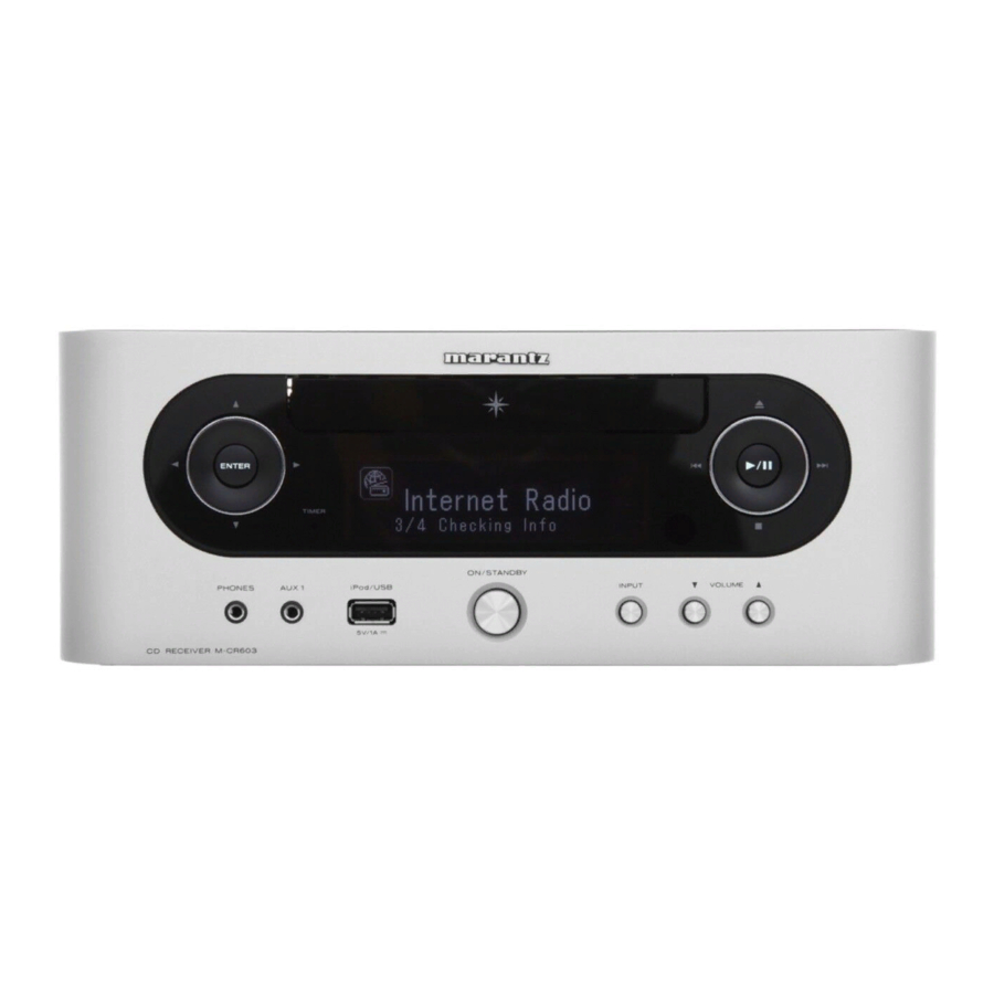
Marantz M-CR603 Service Manual
Hide thumbs
Also See for M-CR603:
- User manual (56 pages) ,
- Mode d'emploi (52 pages) ,
- Guía del usuario (52 pages)
Table of Contents
Advertisement
Service
Manual
• For purposes of improvement, specifications and design are subject to change without notice.
• Please use this service manual with referring to the operating instructions without fail.
• Some illustrations using in this service manual are slightly different from the actual set.
S0661-1V08DM/DG1304
M-CR603
M-CR603 /
N1SG/N1B
CD Receiver
/U1B
d
d
Ver. 8
Please refer to the
MODIFICATION NOTICE.
Advertisement
Table of Contents

Related Manuals for Marantz M-CR603


Summary of Contents for Marantz M-CR603
- Page 1 M-CR603 / Service N1SG/N1B /U1B Manual CD Receiver • For purposes of improvement, specifications and design are subject to change without notice. • Please use this service manual with referring to the operating instructions without fail. • Some illustrations using in this service manual are slightly different from the actual set.
- Page 2 MARANTZ Parts for your equipment are generally available to our National Marantz Subsidiary or Agent. ORDERING PARTS : Parts can be ordered either by mail or by Fax.. In both cases, the correct part number has to be specified.
- Page 3 SAFETY PRECAUTIONS The following check should be performed for the continued protection of the customer and service technician. LEAKAGE CURRENT CHECK Before returning the unit to the customer, make sure you make either (1) a leakage current check or (2) a line to chassis resistance check.
- Page 4 NOTE FOR SCHEMATIC DIAGRAM WARNING: Parts marked with this symbol z have critical characteristics. Use ONLY replacement parts recommended by the manufacture CAUTION: Before returning the unit to the customer, make sure you make either (1) a leakage current check or (2) a line to chassis resistance check. If the leakage current exceeds 0.5 milliamps, or if the resistance from chassis to either side of the power cord is less than 460 kohms, the unit is defective.
- Page 5 WARNING AND LASER SAFETY INSTRUCTIONS WARNING WAARSCHUWING All ICs and many other semi-conductors are Alle IC’s en vele andere halfgeleiders zijn susceptible to electrostatic discharges (ESD). gevoelig voor elektrostatische ontladingen Careless handling during repair can reduce (ESD). life drastically. Onzorgvuldig behandelen tijdens reparatie When repairing, make sure that you are kan de levensduur drastisch doen connected with the same potential as the...
- Page 6 INSTRUCTIONS FOR HANDLING SEMI-CONDUCTORS AND OPTICAL UNIT Electrostatic breakdown of the semi-conductors or optical pickup may occur due to a potential difference caused by electrostatic charge during unpacking or repair work. 1. Ground for Human Body Be sure to wear a grounding band (1 MΩ) that is properly grounded to remove any static electricity that may be charged on the body.
- Page 7 SPECIFICATIONS S/N ratio (mono) 65 dB n CDnplayer Sensitivity (S/N 30 dB) 9 dBµV (IHF) • Audio performance • AM tuner S/N ratio (1 kHz) 100 dB Range of receivable frequencies 522 to 1611 kHz Dynamic range (1 kHz) 100 dB S/N ratio 40 dB 0.01 %...
- Page 8 CAUTIONnINnSERVICING AboutnreplacenthenETHERNETnPCBnASS'Ynwithnannewnonen h • W hen you replace the ETHERNET PCB ASS'Y (8U-310055S), you need software updates. (1) Replace the ETHERNET PCB ASS'Y with the 8U-310055S (MAC Address was written). (2) A fter the M-CR603 built, DISC using firmware DM860 (Net (IMG)) to change the F Version. Refer to [ VERSIONn UPGRADEnPROCEDUREnOFnFIRMWAREn"1. How to update by disc" ] for the details of the Version up with disc. (3) M AC Address Label pasted to Bottom is pasted to Mac Address Label (GEN8341; MAC ADDRESS SUB ASSY ) of exchanged ETHERNET PCB ASS'Y and it substitutes it. (4) T he firmware is updated by DPMS. Refer to [ VERSIONnUPGRADEnPROCEDUREnOFnFIRMWAREn"2. How to update by DPMS" ] for the details of the Version up. InitializingnCDnRECEIVERn(FactorynReset) CD RECEIVER initialization should be performed when the μcom, peripheral parts of μcom, and Digital PCB. are replaced. 1. Turn off the power using ON/STANDBY button, unplug the power cord. 2. Plug the power cord into a power outlet while pressing VOLUME d and 2 button simultaneously. * Initialize. Note: • A ll user settings will be lost and this factory setting will be recovered when this initialization mode. So make sure to memorize your setting for restoring after the initialization. VOLUMEd Servicentools...
- Page 9 DISASSEMBLY • Disassemble in order of the arrow of the figure of following flow. • In the case of the re-assembling, assemble it in order of the reverse of the following flow. • In the case of the re-assembling, observe "attention of assembling" it. • I f wire bundles are untied or moved to perform adjustment or parts replacement etc., be sure to rearrange them neatly as they were originally bundled or placed afterward. Otherwise, incorrect arrangement can be a cause of noise generation. CAUTION: T hrough great care is taken when manufacturing parts from sheet metal, there may in some rare cases be burrs on the edges of top cover which could cause injury if fingers are moved across them. Use gloves to protect your hands. SIDE PANEL TOP COVER TOP PANEL and FRONT PANEL ASSY Refer to "DISASSEMBLY 1. TOP PANEL and FRONT PANEL ASSY" and "EXPLODED VIEW" TOP COVER (Ref. No. of EXPLODED VIEW : M4) FRONT PANEL ASSY (Ref. No. of EXPLODED VIEW : C1)
- Page 10 About the photos used for descriptions in the DISASSEMBLY" section. • T he direction from which the photographs used herein were photographed is indicated at "Direction of photograph: ***" at the left of the respective photographs. • Refer to the table below for a description of the direction in which the photos were taken. • Photographs for which no direction is indicated were taken from above the product. The viewpoint of each photograph Direction of photograph: B (Photography direction) Front side [View from above] Direction of photograph: D Direction of photograph: C Direction of photograph: A...
- Page 11 1. TOP COVER and FRONT PANEL ASSY Proceeding : SIDE PANEL TOP COVER and FRONT PNAEL ASSY → (1) Remove the screws. View from bottom Direction of photograph: A Direction of Direction of photograph: C photograph: D...
- Page 12 (2) Cut the wire clamp band, then disconnect the connector wires and the FFC Cable. Direction of photograph: D FFC Cable CN44 (3) Remove the TOP COVER and FRONT PANEL ASSY. TOP COVER TOP COVER FRONT PANEL ASSY (4) Disconnect the connector wire. CN0101...
- Page 13 (4) Remove the TOP COVER. TOP COVER Please remove TOP COVER while lifting the hook. Please refer to "EXPLODED VIEW" for the disassembly method of each PCB included in FRONT PANEL ASSY.
- Page 14 2. CD MECHA ASSY Proceeding : SIDE PANEL → TOP COVER and FRONT PNAEL ASSY CD MECHA ASSY → (1) Remove the screws. (2) Laser short-circuit in Pick-up of CD MECHANISM ASS'Y, then disconnect the connector wires and FFC cable. Be sure to wear a grounding band. Soldering place FFC Cable Direction of photograph: A (3) Disconnect the connector wires. Direction of photograph: C Please refer to "EXPLODED VIEW" for the disassembly method of each PCB included in ETHERNET PCB ASSY and DAB PCB ASSY, TUNER MODULE.
- Page 15 3. MAIN PCB ASSY Proceeding : SIDE PANEL → TOP COVER and FRONT PNAEL ASSY CD MECHA ASSY → → MAIN PCB ASSY (1) Remove the SHEET COVER. Direction of photograph: A (2) Remove the screws. Direction of photograph: A (3) Remove the screws View from bottom...
- Page 16 (4) Remove the SUPPORT MECHA. SUPPORT MECHA (5) Remove the screws, then disconnect the FFC cable and the connector wire. CN45 CN43 CN61...
- Page 17 4. SMPS PCB ASSY Proceeding : SIDE PANEL → TOP COVER and FRONT PNAEL ASSY CD MECHA ASSY → SMPC PCB ASSY → (1) Remove the screws. View from bottom (2) Cut the wire clamp band, then disconnect the connector wires. Remove the screws. CN45 CN43 Direction of photograph: D CN61...
- Page 18 (3) Remove the screws. Direction of photograph: B (4) Remove the screws. Direction of photograph: A...
- Page 19 NOTE HANDLING AND REPLACEMENT OF THE LASER PICK-UP 1. Protection of the LD Short a part of the LD circuit by soldering. After connection to a circuit, remove the short solder. 2. Precautions when handling the laser CD mechanism • Handle the laser pick-up so that it is not exposed to dust. •...
-
Page 20: Table Of Contents
SPECIAL MODE Special mode setting Plug AC cord into power outlet while pressing buttons A and B. Each button continue to press until the lit of ENTER and 1 / 3 . Mode Button A Button B Contents Initialization mode VOLUME UP STOP Initializing. -
Page 21: Initialization Mode (Factory Reset)
1. Initialization mode (Factory Reset) Backup data initialization is carried out. Refer to Initialization Items. After initialization, move on to normal mode. CAUTION Version information (such as rewriting failed log) Clear. Clear the history of protection. "Initial value of laser current"and"The accumulated laser on time"not cleared. Power failure flag is not cleared. -
Page 22: Initialization Mode (User Reset)
2. Initialization mode (User Reset) Backup data initialization is carried out. Refer to Initialization Items. After initialization, move on to normal mode. CAUTION The difference is the following two points. Version information (such as rewriting failed log) not cleared. History of protection not cleared. Startup display "Initialized"... - Page 23 Pressing the ENTER button will be displayed below. Press Cursor 1 The version of the system-uP. Press Cursor f The version of the boot loader(system-uP). Press Cursor f The version of the display-uP. Press Cursor f The version of the boot loader(network-uP). Press Cursor f The version of the image(network-uP).
-
Page 24: Cd Test Mode
4. CD test mode Startup display "CD Test Mode" displayed for 5 seconds. CDCD TEST MODE display To exit this mode, unplug the power cord. 4.1. Before starting the test Open the tray and disc. Even if the disk is, the tray must let OPEN → CLOSE. Press the 2 button to return to "0 CD TEST MODE". - Page 25 r TRACKING ON Press 1 / 3 button t SUB CODE readout (playback sound output) The BER (Block Error Rate) generated in 1second's time is displayed of the display. Press 8 button Press 9 button Press 8 button Press 9 button Inner (IN), Ataru Amane (MID), outer (OUT) to play go to three places, make the error count.
- Page 26 (Caution) If you have not completed the adjustment, the value is not correct. 4.5. All servo on and auto adjustment. When Volume d button is pressed for over 1 second while the M-CR603 is in the CD TEST MODE, the laser turns on and the laser current is measured.
- Page 27 4.6. Accumulated laser on time display When the Volume f button is pressed while the M-CR603 is in the "CD TEST MODE"displayed, the accumulated laser on time is displayed. The laser drive times are added and the result is displayed.
-
Page 28: Heat Run Mode
5.2. Heat run Short mode Playing last track on disc. After disc playback has finished, then tray open and close. And playback again. The heat run repetition no. is incremented (increased by 1) when the tray is opened. Repeat this operation. [H.R. -
Page 29: Product Mode
6. Product Mode 1 Startup display "Product Mode1" displayed for 5 seconds. Tested during production to perform the following settings automatically. Tuner Preset To exit this mode, unplug the power cord. 7. Product Mode 2 Startup display "Product Mode2" displayed for 5 seconds. Tested during production to perform the following settings automatically. - Page 30 Potential difference across the terminal detects that the speaker was more than DC9V DC protect 1 Overvoltage of +B/-B DC protect 2 Short of '+B/-B Over current Over-current detection digital amplifier SubWoofer DC protect Over voltage Supply voltage is detected beyond the provisions Protection history is reset.
-
Page 31: Hidden Serial Number Mode
9. Hidden serial number mode Serial number writing mode. This mode is for production only, not described in detail. 10. Update mode (by disc) Firmware update disc by. When you replace the ETHERNET PCB ASS'Y (8U-310055S), you need software updates. Refer to [ VERSION UPGRADE PROCEDURE OF FIRMWARE "1. -
Page 32: Dpms Compulsion Update Mode
Error code table Error Code Details of Error code Tray Open/Close failure No Disc Disc error(TOC not read ) No update file Update file read error Update file check sum error Erase failure Write failure Verify incorrect Update file check sum error Erase failure Write failure Verify incorrect... - Page 33 • Firm error codes at the main microprocessor rewritten. (Check main microprocessor ) Error Details of Error code Coping strategies Code Firm Info response acquisition TimeOut(Main rewrite Turn off and on the power. Updating starts automatically. Firmware recived failure(TimeOut)) Firm Info response acquisition recived error(Main rewrite Turn off and on the power.
-
Page 34: Compulsion Update Mode (By Rs232C)
• DM8x0 system Firm error codes when rewriting. (Check ETHERNET unit) Error Details of Error code Coping strategies Code Check the network connection. Carry out the update in an environment that has little Net not connected network load. Check the network connection. Carry out the update in an environment that has little Net Connection TimeOut can not get status network load. - Page 35 ABOUT REPLACE THE MICROPROCESSOR WITH A NEW ONE When replaced of the U-PRO (Microprocessor) or the Flash ROM, confirm contents of the following. After PWB Name Ref. No. Description Remark replaced DISPLAY IC81 R5F64169DFD MAIN IC11 R5F64169DFD After replaced A : Mask ROM (With software). No need write-in of software to the microprocessor. B : Flash ROM (With software).
- Page 36 (3) Please put CD-R on Tray, and press 5 button. (4) After loading CD-R, version number of firmware will be indicated. xxxxxx : Version number (5) If there is no any firmware of updating, [xxxxxx="None"] will be indicated. Please confirm version of each firmware by Cursor d / f buttons. (6) Press "Enter"...
- Page 37 1.3. Trouble Shooting If you find the following Error codes, please solve root cause of malfunction. (1) If updating is failed, the following ERROR indication is displayed. First line (Error number): "Updating fail: YY, n/N"YY: Error number Second line (Time on error): "xx min yy%" Third line (name of firmware) Error code table Error Code...
- Page 38 Even with a broadband connection to the Internet, approximately about 1 hour is required for the updating procedure to be completed. Once updating starts, normal operations on the M-CR603 cannot be performed until updating is completed. Also, setting items of the image adjustment may be initialized.
- Page 39 TROUBLE SHOOTING 1. OLED dosen't light Check Power Supply Voltages for System µ-com. Check Soldering. MAIN B'D • [IC12] on MAIN B'D • +6V_CPU, [CN43] : 4pin • [CN43] : 4pin • +3.3V_CPU, [IC12] : 3pin • SMPS B'D Check Reset signal for System µ-com. MAIN B'D Check Soldering.
- Page 40 2. No Sound,Noise generated 2.1. COMMON Check Power Supply Voltages for CODEC. Check Soldering. MAIN B'D • [IC13] : 3pin +5V • [IC41] : 1,20,33,43,50pin VDD +5V • [CN45] : 10pin +3.3VD • [IC41] : 18pin VDD +3.3V O.K.? Check Power Supply Voltages for PWM CONTROLLER. Check Soldering.
- Page 41 Check control signal for PWM CONTROLLER. MAIN B'D Check Soldering. • [IC51] : 24,25pin • [IC11] : 94,92pin 5508_SDA, 5508_SCL 5508_SDA, 5508_SCL on MAIN B'D • [IC51] : 13,14pin • [IC51] : 13,14pin PDN,MUTE on MAIN B'D PDN,MUTE "H" level O.K.? 2.2.
- Page 42 Check PWM Audio Data output from PWM CONTROLLER. MAIN B'D SPEAKER A Check Soldering. • [IC51] : 46,47,42,43pin • [IC51] on MAIN B'D SPEAKER B • [IC51] : 44,45,40,41pin Check PWM Audio Data output for PWM CONTROLLER. MAIN B'D SPEAKER A Check Soldering.
- Page 43 2.3 . AM/FM TUNER-in Check Soldering. Check Power Supply Voltages for AM/FM TUNER. • [CN45] : 2pin +12V on MAIN B'D MAIN B'D • SMPS B'D • [CN31] : 4pin +9V Check Parts • [CN45] : 2pin +12V • [IC26] Check Analog Audio Data output from TUNER PACK.
- Page 44 2.6 . AUX2/AUX3 Check Analog Audio Signal from AUX2/AUX3. Check Soldering. MAIN B'D • [JK63] on MAIN B'D • [AUX2], [AUX3] input • [C422], [C423] on MAIN B'D • [IC41] : 55,56pin AUX2_L_IN, AUX2_R_IN • [C420], [C421] on MAIN B'D •...
- Page 45 2.8 . USB/ETHERNET Check Soldering. • [N0103] : 1,2pin +6V on ETHERNET B'D Check Power Supply Voltages for ETHERNETNET B'D. • [N0103] : 5,6pin +15V on ETHERNET B'D ETHERNET B'D • [BN62] : 1,2pin +6V on MAIN B'D • [N0103] : 1,2pin +6V •...
- Page 46 MEASURING METHOD AND WAVEFORMS To check the waveforms, the GND (-) probe of the oscilloscope to specified reference voltage. (Except for inner SW, TRVSW) NOTES Measuring Disc: CD/TCD-784 CD-R/TCD-R082W CD-RW/TCD-W082W (It is better to use wires for extending between the probe and test points.) •...
- Page 47 Foil side Detail C Symbol Symbol Reference voltage RFEQO Ⓐ VC : q ~ i Ⓑ C900 - DGND : Q3 ~ Q5 Ⓒ CN26(4) GND_DRV : o ~ Q2 FOC1 TRO1 FMO1 DMO1 CN26(3) OPSW CN26(5) CLSW CN26(2) LOAD+ CN26(1) LOAD- R407...
- Page 48 2. WAVEFORMS 1. DISC PLAY RF WAVEFORM (EYE-PATTERN) 2. DISC DETECTION CD(TCD784) DETECTION CD(TCD784) PLAY 1V/div w RFO 500mV/div e FEI 1V/div r FOO q RFEQO 1V/div t TEI 1V/div y TRO 500mV/div u FMO 1V/div i DMO 3. TOC READ 4.
- Page 49 5. CD Playback Q3 L RCK Q4 S CLK Q5 S DATA STANDARD GND WF12 (9) 6. LOADER OPEN-CLOSE o OPSW Q0 F CLSW Q2 L OAD- Q1 L OAD+ OPEN CLOSE STANDARD GND...
- Page 50 Personal notes:...
- Page 51 BLOCK DIAGRAM...
- Page 52 POWER DIAGRAM...
- Page 53 LEVEL DIAGRAM AK4683 TAS5508 TUNER AUDIO CODEC PWM CONTROLLER TAS5142DKD PACK DIGITAL AMP SP L OUT CD UNIT TAS5142DKD DIGITAL AMP SP R OUT TC94A92FG AUX1 MUTE PHONES AUX2 M-X PORT MUTE SUBWOOFER OUT MUTE AUX OUT SP OUT Impedance 8 ohm +20dB 17.88V (18.8dB) X 2ch SP A o VOL MAX : +10dB(6V)
- Page 54 WIRING DIAGRAM...
- Page 55 PRINTED WIRING BOARDS MAIN PCB (COMPONENT SIDE) 鉛フリー半田 半田付けには、鉛フリー半田 (Sn-Ag-Cu) を使用してください。 Lead-free Solder When soldering, use the Lead-free Solder (Sn-Ag-Cu).
- Page 56 MAIN PCB (FOIL SIDE) 鉛フリー半田 半田付けには、鉛フリー半田 (Sn-Ag-Cu) を使用してください。 Lead-free Solder When soldering, use the Lead-free Solder (Sn-Ag-Cu).
- Page 57 DISPLAY PCB (COMPONENT SIDE) DAB PCB (COMPONENT SIDE) DISPLAY PCB (FOIL SIDE) DAB PCB (FOIL SIDE) 鉛フリー半田 半田付けには、鉛フリー半田 (Sn-Ag-Cu) を使用してください。 Lead-free Solder When soldering, use the Lead-free Solder (Sn-Ag-Cu).
- Page 58 ETHERNET PCB (COMPONENT SIDE) ETHERNET PCB (FOIL SIDE) CUP12318Z ADJ1 ADJ2 C4216 C4211 U105 R4218 R4211 R4214 U0104 R4212 C0130 C0133 C0134 R4220 C4206 C4204 C4209 R4219 R4213 R4221 R0124 R4222 R0126 N4201 C3937 R4215 C0129 C3915 Q0104 C0140 C3914 C0128 R4216 C4213...
- Page 59 TUNER BLOCK SHEET 001 FM/AM TUNER KSE_TUNER +9V_T KDS160 D302 CN31 +12V_A R128 R126 PORT_SEL IC26 KIA78R090F R125 R127 TUNED L_OUT L301 STEREO R_OUT C353 GND_A 0.1uF L302 RDS_CLK RDS_DATA OPEN GND_D1 R314 TUNED R315 STEREO R316 TU_SDA R317 TU_SCL R318 RDS_CLK R319...
- Page 60 D609 SW_DOWN R600 MX_RC-5 1SS355T D501 1SS355T D503 1SS355T +12V_A GND_A D502 1SS355T D504 1SS355T C539 SW OUT PARTS Q608 * Only M-CR603 +12V_A C489 0.1u C490 0.1u 0.1u KTC4075GR R619 C540 R601 GND_A +5V_STBY GND_A Q609 0.01u DETECT KTC4075GR...
- Page 61 R200 R285 R982 R289 R997 R288 R282 R287 MODEL GND_D1 C603 1000P C606 1000P M-CR603 OPEN 150 OPEN 180 OPEN 270 OPEN 1K CN24 +15V_USB/Wi-Fi(1.5A) RESET. RESET RCD-N7 OPEN OPEN OPEN OPEN OPEN OPEN OPEN OPEN OPEN +15V_USB/Wi-Fi(1.5A) +3.3V_CPU TXD_CO...
- Page 62 TO MAIN CPU BLOCK SHEET 003 CD DSP BLOCK SHEET 004 R211 FCO1 TRO1 LD_CHK +VREF FCS- +3.3V_D3 OPEN R206 +1.5V_D2 TRK- TRO2 FCO2 0.047u C220 TRK+ 0.047u C219 FCS+ LD PD OPEN C218 R231 SBSY LD VR R204 1SS355T D201 LD LD +3.3V_D3...
- Page 63 PWM/AMP BLOCK SHEET 005 PWM CONTROLLER PARTS +3.3V_D1 +3.3V_5508 AMP PARTS R681 +32V OPEN +12V_5142 5142_OTW R543 OPEN R540 R544 OPEN LOW ESR 5142_SD 10/63V RCD-N7 Not Used C719 (RFO) VALID R101 OPEN C523 L705 L706 C501 L501 VRA_PLL VR_PWM 0.1uF R539 0.1uF...
- Page 64 R863 R864 VDDIO KEY2. R808 BUSY_CO P102/AN2 KEY1. P67/TXD1 R807 SCLK_CO P101/AN1 P65/CLK1 R991 R993 P70/TXD2 * Only M-CR603(N VERSION) AVCC Bracket GND AVSS P97/RXD4 R806 R838 OPEN RXD_CO GND_OELD3 GND_OELD2 GND_OELD1 P100/AN0 P66/RXD1 * F VERSION is OPEN. VLSS...
- Page 65 SCHEMATIC DIAGRAMS (7/9) POWER + POWER -...
- Page 66 +15V_U/W USB_P.CONT DC_PROTECT2 VBUS MAIN BLOCK Sheet TO DM860 +5V_D1 L0101 10uH CMI-SSP12L80F U0103 E_POWER_CONT SI-8005Q-TL VBUS_MONI DGND COMP DGND Q0101 FDC608PZ DGND USBVBUS FAULT_FLAG1 +5V_D1 U0101 +15V_U/W N0103 microSMD175F D0103 +5V_D1 8P-PH R0103 OPEN Q0105 R0109 KDS160 R0104 OPEN OPEN DTC123EKA U105...
- Page 67 S H E L L R3900 OPEN Debug_RX Debug_TX 3.3V CORE 0.8W 0.67A SDRAM N3900 DM_D0 I/O 0.7W 0.21A DM_D0 P18 OPEN DM_D1 DM_D1 P19 DM_D2 DM_D2 P20 DM_D3 DM_D3 R18 DM_D4 J T A G DM_D4 R19 USBD- NET3.3V DGND DGND NET3.3V...
- Page 68 EXPLODED VIEW WARNING: Parts marked with this symbol have critical characteristics. Use ONLY replacement parts recommended by the manufacturer.
- Page 69 Ref. No. Part No. Part Name Remarks Q'ty M-CR603/NISG DISPLAY PCB ASS'Y COP12317B M-CR603/NISG MAIN PCB ASS'Y COP12316B M-CR603/NISG SMPS PCB ASS'Y COP12319B...
- Page 70 Ref. No. Part No. Part Name Remarks Q'ty SHEET, COVER CHS1A154 SHEET CMX1A180Z SCREWS SCREW , SPECIAL N1SG CHD1A063 SCREW , SPECIAL N1B,U1B CHD1A063ZR SCREW CTB26+8JFZR SCREW CTW3+8JR SCREW CTB3+10JR SCREW CTB3+8JFZR SCREW CTW3+12JR SCREW CTB3+10JFZR SCREW CTB3+8JR SCREW CTB3+6FFZR SCREW CTB3+6JR SCREW...
- Page 71 BAG , POLY CPB1A008Z 5 943611000190S CORD , POWER EUR(H03VVH2-F 2X0.75MM NM) N1SG,N1B CJA2B108ZV 5 943611000230S POWER CORD UL CJA2A107ZV CJA2A107ZV 6 307010079001M REMOCON TRANSMITER ASS'Y (M-CR603) CARTMCR603 7 943535001070D BAG , POLY(ENGLISH/FRANCH) CPB1061W 8 541110506005M MANUAL, INSTRUCTION(E2) N1SG,N1B CQX1A1561Z...
- Page 72 SEMICONDUCTORS Only major semiconductors are shown, general semiconductors etc. are omitted to list. The semiconductor which described a detailed drawing in a schematic diagram are omitted to list. 1. IC's R5F64169DFD (MAIN : IC11, DISPLAY : IC81) (Note 1) IIO0_0 / IIO1_0 / D8 / P1_0 P4_4 / CS3 / A20 / CTS6 / RTS6 / SS6 AN0_7 / D7 / P0_7 P4_5 / CS2 / A21 / CLK6...
- Page 73 5F64169DFD (MAIN : IC11) Terminal Function Network Pin No Pin Name Port Name I/O STBY Note STBY P96/(TXD4) UART_MOSI Transfer Data for Display ucom at Updating (P95)/CLK4 LED_CONT1 LED Control1 P94/(CTS4) LED_CONT2 LED Control2 P93/(CTS3) OLED_CPU_POWER PD Power Control for Display ucom P92/TXD3 EL_MOSI Display Data for Display ucom P91/RXD3 EL_MISO Display Data from Display ucom...
- Page 74 Network Pin No Pin Name Port Name I/O STBY Note STBY P53/BCLK P52/RD CHECK-4 P51/(WR1)/BC1 SRAMSTB Control for TC94A92FG SRAMSTB P50/(WR0)/WR/CE CE_M Rewrite boot program start : H input set P127 Chip Enable for CD DSP P126 BUCK BUS Clock for CD DSP P125 P47/CS0/(A23) BUS3...
- Page 75 Network Pin No Pin Name Port Name I/O STBY Note STBY P152/RXD7 HVBUS_CTL1 USB1 VBUS Control P151/(CLK7) FAULT_FLAG1 USB1 VBUS Current Limit Signal P150/TXD7 /B1/B2 USB BUS Switch Control (RCD-N7) P107/(AN7)/(KI3) HVBUS_CTL2 USB2 VBUS Control (RCD-N7) P106/AN6/KI2 KEY3 Key Input3 P105/AN5/KI1 KEY2 Key Input2 P104/AN4/KI0 KEY1 Key Input1...
- Page 76 R5F64169DFD (DISPLAY : IC81) Terminal Function Pin No Port Name Symbol Pull-U/D Note P96/(TXD4) PD(OPEN) NC (P95)/CLK4 P94/(CTS4) P93/(CTS3) P92/TXD3 P91/RXD3 P90/(CLK3) (P146)/INT8 P145/INT7 P144/INT6 P143 VDC0 VDC0 Smoothing capacitor connection terminal P141(INPUT ONLY) VDC1 VDC1 Smoothing capacitor connection terminal Emulator communication pin Single-chip / Micro-processor mode switching CNVSS(INPUT ONLY) CNVSS (Normal single-chip : L, Rewrite boot program start : H input set) P87/(XCIN)
- Page 77 Pin No Port Name Symbol Pull-U/D Note P50/(WR0)/WR/CE CE_M Rewrite boot program start : H input set P127 RES# Reset, Active "L" for OLED P126 Chip select : "L" for OLED (I/F communicate possible) P125 RES# Reset, Active : "L" for OLED P47/CS0/(A23) R/W#,WR# Write (This pin stays "L"(low) in Serial Interface Mode) for OLED...
- Page 78 Pin No Port Name Symbol Pull-U/D Note P107/(AN7)/(KI3) P106/AN6/KI2 P105/AN5/KI1 P104/AN4/KI0 P103/AN3 P102/AN2 P101/(AN1) AVSS AVSS P100/AN0 Not use VREF VREF AVCC AVCC (P97)/RXD4...
- Page 79 TC94A92FG (MAIN : IC21) VDD3 CDMoN3 BUS0 Pio14/CDMoN2 BUS1 Pio13/CDMoN1 BUS2 Pio12/CDMoN0/FGiN BUS3 Pio11 BUCK Pio10 /CCE Pio9 TC94A92FG Pio8 /RST VDD1-3 (Top View) TEST VDD1-1 FMoS VSS-1 /SRAMSTB VSS-3 VDDM1 TMAX AVDD3 LPFN LPFo RFRP PVREF RFZi VCoF FSMoNiT 2009-05-27...
- Page 80 TC94A92FG Block Diagram TC94A92FG Block Diagram SRAM SRAM 512kbit 512kbit MCU I/F SLCo Resume (4kw*128bit) (4kw*128bit) DSP-VCO TMAX PVREF PVREF SRAM I/F RVDD3 RVSS3 Synchronous Subcode RF Ripple guarantee EFM RFRPi DET.(RFRP) decoder decoder round & limit round & limit Instruction Auto Gain Decoder Pio7 AGCi...
- Page 81 TC94A92FG 1. Pin Descriptions TC94A92FG Terminal Function 1.1 Pin Descriptions Symbol Description Remarks Default DSP VCO - EFM and PLCK Phase difference VCoi signal output pin. 3 state output 3AI/F (DSP VCO control voltage inputr pin.) CD-DSP-Power supply for 3.3V RF RVDD3 amplifier core and PLL circuit Connect capacitor according with se SLCo...
- Page 82 TC94A92FG Symbol Description Remarks Default Focus Error signal / Sub beam add signal FSMoNiT 3AI/F output pin(monitor pin/GND) RFZi RF ripple zero-cross signal Input pin 3AI/F RFRP RF ripple signal output pin. 3AI/F Bulit-in serises R=500Ω. Connect to VRo by Tracking error signal output pin.
- Page 83 TC94A92FG Symbol Description Remarks Default DVSS3R Grounding pin for 3.3V Muiti-Bit DAC circuit R channel audio output pin of Audio DAC. 3AI/F DVDD3R Power supply pin for 3.3V Audio DAC circuit. DVDD3L Power supply pin for 3.3V Audio DAC circuit. L channel audio output pin of Audio DAC 3AI/F DVSS3L...
- Page 84 TC94A92FG Symbol Description Remarks Default VDD3 Power Supply pin for 3.3V Digital circuit CMOS Port Schmitt input BUS0 Microprocessor I/F data input/output pin 0 3I/F Refer to [1.2 Pin Assinment Table] CMOS Port Schmitt input BUS1 Microprocessor I/F data input/output pin 1 3I/F Refer to [1.2 Pin Assinment Table] CMOS Port...
- Page 85 The IP4001 is a monolithic integrated circuit, and 5-CH MOTOR DRIVE IC suitable for 5-ch motor driver which drives focus actuator, tracking actuator, sled motor, spindle motor and Tray motor of CDP & V-CD system. PIN CONNECTIONS IP4001CRLTF (MAIN : IC31) 28SSOP H/S (FIN) PGND2 DO4- DO4+ IN4A VCC2...
- Page 86 ■ ピン配置 AK4683 (MAIN : IC41) 64 63 62 61 60 59 58 57 56 55 54 53 52 51 50 49 PVDD RISEL ROPIN LOPIN LISEL AVSS2 AVDD2 VCOM AK4683EQ ROUT2 VOUT Top View LOUT2 CDTO ROUT2 LRCKB BICKB LOUT2 SDTOB MUTET OLRCKA ILRCKA...
- Page 87 [AK4683] ピン/機能 AK4683 Pin Discriptions Pin Name Function PVDD PLL Power supply Pin, 4.5V∼5.5V Receiver Channel 0 Pin (Internal biased pin. Internally biased at PVDD/2) Control Mode Select Pin. “L”: 4-wire Serial, “H”: I C Bus Receiver Channel 1 Pin Receiver Channel 2 Pin Receiver Channel 3 Pin Interrupt Pin VOUT...
- Page 88 [AK4683] Pin Name Function LOUT2 DAC2 Lch Positive Analog Output Pin DAC2 Rch Positive Analog Output Pin ROUT2 DAC1 Lch Positive Analog Output Pin LOUT1 DAC1 Rch Positive Analog Output Pin ROUT1 DAC/ADC Common Voltage Output Pin VCOM 2.2μF capacitor should be connected to AVSS2 externally. AVDD2 DAC Power Supply Pin, 4.5V∼5.5V AVSS2...
- Page 89 The TAS5142 is available in two thermally enhanced packages: • 36-pin PSOP3 package (DKD) • 44-pin HTSSOP PowerPad™ package (DDV) Both package types contain a heat slug that is located on the top side of the device for convenient thermal coupling to the heatsink.
- Page 90 TAS5142 www.ti.com SLES126B – DECEMBER 2004 – REVISED MAY 2005 TAS5142 Block Diagram FUNCTIONAL BLOCK DIAGRAM Under- voltage Protection Internal Pullup VREG VREG Resistors to VREG Power Reset AGND Protection I/O Logic Temp. Sense RESET_AB Overload RESET_CD OC_ADJ sense Protection GVDD_D BST_D PVDD_D Gate PWM_D...
- Page 91 Physical Characteristics 2.1.1 Terminal Assignments PAG PACKAGE TAS5508 (MAIN : IC51) (TOP VIEW) 64 63 62 61 60 59 58 57 56 55 54 53 52 51 50 49 VRA_PLL VR_PWM PLL_FLT_RET PWM_P_4 PLL_FLTM PWM_M_4 PLL_FLTP PWM_P_3 AVSS PWM_M_3 AVSS PWM_P_2 VRD_PLL PWM_M_2 AVSS_PLL PWM_P_1...
- Page 92 TAS5508 8-Channel Digital Audio PWM Processor www.ti.com SLES091C – FEBRUARY 2004 – REVISED AUGUST 2005 TERMINAL TYPE TERMINATION DESCRIPTION TOLERANT NAME PWM_P_3 PWM 3 output (differential +) PWM_P_4 PWM 4 output (differential +) PWM_P_5 PWM 5 output (differential +) PWM_P_6 PWM 6 output (differential +) PWM_P_7 PWM 7 (lineout L) output (differential +)
- Page 93 TAS5508 8-Channel Digital Audio PWM Processor TAS5508 Block Diagram www.ti.com SLES091C – FEBRUARY 2004 – REVISED AUGUST 2005 Output Control 8 × 2 Crossbar Mixer 8 × 8 Crossbar Mixer AVSS AVDD DVSS DVDD DAP Control PWM Control VRD_PLL VRA_PLL VBGAP System Control AVDD_REF AVSS_PLL AVDD_PLL...
- Page 94 Pin Configuration and Functionality CS (Current Sense) The Current Sense pin senses the voltage developed Pin F Pin Configuration with PG-DIP-8-6 on the series resistor inserted in the source of the Package PG-DIP-8-6 integrated Depl. CoolMOS™. If CS reaches the internal ICE3B0365J (SMPS : IC91) SoftS (Soft Sta threshold of the Current Limit Comparator, the Driver...
- Page 95 Pin Confi Pin Configuration and Functionalit Package PG-DIP-8-6 Pin Configuration with PG-DIP-8-6 Pin C Package PG-DIP-7-1 ICE2B265 (SMPS : IC92) Symbol Function Symbol SoftS SoftS SoftS Soft-Start SoftS Feedback Isense Controller Current Sense Input, Isense CoolMOS™ Source Output Drain N.C. 650V /800V CoolMOS™...
- Page 96 Pin Configurati gate driver output IC supply voltage CS (Current Sensing) Pin Configuration and Functionality This pin is connected to the shunt resistor for the Common ground primary current sensing, externally, and the PWM signal generator for switch-off determination (together Pin Configuration REG (Regulation) Package PG-DIP-8...
- Page 97 W9825G6EH-6J (ETHERNET : U3902) DQ15 DQ14 DQ13 DQ12 DQ11 DQ10 LDQM UDQM A10/AP W9825G6EH-6J Block Diagram CLO CK BUFFER CO NTRO L SIG NAL G ENERATO R CO MMAND DECO DER CO LUMN DECODER COLUMN DECO DER CELL ARRAY CELL ARRAY BANK #1 BANK #0 MO DE REGIST ER SENSE AMPLIFIER...
- Page 98 W9825G6EH W9825G6EH-6J Pin Description 5. PIN DESCRIPTION PIN NUMBER PIN NAME FUNCTION DESCRIPTION Multiplexed pins for row and column address. 23−26, 22, Address A0−A12 29−36 Row address: A0−A12. Column address: A0−A8. Select bank to activate during row address latch time, or 20, 21 BS0, BS1 Bank Select bank to read/write during address latch time.
- Page 99 LAN8700 (HDMI : U4202) nINT/TX_ER/TXD4 TXD3 TXD2 CRS/PHYAD4 VDDIO USB3300 MDIO TXD1 LAN8700/LAN8700I Hi-Speed USB2 MII/RMII Ethernet PHY nRST TXD0 ULPI PHY 36 Pin QFN TX_EN TX_CLK 32 Pin QFN VDD33 RX_ER/RXD4 GND FLAG VDD_CORE RX_CLK/REGOFF SPEED100/PHYAD0 LAN8700 Block Diagram MODE0 HP Auto-MDIX Auto- 10M Tx MODE1 MODE Control Negotiation...
- Page 100 ±15kV ESD Protected MII/RMII Fast-Ethernet PHY with HP Auto-MDIX and SMSC flexPWR in a Small Footprint Datasheet LAN8700 Pin Description Table 2.1 LAN8700/LAN8700I 36-PIN QFN Pinout PIN NO. PIN NAME PIN NO. PIN NAME nINT/TX_ER/TXD4 RX_DV RX_CLK/REGOFF CRS/PHYAD4 RX_ER/RXD4 MDIO TXCLK nRST TXD0 TX_EN TXD1...
- Page 101 S020-MXS4003A-A 2. DISPLAY 15. IO インターフェイス IO Interfaces MXS4003A (DISPLAY : CN84) 端子番号 端子名 入出力 機能 Pin No. Pin Name Functions グランド ドライバー系陽極電源 Power supply for Anode Driver ドライバー系陰極電源 VCOMH Power supply for Cathode Driver アナロググランド VLSS Analog system ground データバス Data Bus データバス Data Bus データバス...
- Page 102 PARTS LIST OF P.C.B. UNIT zParts for which "nsp" is indicated on this table cannot be supplied. zThe parts listed below are for maintenance only, might differ from the parts used in the unit in appearances or dimensions. DISPLAY PCB ASSY Ref.
- Page 103 Ref. No. Part No. Part Name Remarks Q'ty C906 CAP , ELECT CCEA1CKS470T C907 CAP , CHIP (1608, 50V/0.1uF) CCUS1H104KC C908 CAP , ELECT CCEA1AKS101T C909 CAP , CHIP (1608, 50V/0.01uF) CCUS1H103KC C910 CAP , ELECT CCEA1CKS101T C911 CAP , CHIP (1608, 50V/0.01uF) CCUS1H103KC C912 CAP , ELECT...
- Page 104 Ref. No. Part No. Part Name Remarks Q'ty L932 RES , CHIP , 0 OHM, 5% , 1/8W , 2012 CRJ18AJ0R0T RC81 00MHW10004210 SENSOR , REMOCON CRVRPM6936V4 S901-915 90M-SP001210R SW , TACT CST1A012ZT COXCSTCE16M0V51 X802 943142011280S 16M Resonator...
- Page 105 MAIN PCB ASS'Y Ref. No. Part No. Part Name Remarks Q'ty SEMICONDUCTORS GROUP IC11 8R2431005400S MCU, IC (R32C/100, 144P6Q-A) CVIR5F64169DFD IC12 943231011000S I,C , REGULATOR(3.3V SMD Type) BVIBA33BC0FP IC13 943231011210S I.C , REGULATOR (SWITCH LOW DROP,5V,DPAK-5) CVIKIA78R050F IC18 90M-HC900160R I.C , REGULATOR(SOT-223) CVIKIA1117S15 IC21 943245006980S I.C , CD DSP (SERVO,AMPLIFIER,DSP,LQFP-80P)
- Page 106 Ref. No. Part No. Part Name Remarks Q'ty D231 DIODE , ZENER HVDMTZJ11BT D232 DIODE , ZENER HVDMTZJ20BT D233 DIODE , ZENER HVDMTZJ5.6BT D234 DIODE , ZENER HVDMTZJ7.5BT D235 DIODE , ZENER HVDMTZJ20BT D238,239 00D2760794900 DIODE , CHIP CVDKDS160RTKP D240 DIODE , ZENER HVDMTZJ16BT D241...
- Page 107 Ref. No. Part No. Part Name Remarks Q'ty C239 CAP , ELECT CCEA1AKS101T C240 CAP , CHIP (1608, 50V/0.1uF) CCUS1H104KC C241 CAP , CHIP (1608, 50V/47pF) CCUS1H470JA C242 CAP , CHIP (1608, 50V/0.1uF) CCUS1H104KC C243 CAP , ELECT CCEA1AKS470T C244 CAP , CHIP (1608, 50V/0.01uF) CCUS1H103KC C245...
- Page 108 Ref. No. Part No. Part Name Remarks Q'ty C407 CAP , CHIP (1608, 50V/0.01uF) CCUS1H103KC C409 CAP , CHIP (1608, 50V/0.1uF) CCUS1H104KC C410 CAP , ELECT CCEA1HH100T C411 CAP , ELECT CCEA1HH1R0T C412 CAP , CHIP (1608, 50V/0.1uF) CCUS1H104KC C413 CAP , ELECT CCEA1HH2R2T C414...
- Page 109 Ref. No. Part No. Part Name Remarks Q'ty C532 CAP , ELECT CCEA1EH470T C535,536 CAP , ELECT CCEA1HH100T C537,538 CAP , CHIP (1608, 50V/100pF) CCUS1H101JA C539-543 RES , CHIP(0 OHM , 5% , 1608) CRJ10DJ0R0T C550 RES , CHIP(0 OHM , 5% , 1608) CRJ10DJ0R0T C553-555 RES , CHIP(0 OHM , 5% , 1608)
- Page 110 Ref. No. Part No. Part Name Remarks Q'ty C719 00D2544692901 CE04W1J100MT(RFO) CCEA1HH100T C724-726 RES , CHIP(0 OHM , 5% , 1608) CRJ10DJ0R0T C731,732 00MDD95331300 CAP , CHIP CCUC1H331JA C733 CAP , METALIZED FILM(100V/0.47UF, 5%) CCME2A474JR08T C734,735 943132003110S CAP , CHIP (2012, 100V/0.1uF) CCUC2A104KC C736,737 943132003100S CAP , CHIP (2012, 100V/0.01uF)
- Page 111 Ref. No. Part No. Part Name Remarks Q'ty CN25 WAFER , STRAIGHT(DVD LOADER) CJP06GA19ZY CN26 WAFER , STRAIGHT CJP05GA19ZY CN31 WAFER(11P, ST 1.25MM) CJP11GA115ZY CN32 WAFER CJP11GA117ZY CN41 WAFER, STRSIGHT, 1MM, SMD CJP30GA193ZY CN42 WAFER , CARD CABLE (SMD, 1MM) CJP23GA193ZY CN43,44 LOCKING TYPE , STRAIGHT WAFER , 2MM...
- Page 112 ETHER NET PCB ASS'Y Ref. No. Part No. Part Name Remarks Q'ty SEMICONDUCTORS GROUP D0101 DIODE , ZENER (CHIP,7.5V) HVDUDZS7.5BSR D0102 DIODE , SCHOTTKY (40V,3A, DO-214AC) DELTA CVDSS34SR D0103-0105 DIODE , CHIP CVDKDS160RTKP Q0101 MOSFET (P-CH, 2.5V POWER TRENCH) CVTFDC608PZ Q0102 T.R , CHIP , SOT-23 HVTKRC102S...
- Page 113 IC, SDRAM (4M x 16Bit x 4Banks, 166Mhz, DRAM) CVIM12L2561616A6TG2K U4201 Pulse-Trans (HIGH SPEED LAN MAGNETICS) CVIS558-5999U7F U4202 I.C, ETHERNET PHY CVILAN8700CAEZGTR U4204 I.C , IPOD AUTHENTICATION CHIP FROM MARANTZ CVI236710076509S-DM X3900 X-tal (SMD, 24Mhz, FCX-05) COX24000I060SD Z4201,4202 BRACKET , PCB CMD1A569...
- Page 114 SMPS PCB ASS'Y Ref. No. Part No. Part Name Remarks Q'ty SEMICONDUCTORS GROUP IC90 90M-HC300960R I.C , REGULATOR(TO220IS-4) CVIKIA78D33PI IC91 943235003220S IC, CooLSET ICE3B0365J CVIICE3B0365J IC92 943235003200S IC , COOLSET CVIICE2B265 IC93 943235003210S I.C , PWM CONTROLLER(PG-DIP-8) CVIICE2QS01 IC94 00MHC3891899F I.C , VOL REGULATOR(18V, TO-220IS) CVIKIA7818API IC95,96 90M-HC300770R I.C , REGULATOR...
- Page 115 Ref. No. Part No. Part Name Remarks Q'ty C917 CAP , CERAMIC CCKT3A222KBL C918 943132002470S CHIP, CAP 0.1UF/50V/2012 CCUC1H104KC C919 CAP , CHIP CCUC1H103KC C921 943132002470S CHIP, CAP 0.1UF/50V/2012 CCUC1H104KC C922 943134003030S CAP , ELECT(KRM, 100V/1UF, 105C, 5X11) CCEA2AH1R0TS C923 943132002470S CHIP, CAP 0.1UF/50V/2012 CCUC1H104KC C924...
- Page 116 LF91,92 943149003340S LINE FILTER(10MH) CLZ9Z086Z z PC91-95 90M-HW100710R I.C , PHOTO COUPLER HVIPC17L1CB z TF91 943102011250S TRANS , SWITCHING (EE1625, M-CR603) CLT9Z064ZE z TF92 943102011260S TRANS , SWITCHING (EE2525, M-CR603) CLT9Z065ZE z TF93 943102011270S TRANS , SWITCHING (EER4042, M-CR603)
Need help?
Do you have a question about the M-CR603 and is the answer not in the manual?
Questions and answers