Table of Contents
Advertisement
Quick Links
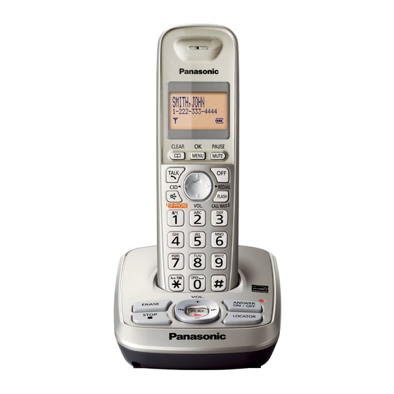
Caller ID Compatible
KX-TGA421N
(Handset)
(Charger Unit)
Configuration for each model
Model No
Base Unit
Handset
KX-TG4221
1 (TG4221) 1 (TGA421)
KX-TG4222
1 (TG4221) 2 (TGA421)
KX-TG4223
1 (TG4221) 3 (TGA421)
KX-TG313SK 1 (TG4221) 3 (TGA421)
KX-TG4224
1 (TG4221) 4 (TGA421)
KX-TG4225
1 (TG4221) 5 (TGA421)
Information for optional accessories
You can expand your phone system by registering optional
handsets (KX-TGA421) to a single
base unit.
Optional handsets and the supplied handset are different model
so that some functions may not be available.
Refer to each Operating Instruction for details.
KX-TG4221N
(Base Unit)
Charger Unit Expandable
Up to 6
1
Up to 6
2
Up to 6
2
Up to 6
3
Up to 6
4
Up to 6
Telephone Equipment
KX-TG4221N
Model No.
KX-TG4222N
KX-TG4223N
KX-TG313SK
KX-TG4224N
KX-TG4225N
KX-TGA421N
Digital Cordless Answering System
N: Champagne Gold Version
(for U.S.A.)
© Panasonic System Networks Co., Ltd. 2013
Unauthorized copying and distribution is a violation
of law.
ORDER NO. KM41301650CE
F13
Advertisement
Table of Contents

Related Manuals for Panasonic KX-TG4221N


Summary of Contents for Panasonic KX-TG4221N
- Page 1 Optional handsets and the supplied handset are different model so that some functions may not be available. Refer to each Operating Instruction for details. © Panasonic System Networks Co., Ltd. 2013 Unauthorized copying and distribution is a violation of law.
- Page 2 KX-TG4221N/KX-TG4222N/KX-TG4223N/KX-TG313SK/KX-TG4224N/KX-TG4225N/KX-TGA421N WARNING This service information is designed for experienced repair technicians only and is not designed for use by the general public. It does not contain warnings or cautions to advise non-technical individuals of potential dangers in attempting to service a product. Products powered by electricity should be serviced or repaired only by experienced professional technicians.
-
Page 3: Table Of Contents
16.2. Cabinet and Electrical Parts (Handset)------------- 76 10.1.11. Check Caller ID --------------------------------------42 16.3. Cabinet and Electrical Parts (Charger Unit) ------- 77 11 Disassembly and Assembly Instructions ---------------43 16.4. Accessories and Packing Materials ----------------- 78 11.1. Disassembly Instructions -------------------------------43 16.4.1. KX-TG4221N ----------------------------------------- 78... - Page 4 KX-TG4221N/KX-TG4222N/KX-TG4223N/KX-TG313SK/KX-TG4224N/KX-TG4225N/KX-TGA421N 16.4.2. KX-TG4222N ----------------------------------------- 79 16.4.3. KX-TG4223N/ KX-TG313SK --------------------- 80 16.4.4. KX-TG4224N ----------------------------------------- 81 16.4.5. KX-TG4225N ----------------------------------------- 82 16.4.6. KX-TGA421N----------------------------------------- 83 16.5. Replacement Parts List --------------------------------- 84 16.5.1. Base Unit ---------------------------------------------- 84 16.5.2. Handset ------------------------------------------------ 85 16.5.3. Charger Unit ------------------------------------------ 86 16.5.4.
-
Page 5: Safety Precautions
KX-TG4221N/KX-TG4222N/KX-TG4223N/KX-TG313SK/KX-TG4224N/KX-TG4225N/KX-TGA421N 1 Safety Precautions 1.1. For Service Technicians • Repair service shall be provided in accordance with repair technology information such as service manual so as to prevent fires, injury or electric shock, which can be caused by improper repair work. -
Page 6: Suggested Pbf Solder
KX-TG4221N/KX-TG4222N/KX-TG4223N/KX-TG313SK/KX-TG4224N/KX-TG4225N/KX-TGA421N Component Component Remove all of the excess solder Solder (Slice View) 2.2.1. Suggested PbF Solder There are several types of PbF solder available commercially. While this product is manufactured using Tin, Silver, and Copper (Sn+Ag+Cu), you can also use Tin and Copper (Sn+Cu), or Tin, Zinc, and Bismuth (Sn+Zn+Bi). Please check the manufacturer's specific instructions for the melting points of their products and any precautions for using their product with other materials. -
Page 7: Specifications
KX-TG4221N/KX-TG4222N/KX-TG4223N/KX-TG313SK/KX-TG4224N/KX-TG4225N/KX-TGA421N 3 Specifications N Standard: Bit rate: DECT 6.0 (Digital Enhanced Cordless 1,152 kbit/s Telecommunications 6.0) Modulation: N Number of channels: GFSK (Gaussian Frequency Shift Keying) 60 Duplex Channels RF transmission power: N Frequency range: 115 mW (max.) 1.92 GHz to 1.93 GHz... -
Page 8: Technical Descriptions
KX-TG4221N/KX-TG4222N/KX-TG4223N/KX-TG313SK/KX-TG4224N/KX-TG4225N/KX-TGA421N 4 Technical Descriptions 4.1. US-DECT Description The frequency range of 1.92 GHz-1.93 GHz is used. Transmitting and receiving carrier between base unit and handset is same frequency. Refer to Frequency Table (P.55). 4.1.1. TDD Frame Format 5 ms 5 ms Up Link ( Handset - >... -
Page 9: Signal Flowchart In The Radio Parts
KX-TG4221N/KX-TG4222N/KX-TG4223N/KX-TG313SK/KX-TG4224N/KX-TG4225N/KX-TGA421N 4.1.3. Signal Flowchart in the Radio Parts Reception A voice signal from TEL line is encoded to digital data "TXDATA" by BBIC (IC501) in a base unit. Then TXDATA goes to RF PART and it's modulated to 1.9 GHz. The RF signal is amplified and fed to a selected antenna. -
Page 10: Block Diagram (Base Unit_Main)
KX-TG4221N/KX-TG4222N/KX-TG4223N/KX-TG313SK/KX-TG4224N/KX-TG4225N/KX-TGA421N 4.2. Block Diagram (Base Unit_Main) -
Page 11: Block Diagram (Base Unit_Rf Part)
KX-TG4221N/KX-TG4222N/KX-TG4223N/KX-TG313SK/KX-TG4224N/KX-TG4225N/KX-TGA421N 4.3. Block Diagram (Base Unit_RF Part) ANT1 KX-TG4221 BLOCK DIAGRAM (Base Unit_RF Part) -
Page 12: Circuit Operation (Base Unit)
KX-TG4221N/KX-TG4222N/KX-TG4223N/KX-TG313SK/KX-TG4224N/KX-TG4225N/KX-TGA421N 4.4. Circuit Operation (Base Unit) General Description: (BBIC, Flash Memory, EERROM) is a digital speech/signal processing system that implements all the functions of speech compression, record and playback, and memory management required in a digital telephone answering machine. The BBIC system is fully controlled by a host processor. The host processor provides activation and control of all that functions as follows. -
Page 13: Power Supply Circuit/Reset Circuit
KX-TG4221N/KX-TG4222N/KX-TG4223N/KX-TG313SK/KX-TG4224N/KX-TG4225N/KX-TGA421N 4.4.4. Power Supply Circuit/Reset Circuit The power supply voltage from AC adaptor is converted to VBAT (3.0V) in IC302. And +3.0V for peripherals and analog part is insulated from VBAT by Doubler of BBIC. Circuit Operation: +3.0V VBAT IC601... - Page 14 KX-TG4221N/KX-TG4222N/KX-TG4223N/KX-TG313SK/KX-TG4224N/KX-TG4225N/KX-TGA421N 4.4.4.1. Charge Circuit The voltage from the AC adaptor is supplied to the charge circuits. +5.5V F301 CHARGE+ CHARGE-...
-
Page 15: Telephone Line Interface
KX-TG4221N/KX-TG4222N/KX-TG4223N/KX-TG313SK/KX-TG4224N/KX-TG4225N/KX-TGA421N 4.4.5. Telephone Line Interface Telephone Line Interface Circuit: Function • Bell signal detection • ON/OFF hook and pulse dial circuit • Side tone circuit Bell signal detection and OFF HOOK circuit: In the idle mode, Q141 is open to cut the DC loop current and decrease the ring load. When ring voltage appears at the Tip (T) and Ring (R) leads (When the telephone rings), the AC ring voltage is transferred as follows: T ... -
Page 16: Parallel Connection Detect Circuit/Auto Disconnect Circuit
KX-TG4221N/KX-TG4222N/KX-TG4223N/KX-TG313SK/KX-TG4224N/KX-TG4225N/KX-TGA421N 4.4.6. Parallel Connection Detect Circuit/Auto Disconnect Circuit Function: In order to disable call waiting and stutter tone functions when using telephones connected in parallel, it is necessary to have a circuit that judges whether a telephone connected in parallel is in use or not. This circuit determines whether the telephone connected in parallel is on hook or off hook by detecting changes in the T/R voltage. -
Page 17: Calling Line Identification (Caller Id)/Call Waiting Caller
KX-TG4221N/KX-TG4222N/KX-TG4223N/KX-TG313SK/KX-TG4224N/KX-TG4225N/KX-TGA421N 4.4.7. Calling Line Identification (Caller ID)/Call Waiting Caller ID Function: Caller ID The caller ID is a chargeable ID which the user of a telephone circuit obtains by entering a contract with the telephone company to utilize a caller ID service. For this reason, the operation of this circuit assumes that a caller ID service contract has been entered for the circuit being used. - Page 18 KX-TG4221N/KX-TG4222N/KX-TG4223N/KX-TG313SK/KX-TG4224N/KX-TG4225N/KX-TGA421N Call Waiting Caller ID Calling Identity Delivery on Call Waiting (CIDCW) is a CLASS service that allows a customer, while off-hook on an existing call, to receive information about a calling party on a waited call. The transmission of the calling information takes place almost immediately after the customer is alerted to the new call so he/she can use this information to decide whether to take the new call.
-
Page 19: Block Diagram (Handset)
KX-TG4221N/KX-TG4222N/KX-TG4223N/KX-TG313SK/KX-TG4224N/KX-TG4225N/KX-TGA421N 4.5. Block Diagram (Handset) CP+3.0 V ANT1 EEPROM 10.368 MHz BATTERY CHARGE CHARGE_CTL RESET CHARGE TXON RXON RF_RXn RF_RXp BATTERY 1.8V RF PART CP_LED CP_VOUT2 BATTERY LD0_CTRL BATTERY BBIC VDDPA MICp 1.8V MICn Receiver VDD2 LSRp VDD1 LSRn CP+3.0 V CP_VOUT1 CP+3.0 V... -
Page 20: Block Diagram (Handset_Rf Part)
KX-TG4221N/KX-TG4222N/KX-TG4223N/KX-TG313SK/KX-TG4224N/KX-TG4225N/KX-TGA421N 4.6. Block Diagram (Handset_RF Part) TXON DA801 RXON RF_RXn RF_RXp KX-TGA421 BLOCK DIAGRAM (Handset_RF Part) -
Page 21: Circuit Operation (Handset)
KX-TG4221N/KX-TG4222N/KX-TG4223N/KX-TG313SK/KX-TG4224N/KX-TG4225N/KX-TGA421N 4.7. Circuit Operation (Handset) 4.7.1. Outline Handset consists of the following ICs as shown in Block Diagram (Handset) (P.19). • DECT BBIC (Base Band IC): IC5 - All data signals (forming/analyzing ACK or CMD signal) - All interfaces (ex: Key, Detector Circuit, Charge, EEPROM, LCD.) -
Page 22: Charge Circuit
KX-TG4221N/KX-TG4222N/KX-TG4223N/KX-TG313SK/KX-TG4224N/KX-TG4225N/KX-TGA421N 4.7.3. Charge Circuit Circuit Operation: When charging the handset on the Base Unit, the charge current is as follows; DC+(5.5 V) F301 R371 R372 D362 CHARGE+(Base) CHARGE+(Handset) Q4 D7 F1 BATTERY+... -
Page 23: Signal Route
KX-TG4221N/KX-TG4222N/KX-TG4223N/KX-TG313SK/KX-TG4224N/KX-TG4225N/KX-TGA421N 4.8. Signal Route SIGNAL ROUTE ROUTE HANDSET TX HANDSET MIC - C11/13 - RA4 - IC5(19/20) - <HANDSET_RF_TX_ROUTE> - ANT. --- ---ANT. - <BASE_UNIT_RF_RX_ROUTE> - IC501(46/47 - 28) - C184 - Q161 - Q141 - D101 - P101 - T/R(TEL LINE) - Page 24 KX-TG4221N/KX-TG4222N/KX-TG4223N/KX-TG313SK/KX-TG4224N/KX-TG4225N/KX-TGA421N RF part signal route SIGNAL ROUTE ROUTE HANDSET RF IC5(86/87) - L809 - C812 - DA801 - C803 - C801 - ANT [ TX_ROUTE ] HANDSET RF ANT - C801 - C803 - DA801 - C826 - C863/C864 - IC5(2/3)
-
Page 25: Location Of Controls And Components
KX-TG4221N/KX-TG4222N/KX-TG4223N/KX-TG313SK/KX-TG4224N/KX-TG4225N/KX-TGA421N 5 Location of Controls and Components Refer to the Operating Instructions. Note: You can download and refer to the Operating Instructions (Instruction book) on TSN Server. 6 Installation Instructions Refer to the Operating Instructions. Note: You can download and refer to the Operating Instructions (Instruction book) on TSN Server. -
Page 26: Test Mode
KX-TG4221N/KX-TG4222N/KX-TG4223N/KX-TG313SK/KX-TG4224N/KX-TG4225N/KX-TGA421N 8 Test Mode 8.1. Engineering Mode 8.1.1. Base Unit Important: Make sure the address on LCD is correct when entering new data. Otherwise, you may ruin the unit. {MENU} {OK} {CLEAR} {MUTE} {PAUSE} {OFF} Naviga tor key/ {FLASH} {CALL WAIT}... - Page 27 KX-TG4221N/KX-TG4222N/KX-TG4223N/KX-TG313SK/KX-TG4224N/KX-TG4225N/KX-TGA421N Frequently Used Items (Base Unit) ex.) Items Address Default Data New Data Remarks Frequency 00 07 / 00 08 00/01 Use these items in a READ-ONLY mode to confirm the contents. Careless rewriting may 00 02 ~ 00 06 Given value cause serious damage to the computer system.
-
Page 28: Handset
KX-TG4221N/KX-TG4222N/KX-TG4223N/KX-TG313SK/KX-TG4224N/KX-TG4225N/KX-TGA421N 8.1.2. Handset Important: Make sure the address on LCD is correct when entering new data. Otherwise, you may ruin the unit. {MENU} {OK} {CLEAR} {MUTE} {PAUSE} {OFF} Naviga tor key/ {FLASH} {CALL WAIT} (Volume) key Dial keypad H/S key operation H/S LCD 1). - Page 29 KX-TG4221N/KX-TG4222N/KX-TG4223N/KX-TG313SK/KX-TG4224N/KX-TG4225N/KX-TGA421N Frequently Used Items (Handset) ex.) Items Address Default Data New Data Possible Adjusted Possible Adjusted Remarks Value MAX (hex) Value MIN (hex) Battery Low 00 11 / 00 12 00 / 00 (*2) Frequency 00 07 / 00 08...
-
Page 30: Service Mode
KX-TG4221N/KX-TG4222N/KX-TG4223N/KX-TG313SK/KX-TG4224N/KX-TG4225N/KX-TGA421N 9 Service Mode 9.1. How to Clear User Setting (Handset Only) Handset Press 2 5 8 0 simultaneously until a beep sound is heard. Then single handset is initialized. (The contents of user setting are reset to factory default) -
Page 31: Troubleshooting Guide
KX-TG4221N/KX-TG4222N/KX-TG4223N/KX-TG313SK/KX-TG4224N/KX-TG4225N/KX-TGA421N 10 Troubleshooting Guide 10.1. Troubleshooting Flowchart FLOW CHART Not working Power ON Base Unit Check Power Not playback Playback Pre-Message Check Playback Not record Record Check Record Link No link No charge Battery Charge Check Battery Charge Check Link... -
Page 32: Check Power
KX-TG4221N/KX-TG4222N/KX-TG4223N/KX-TG313SK/KX-TG4224N/KX-TG4225N/KX-TGA421N 10.1.1. Check Power 10.1.1.1. Base Unit Is the AC Adaptor inserted into AC outlet? (*1) AC Adaptor. Is output voltage of AC adaptor 5.5 V? Check Check Power Supply Circuit. Check VDDC (1.2 V): Test Point [VDDC] RSTN: Reset = "High"? Check Reset Circuit. -
Page 33: Check Record
KX-TG4221N/KX-TG4222N/KX-TG4223N/KX-TG313SK/KX-TG4224N/KX-TG4225N/KX-TGA421N 10.1.2. Check Record 10.1.2.1. Base Unit A) Not record Incoming Message Check Telephone Line Interface Check Bell signal. [Bell]. Check Telephone Line Interface Does the unit catch line? [OFF HOOK]. Check Line In: Pin 16 of BBIC. Check ICM Recording in Signal Route. -
Page 34: Check Playback
KX-TG4221N/KX-TG4222N/KX-TG4223N/KX-TG313SK/KX-TG4224N/KX-TG4225N/KX-TGA421N 10.1.3. Check Playback 10.1.3.1. Base Unit Check VDDC (1.2 V): Test Point [VDDC] Check Power Supply Circuit. Check output of BBIC (Pin 29, 31). Check BBIC and Flash Memory. Check Speaker and its surroundings. Cross Reference: Note: Power Supply Circuit/Reset Circuit (P.13) Flash Memory is IC601. -
Page 35: Check Link
KX-TG4221N/KX-TG4222N/KX-TG4223N/KX-TG313SK/KX-TG4224N/KX-TG4225N/KX-TGA421N 10.1.5. Check Link 10.1.5.1. Base Unit Does Base Unit make link with normal working Base Unit is OK. Check Handset. Handset? Is the voltage of VBAT about 3.0 V? Check around Power Supply Circuit. Is the voltage of VDDC about 1.2 V? Adjust +3.0V voltage to 3.0 V. - Page 36 KX-TG4221N/KX-TG4222N/KX-TG4223N/KX-TG313SK/KX-TG4224N/KX-TG4225N/KX-TGA421N 10.1.5.2. Handset Does Handset make link with Base Unit? Handset is OK. Check Base Unit. (Correct working unit) Is the voltage of TP VBAT about 2.2~2.8 V? Check the batteries. Check around Power Supply Circuit/Reset Circuit. Is the voltage of TP 1.8V about 1.8 V? Is the voltage of 36 Pin (IC5) about 2.2~2.8 V?
-
Page 37: Check The Rf Part
KX-TG4221N/KX-TG4222N/KX-TG4223N/KX-TG313SK/KX-TG4224N/KX-TG4225N/KX-TGA421N 10.1.6. Check the RF part 10.1.6.1. Finding out the Defective part 1. Prepare Regular HS(*1) and Regular BU(*2). 2. a. Re-register regular HS (Normal mode) to base unit (to be checked). If this operation fails in some ways, the base unit is defective. - Page 38 KX-TG4221N/KX-TG4222N/KX-TG4223N/KX-TG313SK/KX-TG4224N/KX-TG4225N/KX-TGA421N 10.1.6.2. RF Check Flowchart Each item (1 ~ 6) of RF Check Flowchart corresponds to Check Table for RF part (P.39). Please refer to the each item. Start Link Control Check BBIC interface parts. confirmation signal (RF Block <->BBIC on BU/HS P.C.B)
- Page 39 KX-TG4221N/KX-TG4222N/KX-TG4223N/KX-TG313SK/KX-TG4224N/KX-TG4225N/KX-TGA421N 10.1.6.3. Check Table for RF part Item BU (Base Unit) Check HS (Handset) Check Link Confirmation Normal 1. Register Regular HS to BU (to be 1. Register HS (to be checked) to Regular checked). HS, BU Mode [Normal Mode] 2.
- Page 40 KX-TG4221N/KX-TG4222N/KX-TG4223N/KX-TG313SK/KX-TG4224N/KX-TG4225N/KX-TGA421N 10.1.6.4. TEST RANGE Check Circuit block which range is defective can be found by the following check. Item BU (Base Unit) Check HS (Handset) Check Range Confirmation TX TEST 1. Register Regular HS to BU (to be checked). 1. Register HS (to be checked) to Regular BU.
-
Page 41: Registering A Handset To The Base Unit
KX-TG4221N/KX-TG4222N/KX-TG4223N/KX-TG313SK/KX-TG4224N/KX-TG4225N/KX-TGA421N 10.1.7. Registering a Handset to the Base Unit 1 Handset: {MENU} 2 {V}/{^}: “Initial setting” i {OK} 3 {V}/{^}: “Registration” i {OK} 4 {V}/{^}: “HS registration” i {OK} 5 Base unit: Press and hold {LOCATOR} for about 5 seconds until the registration tone sounds. -
Page 42: Check Handset Transmission
KX-TG4221N/KX-TG4222N/KX-TG4223N/KX-TG313SK/KX-TG4224N/KX-TG4225N/KX-TGA421N 10.1.9. Check Handset Transmission Check MIC of handset. Check handset Tx in Signal Route. Cross Reference: Signal Route (P.23) 10.1.10. Check Handset Reception Check speaker of handset. Check handset Rx in Signal Route. Cross Reference: Signal Route (P.23) Note: When checking the RF part, Refer to Check the RF part (P.37). -
Page 43: Disassembly And Assembly Instructions
KX-TG4221N/KX-TG4222N/KX-TG4223N/KX-TG313SK/KX-TG4224N/KX-TG4225N/KX-TGA421N 11 Disassembly and Assembly Instructions 11.1. Disassembly Instructions 11.1.1. Base Unit Remove the 4 screws to remove the cabinet cover. Remove the solders. Solders Remove the main P.C. board. - Page 44 KX-TG4221N/KX-TG4222N/KX-TG4223N/KX-TG313SK/KX-TG4224N/KX-TG4225N/KX-TGA421N Remove the 2 screws to remove the charge case and the operational P.C. board.
-
Page 45: Handset
KX-TG4221N/KX-TG4222N/KX-TG4223N/KX-TG313SK/KX-TG4224N/KX-TG4225N/KX-TGA421N 11.1.2. Handset Remove the 2 screws. 2 screws Insert a plastic card. (Ex. Used SIM card etc.) between the cabinet body and the cabinet cover, then Cabinet body pull it along the gap to open the cabinet. Cabinet cover Likewise, open the other side of the cabinet. -
Page 46: Charger Unit
KX-TG4221N/KX-TG4222N/KX-TG4223N/KX-TG313SK/KX-TG4224N/KX-TG4225N/KX-TGA421N 11.1.3. Charger Unit 2 charge terminals... -
Page 47: How To Replace The Handset Lcd
KX-TG4221N/KX-TG4222N/KX-TG4223N/KX-TG313SK/KX-TG4224N/KX-TG4225N/KX-TGA421N 11.2. How to Replace the Handset LCD Note: The illustrations are simplified in this page. They may differ from the actual product. P. C. board Vertical Interval Tolerance Peel off the FFC (Flexible Flat Cable) from 0.2 mm the LCD, in the direction of the arrow. Take care to ensure that the foil on the P.C. -
Page 48: Measurements And Adjustments
KX-TG4221N/KX-TG4222N/KX-TG4223N/KX-TG313SK/KX-TG4224N/KX-TG4225N/KX-TGA421N 12 Measurements and Adjustments This chapter explains the measuring equipment, the JIG connection, and the PC setting method necessary for the measurement in Troubleshooting Guide (P.31) 12.1. Equipment Required • Digital multi-meter (DMM): it must be able to measure voltage and current. -
Page 49: Connections (Handset)
KX-TG4221N/KX-TG4222N/KX-TG4223N/KX-TG313SK/KX-TG4224N/KX-TG4225N/KX-TGA421N 12.2.2. Connections (Handset) Connect the DC Power or Battery to BATT+ and BATT-. Connect the JIG cable GND (black) to GND. Connect the JIG cable UTX (yellow) to UTX and URX (red) to URX. (red) To Serial Port (yellow) -
Page 50: How To Install Batch File Into P.c
KX-TG4221N/KX-TG4222N/KX-TG4223N/KX-TG313SK/KX-TG4224N/KX-TG4225N/KX-TGA421N 12.2.3. How to install Batch file into P.C. Insert the Batch file CD-ROM into CD-ROM drive and copy PNZZTG**** folder to your PC (example: D drive). <Example for Windows> On your computer, click [Start], select Programs Open an MS-DOS mode window. -
Page 51: Adjustment Standard (Base Unit)
KX-TG4221N/KX-TG4222N/KX-TG4223N/KX-TG313SK/KX-TG4224N/KX-TG4225N/KX-TGA421N 12.3. Adjustment Standard (Base Unit) When connecting the simulator equipment for checking, please refer to below. 12.3.1. Bottom View R162 R164 C168 Note: (*1) is referred to No.2 of Check Check Table for RF part (P.39) (*2) is referred to Power Supply Circuit/Reset Circuit (P.13) -
Page 52: Adjustment Standard (Handset)
KX-TG4221N/KX-TG4222N/KX-TG4223N/KX-TG313SK/KX-TG4224N/KX-TG4225N/KX-TGA421N 12.4. Adjustment Standard (Handset) When connecting the simulator equipment for checking, please refer to below. 12.4.1. Component View ANT-Short ANT-Short-GND PNLB1736X C203 C204 R232 R231 C803 C152 DA801 R808 R806 C837 C812 C822 C820 C810 C814 R807 C805 L803... -
Page 53: Things To Do After Replacing Ic Or X'tal
KX-TG4221N/KX-TG4222N/KX-TG4223N/KX-TG313SK/KX-TG4224N/KX-TG4225N/KX-TGA421N 12.5. Things to Do after Replacing IC or X'tal If repairing or replacing EEPROM and X'tal, it is necessary to download the required data such as Programming data or adjustment data, etc. in memory. The set doesn't operate if it is not executed. - Page 54 KX-TG4221N/KX-TG4222N/KX-TG4223N/KX-TG313SK/KX-TG4224N/KX-TG4225N/KX-TGA421N 12.5.1.2. Handset First, operate the PC setting according to The Setting Method of JIG (P.48). Then download the appropriate data according to the following procedures. Items How to download/Required adjustment EEPROM (IC3) Adjusted parameter data is 1) Default batch file: Execute the command “default.bat”.
-
Page 55: Frequency Table
KX-TG4221N/KX-TG4222N/KX-TG4223N/KX-TG313SK/KX-TG4224N/KX-TG4225N/KX-TGA421N 12.6. Frequency Table Ch. (hex) TX/RX Frequency (MHz) Channel 0 1928.448 Channel 1 1926.720 Channel 2 1924.992 Channel 3 1923.264 Channel 4 1921.536... -
Page 56: Miscellaneous
KX-TG4221N/KX-TG4222N/KX-TG4223N/KX-TG313SK/KX-TG4224N/KX-TG4225N/KX-TGA421N 13 Miscellaneous 13.1. How to Replace the Shield Case 13.1.1. Preparation • PbF (: Pb free) Solder • Soldering Iron Tip Temperature of 700F ± 20F (370C ± 10C) Note: We recommend a 30 to 40 Watt soldering iron. An expert may be able to use a 60 to 80 Watt iron where someone with less experience could overheat and damage the PCB foil. -
Page 57: How To Install The Shield Case
KX-TG4221N/KX-TG4222N/KX-TG4223N/KX-TG313SK/KX-TG4224N/KX-TG4225N/KX-TGA421N 13.1.4. How to Install the Shield Case Note: • If you don’t have special tools (ex. Hot air disordering tool), conduct the following operations. • Shield case’s No. : PNMC1013Z 1. Put the shield case. 2. Solder the surroundings. -
Page 58: How To Replace The Llp (Leadless Leadframe Package) Ic
KX-TG4221N/KX-TG4222N/KX-TG4223N/KX-TG313SK/KX-TG4224N/KX-TG4225N/KX-TGA421N 13.2. How to Replace the LLP (Leadless Leadframe Package) IC Note: This description is only applied on the model with Shield case. 13.2.1. Preparation • PbF (: Pb free) Solder • Soldering Iron Tip Temperature of 700 F ± 20 F (370 C ± 10 C) Note: We recommend a 30 to 40 Watt soldering iron. -
Page 59: How To Install The Ic
KX-TG4221N/KX-TG4222N/KX-TG4223N/KX-TG313SK/KX-TG4224N/KX-TG4225N/KX-TGA421N 13.2.4. How to Install the IC 1. Place the solder a little on the land where the radiation GND pad on IC bottom is to be attached. Soldering Iron Land Solder P.C.Board 2. Place the solder a little on the land where IC pins are to be attached, then place the IC. -
Page 60: Terminal Guide Of The Ics, Transistors And Diodes
KX-TG4221N/KX-TG4222N/KX-TG4223N/KX-TG313SK/KX-TG4224N/KX-TG4225N/KX-TGA421N 13.3. Terminal Guide of the ICs, Transistors and Diodes 13.3.1. Base Unit Cathode (Reverse View) Anode 2SC6054JSL PNWI1TG4221H B1ABDM000001 DY2J25000L C0DBEYY00102 C2HBCY000077 PNWI2TG4221H DRC9113Z0L Cathode Anode Cathode Anode B1ACGP000008 DA2J10100L DSC7003S0L B0EDER000009 B0ECKM000008 13.3.2. Handset Cathode Cathode (Reverse View) -
Page 61: Schematic Diagram
KX-TG4221N/KX-TG4222N/KX-TG4223N/KX-TG313SK/KX-TG4224N/KX-TG4225N/KX-TGA421N 14 Schematic Diagram 14.1. For Schematic Diagram 14.1.1. Base Unit (Schematic Diagram (Base Unit_Main)) Notes: 1. DC voltage measurements are taken with voltmeter from the negative voltage line. Important Safety Notice: Components identified by mark have special characteristics important for safety. -
Page 62: Schematic Diagram (Base Unit_Main)
KX-TG4221N/KX-TG4222N/KX-TG4223N/KX-TG313SK/KX-TG4224N/KX-TG4225N/KX-TGA421N 14.2. Schematic Diagram (Base Unit_Main) RF Block ANT1 Wm=0.4mm ANT- Lm=10mm 1.3p Pattern C872 C895 SHORT1 SHORT W 0.2mm W 0.15mm L 3.8mm L 6.2mm 1st layer W=0.3mm W=0.3mm W=0.3mm 1st layer FbB" W=0.25 L=12.45mm L=6.95mm L=6.5mm C=2.5pF L=2mm C819 7.3mm2... - Page 63 KX-TG4221N/KX-TG4222N/KX-TG4223N/KX-TG313SK/KX-TG4224N/KX-TG4225N/KX-TGA421N E F E E N C E +3.0V 1 X X : T E L L I N E R160 3 X X : P O W E , C H A G E *Q141 4 X X : M I C , S P...
-
Page 64: Schematic Diagram (Base Unit_Operation)
KX-TG4221N/KX-TG4222N/KX-TG4223N/KX-TG313SK/KX-TG4224N/KX-TG4225N/KX-TGA421N 14.3. Schematic Diagram (Base Unit_Operation) 2APVCC LED902 MEG_LED LED901 ANS_LED KEYS_B KEYIN1 KEYIN2 KEYIN3 KEYS_C KEYS_D KEYS_E ANS1 ERASE MSG2 SKIP MSG1 DOWN LOCAT/INT STOP NC: No Components KX-TG4221 SCHEMATIC DIAGRAM (Base Unit_Operation) - Page 65 KX-TG4221N/KX-TG4222N/KX-TG4223N/KX-TG313SK/KX-TG4224N/KX-TG4225N/KX-TGA421N Memo...
-
Page 66: Schematic Diagram (Handset_Main)
KX-TG4221N/KX-TG4222N/KX-TG4223N/KX-TG313SK/KX-TG4224N/KX-TG4225N/KX-TGA421N 14.4. Schematic Diagram (Handset_Main) VBAT Charge Current VBAT BATT+ 2.5A SOCp BATT- To Battery SOCn * When "SFR" command is executed, 13.824MHz frequency will be output. CHG(+) R2 NC CHG+ To Charge CP+3.0V C172 CHG- K0.1u CHG(-) Terminal RA40 3.3k... - Page 67 KX-TG4221N/KX-TG4222N/KX-TG4223N/KX-TG313SK/KX-TG4224N/KX-TG4225N/KX-TGA421N (MAX500mA) +1.8V 1.8V 1.8V RF BLOCK R807 ANT-Short RXON ANT-Short-GND ANT1_TP C826 RF_RXn DA801 1.1p C863 7p RX_RF C803 1.5p RF_RXp C864 7p VBAT RF_TXp C812 TX_RF L803 RF_TXn 5.1n R806 TXON VBAT CP_C1y CP_C2x Sp-phone RX CP_C1x ULP_XTAL...
- Page 68 KX-TG4221N/KX-TG4222N/KX-TG4223N/KX-TG313SK/KX-TG4224N/KX-TG4225N/KX-TGA421N Memo...
-
Page 69: Printed Circuit Board
KX-TG4221N/KX-TG4222N/KX-TG4223N/KX-TG313SK/KX-TG4224N/KX-TG4225N/KX-TGA421N 15 Printed Circuit Board 15.1. Circuit Board (Base Unit_Main) 15.1.1. Component View C164 R141 R160 Q142 R165 R145 C102 R510 C101 L501 C502 KEYS_E D473 C504 KEYS_D C507 C520 D472 KEYS_C C522 KEYIN3 KEYIN2 KEYIN1 C515 ANS_LED C517 MSG_LED... -
Page 70: Bottom View
KX-TG4221N/KX-TG4222N/KX-TG4223N/KX-TG313SK/KX-TG4224N/KX-TG4225N/KX-TGA421N 15.1.2. Bottom View R162 R164 C168 for JIG UGND VDDC STM/CKM +3.0V KX-TG4221 CIRCUIT BOARD (Base Unit_Main (Bottom View)) -
Page 71: Circuit Board (Base Unit_Operation)
KX-TG4221N/KX-TG4222N/KX-TG4223N/KX-TG313SK/KX-TG4224N/KX-TG4225N/KX-TGA421N 15.2. Circuit Board (Base Unit_Operation) LED901 PNLB2164Z ERASE ERASE3 ANS3 ERASE2 ERASE4 ANS2 ANS4 MSG4 LED902 MSG3 MSG2 LOCAT STOP3 LOCAT3 STOP STOP2 STOP4 LOCAT2 LOCAT4 KX-TG4221 CIRCUIT BOARD (Base Unit_Operation (Component View)) - Page 72 KX-TG4221N/KX-TG4222N/KX-TG4223N/KX-TG313SK/KX-TG4224N/KX-TG4225N/KX-TGA421N Memo...
-
Page 73: Circuit Board (Handset_Main)
KX-TG4221N/KX-TG4222N/KX-TG4223N/KX-TG313SK/KX-TG4224N/KX-TG4225N/KX-TGA421N 15.3. Circuit Board (Handset_Main) 15.3.1. Component View ANT-Short ANT-Short-GND PNLB1736X C203 C204 R232 R231 C803 C152 DA801 R808 R806 C837 C812 C822 C820 C810 C814 R807 C805 L803 C863 C866 C823 C806 C864 R203 RA61 R215 C189 RA32 C188... -
Page 74: Bottom View
KX-TG4221N/KX-TG4222N/KX-TG4223N/KX-TG313SK/KX-TG4224N/KX-TG4225N/KX-TGA421N 15.3.2. Bottom View LED12 CN51 SOFT_A SOFT_B SOFT_C TALK LEFT RIGHT DOWN CARBON_CL1 KX-TGA421 CIRCUIT BOARD (Handset_Main (Bottom View)) -
Page 75: Exploded View And Replacement Parts List
KX-TG4221N/KX-TG4222N/KX-TG4223N/KX-TG313SK/KX-TG4224N/KX-TG4225N/KX-TGA421N 16 Exploded View and Replacement Parts List 16.1. Cabinet and Electrical Parts (Base Unit) PCB2 PCB1 Ref.No. Figure 2.6 x 8mm... -
Page 76: Cabinet And Electrical Parts (Handset)
(*1) This cable is fixed by welding. Refer to How to Replace the Handset LCD (P.47). (*2) The rechargeable Ni-MH battery HHR-4DPA is available through sales route of Panasonic. (*3) Attach the SPACER (No. 121) to the exact location described above. -
Page 77: Cabinet And Electrical Parts (Charger Unit)
KX-TG4221N/KX-TG4222N/KX-TG4223N/KX-TG313SK/KX-TG4224N/KX-TG4225N/KX-TGA421N 16.3. Cabinet and Electrical Parts (Charger Unit) 200-1 200-5 200-3 200-2 200-4... -
Page 78: Accessories And Packing Materials
KX-TG4221N/KX-TG4222N/KX-TG4223N/KX-TG313SK/KX-TG4224N/KX-TG4225N/KX-TGA421N 16.4. Accessories and Packing Materials 16.4.1. KX-TG4221N (*1) A3,A4 Note: (*1) This pad is piece of Ref No. P2 (PAD). -
Page 79: Kx-Tg4222N
KX-TG4221N/KX-TG4222N/KX-TG4223N/KX-TG313SK/KX-TG4224N/KX-TG4225N/KX-TGA421N 16.4.2. KX-TG4222N A101 A102 (*1) A105 P102 A103,A104 P101 Note: (*1) This pad is piece of Ref No. P102 (PAD). -
Page 80: Kx-Tg4223N/ Kx-Tg313Sk
KX-TG4221N/KX-TG4222N/KX-TG4223N/KX-TG313SK/KX-TG4224N/KX-TG4225N/KX-TGA421N 16.4.3. KX-TG4223N/ KX-TG313SK A202 P202 A201 A205 (*1) (*1) A203, A204 P201 Note: This pad is piece of Ref No.P202 (PAD). -
Page 81: Kx-Tg4224N
KX-TG4221N/KX-TG4222N/KX-TG4223N/KX-TG313SK/KX-TG4224N/KX-TG4225N/KX-TGA421N 16.4.4. KX-TG4224N (*1) A302 A305 A301 (*1) (*1) P302 A303, A304 P301 Note: (*1)This pad is a piece of Ref No.P302 (PAD). -
Page 82: Kx-Tg4225N
KX-TG4221N/KX-TG4222N/KX-TG4223N/KX-TG313SK/KX-TG4224N/KX-TG4225N/KX-TGA421N 16.4.5. KX-TG4225N (*1) P402 A405 (*1) (*2) A401 (*1) A403, A404 A402 P401 Note: (*1)This pad is a piece of Ref No.P402 (PAD). (*2)This pad is a piece of Ref No.P401 (GIFT BOX). -
Page 83: Kx-Tga421N
KX-TG4221N/KX-TG4222N/KX-TG4223N/KX-TG313SK/KX-TG4224N/KX-TG4225N/KX-TGA421N 16.4.6. KX-TGA421N P502 A501 (*1) P501 Note: (*1)This pad is a piece of Ref No.P501 (GIFT BOX). -
Page 84: Replacement Parts List
KX-TG4221N/KX-TG4222N/KX-TG4223N/KX-TG313SK/KX-TG4224N/KX-TG4225N/KX-TGA421N 16.5. Replacement Parts List Safety Ref. Part No. Part Name & Description Remarks 1. RTL (Retention Time Limited) PNLA1047Z ANTENNA PNKF1274Z1 CABINET COVER PS-HB Note: PQHA10023Z RUBBER PARTS, FOOT The “RTL” marking indicates that its Retention Time is CUSHION Limited. -
Page 85: Handset
KX-TG4221N/KX-TG4222N/KX-TG4223N/KX-TG313SK/KX-TG4224N/KX-TG4225N/KX-TGA421N 16.5.1.3. Operational P.C. Board Parts Safety Ref. Part No. Part Name & Description Remarks R332 ERJ2RKF3302 R371 ERJ8GEYJ1R0 Safety Ref. Part No. Part Name & Description Remarks R372 ERJ8GEYJ1R0 R501 D0GB100JA057 10 PCB2 PNWP2TG4221H OPERATIONAL P.C.BOARD ASS'Y (RTL) R502... -
Page 86: Charger Unit
Note: ECUE1H100DCQ 10p (*1) You can download and refer to the Operating ECUE1A104KBQ 0.1 Instructions (Instruction book) on TSN Server. ECUE1A104KBQ 0.1 ECUE1H100DCQ 10p 16.5.4.1. KX-TG4221N ECUE0J105KBQ 1 ECUV1A105KBV 1 ECUE0J105KBQ 1 Safety Ref. Part No. Part Name & Description Remarks... -
Page 87: Screws
KX-TG4221N/KX-TG4222N/KX-TG4223N/KX-TG313SK/KX-TG4224N/KX-TG4225N/KX-TGA421N 16.5.4.2. KX-TG4222N 16.5.6. Fixtures and Tools Note: (*1) See Equipment Required (P.48), and The Setting Safety Ref. Part No. Part Name & Description Remarks Method of JIG (P.48) (*2) When replacing the Handset LCD, See How to A101 PNLV226Z...