Table of Contents
Advertisement
Quick Links
Specification*
General
Power Supply
Current Consumption
Maximum Power Output
Tone adjustment range
Power Output
Suitable Speaker Impedance
FM Stereo Radio
Frequency Range
Usable Sensitivity
50 dB Quieting Sensitivity
Frequency Response
Alternate Channel Selectivity
Stereo Separation
Signal/Noise Ratio
AM Radio
Frequency Range
Usable Sensitivity
DC 12V (11V - 16V),
Test Voltage 14.4V
Negative Ground
Less than 2.5A (CD mode, 0.5W 4
Speaker)
37W × 4 channels at 400Hz,
Volume Control maximum)
Bass ; ±12dB at 100Hz
Treble ; ±12dB at 10kHz
18W per channel into 4 ohms, 40
to 30000Hz at 3% THD
4-8Ω
87.9 - 107.9MHz
12dBf (1.1µV/75Ω, S/N 30dB)
17 dBf. (1.8µV/75Ω)
30-15000Hz±3dB
75 dB
35 dB at 1kHz
70 dB (Mono)
530 - 1,710kHz
28dB/µV (S/N 20dB)
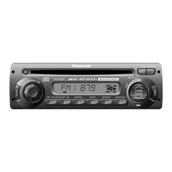
AUTOMOTIVE AFTERMARKET
CQ-5302U
Heavy Duty MP3 CD Player / Weather
Band Receiver with CD changer Control
/ Satellite Radio Ready
Weather Band Radio
Frequency Range
Usable Sensitivity
Signal to Noise Ratio (40 dB/µV)
CD Player
Sampling Frequency
DA Converter
Error Correction System
Pick-Up Type
Light Source
Wavelength
Frequency Response
Signal to Noise Ratio
Wow and Flutter
Channel Separation
Dimensions** (W×H×D)
Weight**
* Specifications and the design are subject to possible modification
without notice due to improvements.
** Dimensions and Weight shown are approximate.
© 2006 Matsushita Electric Industrial Co., Ltd. All
rights
reserved.
distribution is a violation of law.
Order No. ACED060432C1
162.40 - 162.55MHz
3dB/µV (S/N 20dB)
50dB
8 times oversampling
MASH 1 bit/4 DAC System
Spot size detection method
3-beam
Semiconductor Laser
790nm
20Hz to 20,000Hz (±1dB)
85dB
Below measurable limits
75 dB
7"×1-15/16×6-1/8"
(178×50×155mm)
3 lbs.12oz (1.7kg)
Unauthorized
copying
and
C4
Advertisement
Table of Contents

Related Manuals for Panasonic CQ-5302U


Summary of Contents for Panasonic CQ-5302U
- Page 1 Order No. ACED060432C1 AUTOMOTIVE AFTERMARKET CQ-5302U Heavy Duty MP3 CD Player / Weather Band Receiver with CD changer Control / Satellite Radio Ready Specification* General Power Supply DC 12V (11V - 16V), Weather Band Radio Test Voltage 14.4V Frequency Range 162.40 - 162.55MHz...
-
Page 2: Table Of Contents
CQ-5302U CONTENTS Page Page 1 ABOUT LEAD FREE SOLDER (PbF) 11 PACKAGE AND IC BLOCK DIAGRAM 2 LASER PRODUCTS 12 REPLACEMENT PARTS LIST 3 FEATUERS 13 EXPLODED VIEW (Unit) 4 REPLACEING THE FUSE 14 CD PLAYER MECHANICAL PARTS LIST 5 MAINTENANCE... -
Page 3: About Lead Free Solder (Pbf)
CQ-5302U 1 ABOUT LEAD FREE 3 FEATUERS • • • • 24-Stations Preset ( 6-FM1, 6-FM2 , 6-W/B , 6-AM ). SOLDER (PbF) • • • • Rotary VOL. Distinction of PbF PCB: • • • • Weather Band . -
Page 4: Wiring Connection
CQ-5302U 8 WIRING CONNECTION... -
Page 5: Block Diagram
CQ-5302U 9 BLOCK DIAGRAM... -
Page 6: Terminals Description
CQ-5302U 10 TERMINALS DESCRIPTION 10.1. Main Block IC601 : C2BBYY000199 Ref. Part Part Name & I/O(V Description Ref. Part Part Name & I/O(V PLL_COM Radio Description Communication clock CH_STB Changer Comunication Strobe PLL_CE Radio ROTARY2 Rotary encoder Communication Signal Input2(VOL... - Page 7 CQ-5302U Ref. Part Part Name & I/O(V Description CH-DATA CD Changer Comunication Data CH-CLK Changer Comunication Clock...
-
Page 8: Package And Ic Block Diagram
CQ-5302U 11 PACKAGE AND IC BLOCK DIAGRAM 11.1. Main Block IC401:C1BB00001037 IC201 : C1BB00000543... - Page 9 CQ-5302U IC251:C1EA00000042 IC701 : AN8065S-E1V IC501: C0CBCBG00012...
-
Page 10: Replacement Parts List
CQ-5302U 12 REPLACEMENT PARTS LIST Ref. Part No. Part Name & Description Remarks D651 B0BC5R600010 Zener Diode D652 B0BC5R600010 Zener Diode D653 B0BC5R600010 Zener Diode D654 B0BC5R600010 Zener Diode D661 B0JCCE000003 Diode D662 B0BC5R600010 Zener Diode D663 B0BC5R600010 Zener Diode... - Page 11 CQ-5302U Ref. Part No. Part Name & Description Remarks Ref. Part No. Part Name & Description Remarks C257 F1J1C105A173 Ceramic 1MFD 16WV C781 ECA1CM102L Electrolytic 1000PF 16WV C261 ECA1CDT472L Ceramic 4700PF 16WV C301 F1J1C105A173 Ceramic 1MFD 16WV DISPLAY BLOCK [E-4C299]...
- Page 12 CQ-5302U Ref. Part No. Part Name & Description Remarks Ref. Part No. Part Name & Description Remarks R282 D0GD123JA017 Chip 12k ohms 1/10W R654 D0GD102JA017 Chip 1k ohms 1/10W R301 D0GD102JA017 Chip 1k ohms 1/10W R655 D0GD102JA017 Chip 1k ohms 1/10W...
- Page 13 CQ-5302U Ref. Part No. Part Name & Description Remarks Ref. Part No. Part Name & Description Remarks FX0214C209YA Fix Plate 6. Electric Parts YFS014C030ZA Dust Sheet YFX014C090CA Back Light Assy YFV024C108CA Sheet SWITCHES YFS014C110CA Rubber Gum SW901 K0H1BA000445 Tack Swich...
-
Page 14: Exploded View (Unit)
CQ-5302U 13 EXPLODED VIEW (Unit) -
Page 15: Cd Player Mechanical Parts List
CQ-5302U 14 CD PLAYER MECHANICAL PARTS LIST Ref. Part No. Part Name & Description Remarks N(E-1) 3032 10 05 MODE SW WIRE N(A-1); N(E-1) 3032 10 09 SL WIRE N(C-1) N(E-1) 3033 10 11 WIRE HOLDER N(C-1) 1950 14 03 WIRE CLAMPER N(E-2);... -
Page 16: Exploded View (Cd Deck)
CQ-5302U 15 EXPLODED VIEW (CD Deck) -
Page 17: Packing Parts List
CQ-5302U 16 PACKING PARTS LIST .Item numbers listed below should not order reguler spare parts. (not available) Item No. Part No. Part Name & Description Q’ty Remarks Inner Carton Not available Packing Pad Front Not available Packing Pad Rear Not available... -
Page 18: Wiring Diagram
CQ-5302U 17 WIRING DIAGRAM 17.1. Main Block-1 [E-4C298][TOP VIEW] CQ-5302U Main PCB... - Page 19 CQ-5302U 17.2. Main Block-2 [E-4C298][BOTTOM VIEW] CQ-5302U Main PCB...
- Page 20 CQ-5302U 17.3. Display Block [E-4C299][TOP VIEW] [E-4C299][BOTTOM VIEW] CQ-5302U DISPLAY PCB...
-
Page 21: Schematic Diagram-1
4.56 2.97 5.17 4.96 4.56 9.16 4.56 5.07 13.5 4.56 5.08 8.17 4.56 9.15 8.16 4.57 4.56 5.08 5.14 4.56 5.12 0.81 12.9 8.14 0.14 0.14 0.01 1.19 5.04 5.22 2.51 2.46 1V/DIV.0.1uS/DIV 2V/DIV.0.1uS/DIV 5.24 4.83 2V/DIV.5mS/DIV CQ-5302U MAIN BLOCK... - Page 22 THIS PAGE IS JUST FOR THE PAGE LAYOUT USE ONLY.
-
Page 23: Schematic Diagram-2
CQ-5302U 19 SCHEMATIC DIAGRAM-2 19.1. Display Block... -
Page 24: Schematic Diagram For Printing With Letter Size
CQ-5302U 20 SCHEMATIC DIAGRAM for Printing with Letter Size 20.1. Main Block (Left Side) E-4C298 5.05 8.17 8.17 5.05 8.83 3.37 3.27 9.14 0.15 7.93 8.02 7.94 0.15 3.44 3.45 0.01 3.91 5.02 5.08 2.97 8.17 8.16 8.14 0.14 0.14 0.01... - Page 25 1.74 5.83 13.12 4.56 5.26 4.56 4.56 4.56 4.56 5.17 4.96 4.56 9.16 4.56 5.07 4.56 13.5 5.08 4.56 9.15 4.56 4.57 5.08 5.14 4.56 5.12 0.81 12.9 1V/DIV.0.1uS/DIV 2V/DIV.0.1uS/DIV 5.24 4.83 2V/DIV.5mS/DIV CQ-5302U MAIN BLOCK Printed in Taiwan 2006.04...