
Related Manuals for Quectel RM505Q-AE


Summary of Contents for Quectel RM505Q-AE
- Page 1 RM505Q-AE Hardware Design 5G Module Series Version: 1.0.0 Date: 2020-12-14 Status: Preliminary www.quectel.com...
- Page 2 To the maximum extent permitted by law, Quectel excludes all liability for any loss or damage suffered in connection with the use of the functions and features under development, regardless of whether such loss or damage may have been foreseeable.
- Page 3 RM505Q-AE Hardware Design Copyright The information contained here is proprietary technical information of Quectel. Transmitting, reproducing, disseminating and editing this document as well as using the content without permission are forbidden. Offenders will be held liable for payment of damages. All rights are reserved in the event of a patent grant or registration of a utility model or design.
-
Page 4: About The Document
5G Module Series RM505Q-AE Hardware Design About the Document Revision History Version Date Author Description Jared WANG 2020-10-20 Creation of the document Hank LIU Jared WANG/ 1.0.0 2020-12-14 Simon WANG/ Preliminary Hank LIU RM505Q-AE_Hardware_Design 3 / 79... -
Page 5: Table Of Contents
5G Module Series RM505Q-AE Hardware Design Contents About the Document ........................... 3 Contents ............................... 4 Table Index ..............................6 Figure Index ..............................7 Introduction ............................9 1.1. Safety Information ........................10 Product Concept ..........................11 2.1. General Description ........................11 2.2. - Page 6 5G Module Series RM505Q-AE Hardware Design GNSS Receiver ........................... 48 4.1. General Description ........................48 4.2. GNSS Performance ........................48 Antenna Interfaces ..........................50 5.1. Antenna Connectors ......................... 50 5.2. Cellular Antenna Port Mapping ....................51 5.3. Cellular Frequency ........................52 5.4.
- Page 7 5G Module Series RM505Q-AE Hardware Design Table Index Table 1: Frequency Bands and GNSS Systems of RM505Q-AE Module ..........11 Table 2: Key Features of RM505Q-AE ...................... 12 Table 3: Definition of I/O Parameters ......................18 Table 4: Pin Description ..........................18 Table 5: Overview of Operating Modes .....................
- Page 8 Figure 33: Coplanar Waveguide Design on a 4-layer PCB (Layer 4 as Reference Ground) ....57 Figure 34: RM505Q-AE RF Connector Dimensions (Unit: mm) ..............58 Figure 35: Specifications of Mating Plugs Using Ø 0.81 mm Coaxial Cables ........... 59 Figure 36: Connection between RF Connector and Mating Plug Using Ø...
- Page 9 5G Module Series RM505Q-AE Hardware Design Figure 42: Tray Packaging Procedure ....................... 76 RM505Q-AE_Hardware_Design 8 / 79...
-
Page 10: Introduction
5G Module Series RM505Q-AE Hardware Design Introduction This document introduces RM505Q-AE module and describes its air interface and hardware interfaces which are connected with customers’ applications. This document helps you quickly understand the interface specifications, electrical and mechanical details, as well as other related information of the module. To facilitate its application in different fields, reference design is also provided for reference. -
Page 11: Safety Information
Manufacturers of the cellular terminal should notify users and operating personnel of the following safety information by incorporating these guidelines into all manuals of the product. Otherwise, Quectel assumes no liability for customers’ failure to comply with these precautions. -
Page 12: Product Concept
It supports embedded operating systems such as Windows, Linux and Android, and also provides GNSS and voice functionality to meet specific application demands. The following table shows the frequency bands and GNSS systems of RM505Q-AE module. Table 1: Frequency Bands and GNSS Systems of RM505Q-AE Module... -
Page 13: Key Features
⚫ Smart metering system ⚫ Wireless router and switch ⚫ Other wireless terminal devices 2.2. Key Features The following table describes key features of RM505Q-AE. Table 2: Key Features of RM505Q-AE Feature Details ⚫ Function Interface PCI Express M.2 Interface ⚫... - Page 14 5G Module Series RM505Q-AE Hardware Design ⚫ Support QPSK, 16QAM and 64QAM modulation ⚫ DC-HSDPA: Max 42 Mbps (DL) ⚫ HSUPA: Max 5.76 Mbps (UL) ⚫ WCDMA: Max 384 kbps (DL)/384 kbps (UL) ⚫ Internet Protocol QMI/NTP* protocols ⚫ Features The protocols PAP and EIRP usually used for PPP connections ⚫...
- Page 15 5G Module Series RM505Q-AE Hardware Design NOTES HPUE is only for single carrier. To meet this operating temperature range, you need to ensure effective thermal dissipation, for example, by adding passive or active heatsinks, heat pipes, vapor chambers, etc. Within this range, the module can meet 3GPP specifications.
-
Page 16: Functional Diagram
Figure 1: Functional Block Diagram 2.4. Evaluation Board To help you develop applications conveniently with RM505Q-AE, Quectel supplies an evaluation board (PCIe Card EVB), a USB to RS-232 converter cable, a USB type-C cable, antennas and other peripherals to control or test the module. For more details, see document [1]. -
Page 17: Application Interfaces
5G Module Series RM505Q-AE Hardware Design Application Interfaces The physical connections and signal levels of RM505Q-AE comply with PCI Express M.2 specification. This chapter mainly describes the definition and application of the following interfaces/pins of RM505Q-AE: ⚫ Power supply ⚫... -
Page 18: Pin Assignment
5G Module Series RM505Q-AE Hardware Design 3.1. Pin Assignment The following figure shows the pin assignment of RM505Q-AE. The top side contains RM505Q-AE module and antenna connectors. Pin Name Pin Name CONFIG_2 CONFIG_1 AP2SDX_STATUS RESET_N USIM1_DET RFFE_VIO_1V8 COEX_TXD ANTCTL2 COEX_RXD... -
Page 19: Pin Description
Analog Input Analog Output Digital Input Digital Output Bidirectional Open Drain Power Input Power Output The following table shows the pin definition and description of RM505Q-AE. Table 4: Pin Description Pin No. Pin Name Description Comment CONFIG_3 Not connected internally = 3.135 V... - Page 20 5G Module Series RM505Q-AE Hardware Design turned off. When it is at high voltage level, the module is turned on. Requires differential USB_DP USB differential data (+) impedance of 90 Ω 1.8/3.3 V power domain. W_DISABLE1# Airplane mode control. Active LOW.
- Page 21 5G Module Series RM505Q-AE Hardware Design PCM_SYNC* PCM data frame sync 1.8 V power domain USB 3.1 super-speed Requires differential USB_SS_TX_M impedance of 90 Ω transmit (-) USIM1_RST (U)SIM1 card reset 1.8/3.0 V power domain USB 3.1 super-speed Requires differential USB_SS_TX_P impedance of 90 Ω...
- Page 22 5G Module Series RM505Q-AE Hardware Design Ground Open drain PCIE_CLKREQ_N PCIe clock request. Active LOW. 100 MHz. PCIE_REFCLK_M PCIe reference clock (-) Requires differential impedance of 85 Ω Open drain PCIE_WAKE_N PCIe wake up. Active LOW. 100 MHz. PCIE_REFCLK_P PCIe reference clock (+) Requires differential impedance of 85 Ω...
-
Page 23: Operating Modes
5G Module Series RM505Q-AE Hardware Design = 3.7 V norm = 4.4 V Ground Vmin = 3.135 V Power supply Vnorm = 3.7 V Vmax = 4.4 V Ground Vmin = 3.135 V Power supply Vnorm = 3.7 V Vmax = 4.4 V... -
Page 24: Power Supply
5G Module Series RM505Q-AE Hardware Design In this mode, the power management unit shuts down the power supply. Software is Power Down inactive, the serial interfaces are inaccessible, and the operating voltage (connected to Mode VCC) remains applied. 3.4. Power Supply The following table shows pin definition of VCC pins and ground pins. -
Page 25: Reference Design For Power Supply
5G Module Series RM505Q-AE Hardware Design circuit for the VCC. Figure 4: Reference Circuit for VCC Pins 3.4.2. Reference Design for Power Supply Power design is critical as the module’s performance largely depends on its power source. The power supply of the module should be able to provide a sufficient current of 3.0 A at least. If the voltage difference between input and output is not too big, use an LDO when supplying power to the module. -
Page 26: Turn On And Off Scenarios
5G Module Series RM505Q-AE Hardware Design 3.5. Turn on and off Scenarios 3.5.1. Turn on the Module FULL_CARD_POWER_OFF# asynchronous signal is an active low input that is used to turn on/off the entire module. When the input signal is asserted high (≥ 1.19 V) the module will be turned on. When the input signal is driven low (≤... -
Page 27: Turn Off The Module
5G Module Series RM505Q-AE Hardware Design It is recommended to use a host GPIO to control FULL_CARD_POWER_OFF# to turn on the module. A simple reference circuit is illustrated as the following figure. Host Module 1.8 V or 3.3 V FULL_CARD_POWER_OFF#... -
Page 28: Turn Off The Module Through At Command
5G Module Series RM505Q-AE Hardware Design RESET_N(H) FULL_CARD_POWER_OFF# ≥10 s Module Status RUNNING Power-off procedure Figure 8: Turn-off Timing through FULL_CARD_POWER_OFF# 3.5.2.2. Turn off the Module through AT Command It is also a safe way to use AT+QPOWD command to turn off the module. For more details about the command, see document [2]. - Page 29 5G Module Series RM505Q-AE Hardware Design the module will be immediately placed in a Power On Reset (POR) condition. CAUTION: Triggering the RESET# signal will lead to the loss of all data in the modem and the removal of system drivers. It will also disconnect the modem from the network.
- Page 30 5G Module Series RM505Q-AE Hardware Design Host Module VDD 1.5 V 100K RESET_N Reset pulse Reset Logic GPIO NMOS 200-700 ms 100K Figure 11: Reference Circuit for RESET_N with NMOS Driving Circuit Module VDD 1.5 V 100K RESET_N Reset Logic...
-
Page 31: U)Sim Interfaces
5G Module Series RM505Q-AE Hardware Design Figure 13: Resetting Timing of the Module 3.7. (U)SIM Interfaces The (U)SIM interfaces circuitry meets ETSI and IMT-2000 requirements. Both Class B (3.0 V) and Class C (1.8 V) (U)SIM cards are supported, and Dual SIM Single Standby* function is supported. - Page 32 NOTE “*” means under development. RM505Q-AE supports (U)SIM card hot-plug via the USIM_DET pin. With a normally closed (U)SIM card connector, the USIM_DET is normally short-circuited to ground when a (U)SIM card is not inserted, and the USIM_DET will change from low to high voltage level when a (U)SIM card is inserted. The rising edge indicates an insertion of the (U)SIM card.
- Page 33 5G Module Series RM505Q-AE Hardware Design USIM_VDD Module (U)SIM Card Connector 100 nF 10-20k USIM_VDD 1.8 V USIM_RST USIM_CLK 4.7k USIM_DET USIM_DATA Note: All these resistors, capacitors and TVS should be close to (U)SIM card connector in PCB layout. Figure 15: Reference Circuit for Normally Open (U)SIM Card Connector If (U)SIM card detection function is not needed, please keep USIM_DET disconnected.
-
Page 34: Usb Interface
5G Module Series RM505Q-AE Hardware Design potential. ⚫ To avoid cross-talk between USIM_DATA and USIM_CLK, keep them away from each other and shield them with surrounded ground. ⚫ To offer better ESD protection, add a TVS diode array of which the parasitic capacitance should be not higher than 10 pF. - Page 35 5G Module Series RM505Q-AE Hardware Design For more details about the USB 3.1 & 2.0 specifications, please visit http://www.usb.org/home. The USB 2.0 interface is recommended to be reserved for firmware upgrade in designs. The following figure shows a reference circuit for USB 3.1/2.0 interface.
-
Page 36: Pcie Interface
5G Module Series RM505Q-AE Hardware Design 3.9. PCIe Interface RM505Q-AE provides one integrated PCIe (Peripheral Component Interconnect Express) interface which complies with the PCI Express Base Specification, Revision 3.0 and supports up to 8 Gbps per lane. ⚫ PCI Express Base Specification, Revision 3.0 compliant ⚫... - Page 37 5G Module Series RM505Q-AE Hardware Design Host Module PCIE_REFCLK_P PCIE_REFCLK_P PCIE_REFCLK_M PCIE_REFCLK_M PCIE_RX_P C5 220 nF PCIE_TX_P PCIE_RX_M C6 220 nF PCIE_TX_M PCIE_TX_P C1 220 nF PCIE_RX_P PCIE_TX_M C2 220 nF PCIE_RX_M VCC_IO_HOST 100k 100k 100k PCIE_WAKE_N PCIE_WAKE_N PCIE_CLKREQ_N PCIE_CLKREQ_N...
- Page 38 5G Module Series RM505Q-AE Hardware Design Figure 19: PCIe Power-on Timing Requirements of M.2 Specification Module power-on or insertion detection power -on FUL L_CARD_ POWER_OFF System turn-on and booting 1.19 V 68 ms RESET_N turn-on RFFE_ VIO _1V8 23 ms...
-
Page 39: Usb And Pcie Modes
Supports Non-X86 systems and X86 system (supports BIOS PCIe early initial) RM505Q-AE can also be reprogrammed to PCIe mode based on eFuse. If the communication is switched to PCIe mode by burnt eFuse, the communication cannot be switched back to USB mode. -
Page 40: Pcm Interface
256 kHz PCM_CLK and an 8 kHz PCM_SYNC of 50 % duty cycle only. RM505Q-AE supports 16-bit linear data format. The following figures show the primary mode’s timing relationship with 8 kHz PCM_SYNC and 2048 kHz PCM_CLK, as well as the auxiliary mode’s timing relationship with 8 kHz PCM_SYNC and 256 kHz PCM_CLK. - Page 41 5G Module Series RM505Q-AE Hardware Design 125 μs PCM_CLK PCM_SYNC PCM_DOUT PCM_DIN Figure 22: Auxiliary Mode Timing The following table shows the pin definition of PCM interface which can be applied to audio codec design. Table 12: Pin Definition of PCM Interface Pin No.
-
Page 42: Control And Indication Interfaces
“*” means under development. 3.11.1. W_DISABLE1# RM505Q-AE provides a W_DISABLE1# pin to disable or enable airplane mode through hardware method. The W_DISABLE1# pin is pulled up by default. Driving it low will set the module to airplane mode. In airplane mode, the RF function will be disabled. -
Page 43: W_Disable2
AT+CFUN=4 3.11.2. W_DISABLE2# RM505Q-AE provides a W_DISABLE2# pin to disable or enable the GNSS function. The W_DISABLE2# pin is pulled up by default. Driving it low will disable the GNSS function. The combination of W_DISABLE2# pin and AT commands controls the GNSS function. -
Page 44: Wwan_Led
5G Module Series RM505Q-AE Hardware Design Host Module VCC_IO_HOST VDD 1.8 V 100k 100k W_DISABLE2# GPIO W_DISABLE1# GPIO Note: The voltage level of VCC_IO_HOST could be 1.8 V or 3.3 V typically. Figure 23: W_DISABLE1# and W_DISABLE2# Reference Circuit 3.11.3. WWAN_LED#* The WWAN_LED# signal is used to indicate the RF status of the module, and its sink current is up to 10 mA. -
Page 45: Wake_On_Wan
5G Module Series RM505Q-AE Hardware Design Table 16: Network Status Indications of WWAN_LED# Signal WWAN_LED# Logic Level Description Low (LED on) RF function is turned on RF function is turned off if any of the following occurs: ⚫ The (U)SIM card is not powered. -
Page 46: Dpr
RM505Q-AE provides a DPR (Dynamic Power Reduction) pin for body SAR (Specific Absorption Rate) detection. The signal is sent from the proximity sensor of a host system to RM505Q-AE module to provide an input trigger, which will reduce the output power in radio transmission. -
Page 47: Antenna Tuner Control Interface
5G Module Series RM505Q-AE Hardware Design Notification from WLAN to SDR while WLAN_TX_EN 1.8 V power domain transmitting NOTE “*” means under development. 3.13. Antenna Tuner Control Interface* ANTCTL[1:2] and RFFE signals are used for antenna tuner control and should be routed to an appropriate antenna control circuit. -
Page 48: Configuration Pins
5G Module Series RM505Q-AE Hardware Design 3.14. Configuration Pins RM505Q-AE provides four configuration pins, which are defined as below. Table 21: Definition of Configuration Pins Pin No. Pin Name Power Domain Description CONFIG_0 Not connected internally CONFIG_1 Connected to GND internally... -
Page 49: Gnss Receiver
GNSS Receiver 4.1. General Description RM505Q-AE includes a fully integrated global navigation satellite system solution that supports Gen9-Lite of Qualcomm (GPS, GLONASS, BeiDou/Compass, and Galileo). The module supports standard NMEA-0183 protocol, and outputs NMEA sentences at 1 Hz data update rate via USB interface by default. - Page 50 5G Module Series RM505Q-AE Hardware Design Autonomous Hot start @ open sky XTRA enabled Accuracy Autonomous CEP-50 (GNSS) @ open sky NOTES Tracking sensitivity: the minimum GNSS signal power at which the module can maintain locked (keep positioning for at least 3 minutes continuously).
-
Page 51: Antenna Interfaces
5G Module Series RM505Q-AE Hardware Design Antenna Interfaces RM505Q-AE provides five antenna interfaces, the impedance of each antenna port is 50 Ω. 5.1. Antenna Connectors The ANT0, ANT1, ANT2,ANT3 and ANT4_GNSS antenna connectors are shown by the following figure. ANT0 ANT1... -
Page 52: Cellular Antenna Port Mapping
5G Module Series RM505Q-AE Hardware Design Table 24: RF Bands Supported by RM505Q-AE Antenna Connectors Pin Name I/O Description Comment LTE MHB TRx0; LTE UHB PRx MIMO 50 Ω impedance ANT0 AI/AO 5G FDD/TDD MHB TRx0; 5G NR n77/n78/n79 PRx MIMO;... -
Page 53: Cellular Frequency
AI/AO 5G FDD/TDD MHB DRx; 5G NR n77/n78/n79 DRx; ANT4_ 50 Ω impedance GNSS L1 & L5 Rx GNSS 5.3. Cellular Frequency Table 26: RM505Q-AE Module Operating Frequencies Band Name Transmit (MHz) Receive (MHz) LTE-FDD LTE-TDD UMTS 5G NR –... -
Page 54: Gnss Frequency
5G Module Series RM505Q-AE Hardware Design – – – 704–716 734–746 – – – 815–830 860–875 – – 830–845 875–890 – – EU800 832–862 791–821 – – PCS + G 1850–1915 1930–1995 – – – 814–849 859–894 – – 700 APAC 703–748... - Page 55 5G Module Series RM505Q-AE Hardware Design Table 27: GNSS Frequency Type Frequency Unit 1575.42± 1.023 (GPS L1) GPS/Galileo/QZSS 1176.45± 10.23 (GPS L5) Galileo 1575.42 ± 2.046 (E1) QZSS 1575.42 (L1) GLONASS 1597.5–1605.8 BeiDou 1561.098 ± 2.046 VDD 1.7 V GNSS Antenna...
-
Page 56: Reference Design For Cellular Antenna Interfaces
5G Module Series RM505Q-AE Hardware Design 5.5. Reference Design for Cellular Antenna Interfaces A reference design for cellular antenna interface is shown as below. A π-type matching circuit should be reserved for better cellular RF performance. The capacitors are not mounted by default. -
Page 57: Reference Design Of Rf Layout
5G Module Series RM505Q-AE Hardware Design 5.6. Reference Design of RF Layout For user’s PCB, the characteristic impedance of all RF traces should be controlled to 50 Ω. The impedance of the RF traces is usually determined by the trace width (W), the materials’ dielectric constant, the height from the reference ground to the signal layer (H), and the spacing between RF traces and grounds (S). - Page 58 5G Module Series RM505Q-AE Hardware Design Figure 33: Coplanar Waveguide Design on a 4-layer PCB (Layer 4 as Reference Ground) In order to ensure RF performance and reliability, the following principles should be complied with in RF layout design: ⚫...
-
Page 59: Antenna Installation
LTE HB, 5G NR TDD MHB: Cable insertion loss < 2 dB 5.7.2. Recommended RF Connector for Antenna Installation RM505Q-AE is mounted with standard 2.0 mm × 2.0 mm receptacle RF connectors for convenient antenna connection. The connector dimensions are illustrated as below:... - Page 60 Max 1.45 (3–6 GHz) The receptacle RF connector used in conjunction with RM505Q-AE will accept two types of mating plugs that will meet a maximum height of 1.2 mm using a Ø 0.81 mm coaxial cable or a maximum height of 1.45 mm utilizing a Ø...
- Page 61 5G Module Series RM505Q-AE Hardware Design The following figure illustrates the connection between the receptacle RF connector on RM505Q-AE and the mating plug using a Ø 0.81 mm coaxial cable. Figure 36: Connection between RF Connector and Mating Plug Using Ø 0.81 mm Coaxial Cable The following figure illustrates the connection between the receptacle RF connector on RM505Q-AE and the mating plug using a Ø...
-
Page 62: Reliability, Radio And Electrical Characteristics
Voltage at Digital Pins -0.3 6.2. Power Supply Requirements The typical input voltage of RM505Q-AE is 3.7 V, as specified by PCIe M.2 Electromechanical Specification Rev 1.0. The following table shows the power supply requirements of RM505Q-AE. Table 31: Power Supply Requirements... -
Page 63: I/O Requirements
5G Module Series RM505Q-AE Hardware Design 6.3. I/O Requirements Table 32: I/O Requirements Parameter Description Min. Max. Unit Input high voltage 0.7 × V +0.3 DD18 DD18 Input low voltage -0.3 0.3 × V DD18 Output high voltage -0.5 DD18... -
Page 64: Current Consumption
, may undergo a reduction in value, exceeding the specified tolerances of 3GPP. When the temperature returns to the normal operating temperature level, the module will meet 3GPP specifications again. 6.5. Current Consumption Table 34: RM505Q-AE Current Consumption Description Conditions Typ. - Page 65 5G Module Series RM505Q-AE Hardware Design transfer (GNSS WCDMA B1 HSUPA CH10700 @ 23 dBm OFF) WCDMA B2 HSDPA CH9800 @ 23 dBm WCDMA B2 HSUPA CH9800 @ 23 dBm WCDMA B3 HSDPA CH1338 @ 23 dBm WCDMA B3 HSUPA CH1338 @ 23 dBm...
- Page 66 5G Module Series RM505Q-AE Hardware Design LTE-FDD B17 CH5790 @ 23 dBm LTE-FDD B18 CH5925 @ 23 dBm LTE-FDD B19 CH6075 @ 23 dBm LTE-FDD B20 CH6300 @ 23 dBm LTE-FDD B25 CH8365 @ 23 dBm LTE-FDD B26 CH8865 @ 23 dBm...
- Page 67 5G Module Series RM505Q-AE Hardware Design 5G NR-TDD n78 CH652666 @ 23 dBm 5G NR-TDD n79 CH695090 @ 23 dBm 5G NR-TDD n79 CH713522 @ 23 dBm 5G NR-TDD n79 CH731976 @ 23 dBm 5G NR-FDD n1 CH423000 @ 23 dBm...
- Page 68 5G Module Series RM505Q-AE Hardware Design 5G NR-FDD n20 CH161200 @ 23 dBm 5G NR-FDD n20 CH163200 @ 23 dBm 5G NR-FDD n25 CH387000 @ 23 dBm 5G NR-FDD n25 CH392500 @ 23 dBm 5G NR-FDD n25 CH398000 @ 23 dBm...
-
Page 69: Rf Output Power
5G Module Series RM505Q-AE Hardware Design WCDMA B8 CH3012 @ 23 dBm WCDMA B19 CH338 @ 23 dBm 6.6. RF Output Power The following table shows the RF output power of RM505Q-AE module. Table 35: RF Output Power Mode Frequency Max. - Page 70 5G Module Series RM505Q-AE Hardware Design WCDMA B2 -104.7 dBm WCDMA B3 -103.7 dBm WCDMA B4 -106.7 dBm WCDMA B5 -104.7 dBm WCDMA B8 -103.7 dBm WCDMA B19 -104.7 dBm LTE-FDD B1 (10 MHz) -96.3 dBm LTE-FDD B2 (10 MHz) -94.3 dBm...
- Page 71 5G Module Series RM505Q-AE Hardware Design LTE-FDD B32 (10 MHz) -95.3 dBm LTE-TDD B34 (10 MHz) -96.3 dBm LTE-TDD B38 (10 MHz) -96.3 dBm LTE-TDD B39 (10 MHz) -96.3 dBm LTE-TDD B40 (10 MHz) -96.3 dBm LTE-TDD B41 (10 MHz) -94.3 dBm...
-
Page 72: Esd Characteristics
5G Module Series RM505Q-AE Hardware Design 5G NR-TDD n41 (20 MHz) -92.0 dBm (SCS: 30 kHz) 5G NR-FDD n66 (20 MHz) -93.5 dBm (SCS: 15 kHz) 5G NR-FDD n71 (10 MHz) -94.0 dBm (SCS: 15 kHz) 5G NR-TDD n77 (20 MHz) -92.9 dBm... -
Page 73: Thermal Dissipation
RM505Q-AE Hardware Design 6.9. Thermal Dissipation RM505Q-AE is designed to work over an extended temperature range. To achieve a maximum performance while working under extended temperatures or extreme conditions (such as with maximum power or data rate) for a long time, it is strongly recommended to add a thermal pad or other thermally conductive compounds between the module and the main PCB for thermal dissipation. - Page 74 5G Module Series RM505Q-AE Hardware Design between the heatsink and the module, and the heatsink should be designed with as many fins as possible to increase the heat dissipation area. NOTE If a conformal coating is necessary for the module, do NOT use any coating material that may chemically react with the PCB or shielding cover, and prevent the coating material from flowing into the module.
-
Page 75: Mechanical Dimensions And Packaging
RM505Q-AE Hardware Design Mechanical Dimensions and Packaging This chapter mainly describes mechanical dimensions and packaging specifications of RM505Q-AE module. All dimensions are measured in mm, and the tolerances are ± 0.05 mm unless otherwise specified. 7.1. Mechanical Dimensions of the Module... -
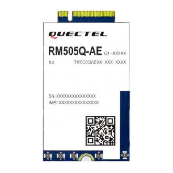
Page 76: Top And Bottom Views Of The Module
Images above are for illustration purpose only and may differ from the actual module. For authentic appearance and label, please refer to the module received from Quectel. 7.3. M.2 Connector RM505Q-AE adopts a standard PCI Express M.2 connector which compiles with the directives and standards listed in document [5]. 7.4. Packaging RM505Q-AE modules are packaged in trays. - Page 77 5G Module Series RM505Q-AE Hardware Design Figure 41: Tray Size (Unit: mm) Each tray contains 10 modules. The smallest package contains 100 modules. Tray packaging procedures are as below. 1. Use 10 trays to package 100 modules at a time (tray size: 247 mm × 172 mm).
-
Page 78: Appendix References
5G Module Series RM505Q-AE Hardware Design Appendix References Table 38: Related Documents Document Name Description Quectel_PCIe_Card_EVB_User_Guide PCIe card EVB user guide Quectel_RG50xQ&RM5xxQ_Series_AT_Commands_ AT commands manual for Manual RG50xQ and RM5xxQ Quectel_RG50xQ&RM5xxQ_Series_GNSS_Application_ The GNSS application note for Note RG50xQ and RM5xxQ series... - Page 79 5G Module Series RM505Q-AE Hardware Design GNSS Global Navigation Satellite System Global Positioning System GRFC Generic RF Control Global System for Mobile Communications HPUE High Power User Equipment HSPA High Speed Packet Access HSUPA High Speed Uplink Packet Access kbps...
- Page 80 5G Module Series RM505Q-AE Hardware Design Point-to-Point Protocol Qualcomm MSM (Mobile Station Modems) Interface Root Complex Radio Frequency RFFE RF Front-End R/LHCP Right/Left Hand Circular Polarization Receive Specific Absorption Rate Subcarrier Spacing Software-Defined Radio SIMO Single-Input Multiple-Output Short Message Service...
- Page 81 Quectel that they wish to change the antenna trace design. In this case, a Class II permissive change application is required to be filed by...
- Page 82 Antenna (1) The antenna must be installed such that 20 cm is maintained between the antenna and users, (2) The transmitter module may not be co-located with any other transmitter or antenna. In the event that these conditions cannot be met (for example certain laptop configurations or co-location with another transmitter), then the FCC/IC authorization is no longer considered valid and the FCC ID/IC ID cannot be used on the final product.
- Page 83 Federal Communication Commission Interference Statement This device complies with Part 15 of the FCC Rules. Operation is subject to the following two conditions: (1) This device may not cause harmful interference, and (2) this device must accept any interference received, including interference that may cause undesired operation. This equipment has been tested and found to comply with the limits for a Class B digital device, pursuant to Part 15 of the FCC Rules.
- Page 84 This device is intended only for OEM integrators under the following conditions: (For module device use) 1) The antenna must be installed such that 20 cm is maintained between the antenna and users, and 2) The transmitter module may not be co-located with any other transmitter or antenna. As long as 2 conditions above are met, further transmitter test will not be required.
- Page 85 Industry Canada Statement This device complies with Industry Canada’s licence-exempt RSSs. Operation is subject to the following two conditions: (1) This device may not cause interference; and (2) This device must accept any interference, including interference that may cause undesired operation of the device.
- Page 86 Cet appareil est conçu uniquement pour les intégrateurs OEM dans les conditions suivantes: (Pour utilisation de dispositif module) 1) L'antenne doit être installée de telle sorte qu'une distance de 20 cm est respectée entre l'antenne et les utilisateurs, et 2) Le module émetteur peut ne pas être coïmplanté avec un autre émetteur ou antenne. Tant que les 2 conditions ci-dessus sont remplies, des essais supplémentaires sur l'émetteur ne seront pas nécessaires.
- Page 87 Manual Information to the End User The OEM integrator has to be aware not to provide information to the end user regarding how to install or remove this RF module in the user’s manual of the end product which integrates this module. The end user manual shall include all required regulatory information/warning as show in this manual.
Need help?
Do you have a question about the RM505Q-AE and is the answer not in the manual?
Questions and answers