
Related Manuals for Quectel Smart Module Series


Summary of Contents for Quectel Smart Module Series
- Page 1 SA800U-WF Hardware Design Smart Module Series Version: 1.0 Date: 2021-01-13 Status: Released www.quectel.com...
- Page 2 To the maximum extent permitted by law, Quectel excludes all liability for any loss or damage suffered in connection with the use of the functions and features under development, regardless of whether such loss or damage may have been foreseeable.
- Page 3 SA800U-WF Hardware Design Copyright The information contained here is proprietary technical information of Quectel. Transmitting, reproducing, disseminating and editing this document as well as using the content without permission are forbidden. Offenders will be held liable for payment of damages. All rights are reserved in the event of a patent grant or registration of a utility model or design.
-
Page 4: Safety Information
Manufacturers of the cellular terminal should notify users and operating personnel of the following safety information by incorporating these guidelines into all manuals of the product. Otherwise, Quectel assumes no liability for customers’ failure to comply with these precautions. -
Page 5: About The Document
Smart Module Series SA800U-WF Hardware Design About the Document Revision History Version Date Author Description Light WANG/ 2020-07-31 Creation of the document Finley ZHANG Light WANG/ 2021-01-13 First official release Finley ZHANG SA800U-WF_Hardware_Design 4 / 106... -
Page 6: Table Of Contents
Smart Module Series SA800U-WF Hardware Design Contents Safety Information ............................3 About the Document ........................... 4 Contents ............................... 5 Table Index ..............................7 Figure Index ..............................9 Introduction ............................10 Product Concept ..........................11 2.1. General Description ........................11 2.2. - Page 7 Smart Module Series SA800U-WF Hardware Design 3.18. LCM Interfaces .......................... 63 3.19. Touch Panel Interface ....................... 67 3.20. Camera Interfaces........................68 3.20.1. Design Considerations ....................73 3.20.2. Flashlight Interfaces ....................... 77 3.21. Sensor Interfaces ........................78 3.22. Audio Interfaces ........................79 3.23.
- Page 8 Smart Module Series SA800U-WF Hardware Design Table Index Table 1: SA800U-WF Frequency Bands .....................11 Table 2: SA800U-WF Key Features ......................12 Table 3: I/O Parameters Definition ......................18 Table 4: Pin Description ..........................18 Table 5: Power Description ........................44 Table 6: Pin Definition of Charging Interface .....................
- Page 9 Smart Module Series SA800U-WF Hardware Design Table 42: Tray Package ..........................101 Table 43: Related Documents ........................102 Table 44: Terms and Abbreviations ......................102 SA800U-WF_Hardware_Design 8 / 106...
- Page 10 Smart Module Series SA800U-WF Hardware Design Figure Index Figure 1: Functional Diagram ........................15 Figure 2: Pin Assignment (Top View) ......................17 Figure 3: Voltage Drop Sample ........................38 Figure 4: Star Structure of Power Supply ....................39 Figure 5: Reference Circuit of Power Supply ..................... 39 Figure 6: Turn on the Module Using Driving Circuit ...................
-
Page 11: Introduction
Smart Module Series SA800U-WF Hardware Design Introduction This document defines the SA800U-WF module and describes its air interfaces and hardware interfaces. This document helps you quickly understand module interface specifications, electrical and mechanical details as well as other related information of the module. Associated with application notes and user guides, you can use the module to design and set up applications easily. -
Page 12: Product Concept
Smart Module Series SA800U-WF Hardware Design Product Concept 2.1. General Description SA800U-WF is a smart module based on Qualcomm platform and Android operating system, which provides industrial grade performance. Its general features are listed below: Support short-range wireless communication via Wi-Fi 802.11a/b/g/n/ac and BT 5.0 ... -
Page 13: Key Features
Smart Module Series SA800U-WF Hardware Design 2.2. Key Features The following table describes the detailed features of the module. Table 2: SA800U-WF Key Features Features Details 64-bit Kryo 385 applications processor Quad high-performance Kyro cores at 2.649 GHz with 256 KB L2 cache... - Page 14 Smart Module Series SA800U-WF Hardware Design 2 USB interfaces which comply with both USB 3.1 and USB 2.0 specifications Support up to 5 Gbps on USB 3.1 and 480 Mbps on USB 2.0 USB Interfaces USB1 supports USB OTG and DisplayPort, and can be used for AT...
-
Page 15: Functional Diagram
Smart Module Series SA800U-WF Hardware Design NOTES The 2-lane MIPI CSI can only get data of RAW format. It can be used for ToF/3D camera modules but cannot be used for display. Within the operating temperature range, the module is IEEE compliant. -
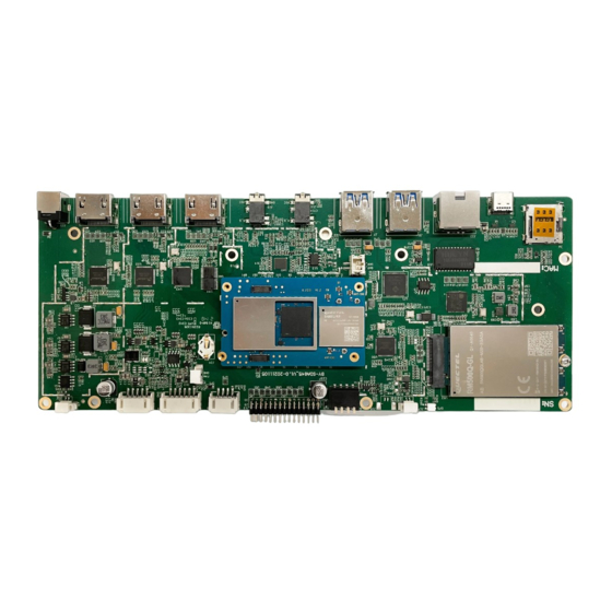
Page 16: Evaluation Board
Figure 1: Functional Diagram 2.4. Evaluation Board To help you develop applications with SA800U-WF conveniently, Quectel supplies the evaluation board, USB to RS-232 converter cable, USB Type-C data cable, power adapter, earphone, antenna and other peripherals to control or test the module. For more details, see document [1]. -
Page 17: Application Interfaces
Smart Module Series SA800U-WF Hardware Design Application Interfaces 3.1. General Description SA800U-WF is equipped with 396 pins that can be embedded into cellular application platform. The following chapters provide the detailed description of interfaces listed below. Power supply ... -
Page 18: Pin Assignment
Smart Module Series SA800U-WF Hardware Design 3.2. Pin Assignment The following figure shows the pin assignment of SA800U-WF module. J1-2 J1-1 J2-2 J2-1 J1-4 J1-3 J2-4 J2-3 J1-6 J1-5 J2-6 J2-5 J1-8 J2-8 J1-10 J2-10 J1-12 J2-12 J1-14 J2-14 J1-16... -
Page 19: Pin Description
Smart Module Series SA800U-WF Hardware Design 3.3. Pin Description Table 3: I/O Parameters Definition Type Description Analog Input Analog Output Analog Input/Output Digital Input Digital Output Digital Input/Output Open Drain Power Input Power Output The following tables show the SA800U-WF’s pin definitions and electrical characteristics. - Page 20 Smart Module Series SA800U-WF Hardware Design Power supply for J2-124, external GPIO’s Vnom = 1.8 V VREG_S4A_1V8 J2-126, 1.8 V output max = 2000 mA pull-up circuit and J2-128 level shift circuit. Power supply for IOVDD of cameras. Add a 1.0–4.7 μF Vnom = 1.8 V...
- Page 21 Smart Module Series SA800U-WF Hardware Design Power supply for DP’s pull-up circuits. Add a 1.0–4.7 μF Vnom = 3.075 V LDO24A_3V075 J4-8 3.075 V output max = 150 mA bypass capacitor if used. If unused, keep this pin open. Power supply for VDD of TP.
- Page 22 Smart Module Series SA800U-WF Hardware Design USB1 3.1 channel 1 USB1_SS1_TX_M J2-123 super-speed transmit (-) USB1 3.1 channel 1 USB1_SS1_TX_P J2-125 super-speed transmit (+) USB1 3.1 channel 1 USB1_SS1_RX_M J2-118 super-speed receive (-) USB1 3.1 channel 1 USB1_SS1_RX_P J2-120 90 Ω differential...
- Page 23 Smart Module Series SA800U-WF Hardware Design USB2 2.0 compliant. USB2_DM J2-107 differential data Only support host mode. USB2 3.1 channel 1 USB2_SS_TX_M J2-108 super-speed transmit (-) USB2 3.1 90 Ω differential channel 1 USB2_SS_TX_P J2-106 super-speed impedance. transmit (+) USB 3.1 standard compliant.
- Page 24 Smart Module Series SA800U-WF Hardware Design PCIe1 wake up max = 0.63 V PCIE1_WAKE_N J1-111 host min = 1.17 V PCIe1 clock max = 0.63 V PCIE1_CLKREQ_N J1-109 request min = 1.17 V PCIe1 reference PCIE1_REFCLK_P J1-121 clock (+) PCIe1 reference...
- Page 25 Smart Module Series SA800U-WF Hardware Design max = 0.58 V SD_DATA1 J1-53 SDIO data bit 1 min = 1.27 V max = 0.45 V SD_DATA2 J1-57 SDIO data bit 2 min = 1.4 V 2.95 V SD card: max = 0.73 V...
- Page 26 Smart Module Series SA800U-WF Hardware Design Display bias VDISP_P J4-29 output (+) Display bias VDISP_M J4-30 output (-) Active low. max = 0.45 V LCD_RST J2-62 LCD reset 1.8 V power min = 1.35 V domain. LCD tearing max = 0.63 V 1.8 V power...
- Page 27 Smart Module Series SA800U-WF Hardware Design LCD1 MIPI lane DSI1_LN2_N J2-27 2 data (-) LCD1 MIPI lane DSI1_LN2_P J2-25 2 data (+) LCD1 MIPI lane DSI1_LN3_N J2-31 3 data (-) LCD1 MIPI lane DSI1_LN3_P J2-33 3 data (+) Camera Interfaces Pin Name Pin No.
- Page 28 Smart Module Series SA800U-WF Hardware Design MIPI lane 1 data CSI1_LN1_P J1-48 of camera 1 (+) MIPI lane 2 data CSI1_LN2_N J1-42 of camera 1 (-) MIPI lane 2 data CSI1_LN2_P J1-40 of camera 1 (+) MIPI lane 3 data...
- Page 29 Smart Module Series SA800U-WF Hardware Design Master clock of CAM0_MCLK J1-91 camera 0 Master clock of CAM1_MCLK J1-95 camera 1 Master clock of CAM2_MCLK J1-99 camera 2 Master clock of CAM3_MCLK J1-103 camera 3 Strobe of CAM0_STROBE J1-122 camera 0...
- Page 30 Smart Module Series SA800U-WF Hardware Design DVDD enable of CAM2_DVDD_EN J1-110 camera 2 DVDD enable of CAM3_DVDD_EN J1-128 camera 3 CCI0_I2C_SCL J1-142 CCI0 I2C clock CCI0_I2C_SDA J1-144 CCI0 I2C data 1.8 V power domain. CCI1_I2C_SDA J1-146 CCI1 I2C data CCI1_I2C_SCL...
- Page 31 Smart Module Series SA800U-WF Hardware Design Sensor core SSC_SPI1_MOSI J1-152 SPI1 master-out slave-in Sensor core max = 0.63 V SSC_SPI1_MISO J1-150 SPI1 master-in min = 1.17 V salve-out Sensor core SSC_SPI2_CS J1-141 SPI2 chip select Sensor core SSC_SPI2_CLK J1-145 max = 0.45 V SPI2 clock min = 1.35 V...
- Page 32 Smart Module Series SA800U-WF Hardware Design Internally pulled Supports 47 kΩ NTC by default - externally connect BAT_THERM to 47 kΩ NTC to GND. Battery If you need to BAT_THERM J2-143 temperature connect 10 kΩ detect NTC, pull up BAT_THERM to BAT_RBIAS with a 12 kΩ...
- Page 33 Smart Module Series SA800U-WF Hardware Design SMB1355 If unused, keep SMB_EN_CHG J3-9 parallel charging these pins open. enable SMB1355 SMB_STAT J3-10 parallel charging status indicator SMB1355 parallel charging SMB_THERM J3-17 temperature detect SMB1355 SMB_CS_P J3-15 parallel charging current sense (+)
- Page 34 Smart Module Series SA800U-WF Hardware Design I2S1_WS J2-79 I2S1 word select I2S1 master max = 0.45 V I2S1_MCLK J2-81 clock min = 1.35 V I2S1_SCK J2-83 I2S1 bit clock I2S1 data max = 0.63 V I2S1_DATA0 J2-87 channel 0 min = 1.17 V max = 0.45 V...
- Page 35 Smart Module Series SA800U-WF Hardware Design General-purpose GPIO_52 J2-68 input/output General-purpose GPIO_122 J2-74 input/output General-purpose GPIO_124 J2-76 input/output General-purpose GPIO_128 J2-132 input/output General-purpose GPIO_129 J2-136 input/output General-purpose GPIO_134 J2-72 input/output General-purpose GPIO_135 J2-134 input/output SPI Interfaces Pin Name Pin No.
- Page 36 Smart Module Series SA800U-WF Hardware Design Current source R_LED J2-152 for red LED Current source G_LED J2-156 for green LED Current source B_LED J2-154 for blue LED DisplayPort Interface Pin Name Pin No. Description DC Characteristics Comment DisplayPort EDP_AUX_P J2-129...
- Page 37 Smart Module Series SA800U-WF Hardware Design UFS card receive UFS_RX_P J1-29 UFS card receive UFS_RX_M J1-27 PWM Interfaces Pin Name Pin No. Description DC Characteristics Comment PWM_PMI_GPIO5 J2-146 PWM output 1.8 V power domain. PWM_PMI_GPIO8 J2-144 PWM output Flashlight Interfaces Pin Name Pin No.
- Page 38 Smart Module Series SA800U-WF Hardware Design I2C10_SCL J2-75 I2C10 clock I2C10_SDA J2-77 I2C10 data Other Interfaces Pin Name Pin No. Description DC Characteristics Comment VCONN_EN J3-30 VCONN enable Power supply for VCONN J3-29 active cables Initiates CBL_PWR_N J1-134 power-on when grounded.
-
Page 39: Power Supply
Smart Module Series SA800U-WF Hardware Design 3.4. Power Supply 3.4.1. Power Supply Pins SA800U-WF provides 10 VBAT pins, which are dedicated for connection with external power supply. 3.4.2. Decrease Voltage Drop The power supply range of the module is from 3.55 V to 4.4 V, and the recommended value is 3.8 V. The power supply performance, such as load capacity, voltage ripple, etc. -
Page 40: Reference Design For Power Supply
Smart Module Series SA800U-WF Hardware Design The following figure shows the structure of the power supply. VBAT VBAT 100 μF 100 nF 10 pF 33 pF Module Figure 4: Star Structure of Power Supply 3.4.3. Reference Design for Power Supply The power design for the module is important, as the performance of module largely depends on the power source. -
Page 41: Turn On And Off Scenarios
Smart Module Series SA800U-WF Hardware Design NOTES It is recommended to switch off the power supply for the module in abnormal condition, and then switch on the power to restart the module. The module supports battery charging function by default. If battery is not used and the above power... - Page 42 Smart Module Series SA800U-WF Hardware Design Another way to control PWRKEY is using a button directly. A TVS component should be placed nearby the button for ESD protection. A reference circuit is shown in the following figure. PWRKEY Close to S1 Figure 7: Turn on the Module Using Keystroke The timing of turning on is illustrated in the following figure.
-
Page 43: Turn On The Module Automatically Using Cbl_Pwr_N
Smart Module Series SA800U-WF Hardware Design NOTES The turn-on timing might be different from the above figure when the module powers on for the first time. Make sure that VBAT is stable before pulling down PWRKEY. It is recommended to wait until VBAT to be stable for at least 30 ms before pulling down PWRKEY. -
Page 44: Turn Off/Restart The Module
Smart Module Series SA800U-WF Hardware Design 3.5.3. Turn off/Restart the Module Pull down PWRKEY for at least 1 s, and then choose to turn off the module when a prompt window comes Another way to restart the module is to drive PWRKEY low for at least 8 s. The module will execute forced restart. -
Page 45: Power Output
Smart Module Series SA800U-WF Hardware Design If RTC is ineffective, it can be synchronized through network after the module is powered on. 2.5–3.2 V input voltage range and 3.2 V typical value for VRTC, when VBAT is disconnected. ... -
Page 46: Battery Charging And Management
Smart Module Series SA800U-WF Hardware Design 3.8. Battery Charging and Management SA800U-WF supports a fully programmable switch-mode Li-ion battery charging function. It can charge single-cell Li-ion and Li-polymer batteries. It supports QC 3.0 and QC 4.0 and the maximum charging current is up to 4.5 A. - Page 47 Smart Module Series SA800U-WF Hardware Design BAT_THERM to BAT_RBIAS with a 12 kΩ resistor. If unused, pull BAT_THERM down to GND with a 47 kΩ resistor. BAT_P J2-163 Battery voltage detect (+) BAT_M J2-165 Battery voltage detect (-) Must be connected.
- Page 48 Smart Module Series SA800U-WF Hardware Design A reference design for battery charging circuit is shown below. Adapter or USB USB_VBUS CS_P CS_M VBAT VBAT 0.01R BAT_P BAT_THERM BAT_M Battery Module 100 μF 1 μF 33 pF Figure 12: Reference Design for Battery Charging Circuit SA800U-WF offers a fuel gauge algorithm which is able to accurately estimate the battery’s health state...
-
Page 49: Usb Interfaces
Smart Module Series SA800U-WF Hardware Design 3.9. USB Interfaces SA800U-WF provides two USB interfaces which comply with both USB 3.1 and USB 2.0 specifications and support super speed (5 Gbps) on USB 3.1, high speed (480 Mbps) and full speed (12 Mbps) modes on USB 2.0. - Page 50 Smart Module Series SA800U-WF Hardware Design USB1 3.1 channel 2 USB1_SS2_TX_M J2-111 super-speed transmit (-) USB1 3.1 channel 2 USB1_SS2_TX_P J2-113 super-speed transmit (+) USB1 3.1 channel 2 USB1_SS2_RX_M J2-114 super-speed receive (-) USB1 3.1 channel 2 USB1_SS2_RX_P J2-112 super-speed receive (+)
-
Page 51: Displayport Mode
Smart Module Series SA800U-WF Hardware Design If you need to support E-mark cables or active cables, you need to add the following reference circuit: VCONN VCONN_EN SMB_USB_IN VBAT Figure 14: VCONN Reference Design 3.9.1.2. DisplayPort Mode SA800U-WF supports DisplayPort mode with 4 lanes up to 4K @ 60 fps over USB Type-C. The pin... -
Page 52: Usb2 Interface
Smart Module Series SA800U-WF Hardware Design The reference design of DisplayPort is shown below: USB_VBUS USB_VBUS USB1_HS_DM USB1_HS_DP USB_CC1 USB_CC2 USB1 _ SS1 _RX_P RX1+ USB1 _ SS1 _RX_M RX1 - USB1 _ SS1 _TX_P TX1+ USB1 _ SS1 _TX_M... -
Page 53: Design Principles
Smart Module Series SA800U-WF Hardware Design USB2 3.1 channel 1 USB2_SS_RX_M J2-100 super-speed receive (-) USB2 3.1 channel 1 USB2_SS_RX_P J2-102 super-speed receive (+) USB2_VBUS USB2_VBUS VBAT VBUS 1 μH AW3605DNR USB2_DP VOUT USB2_DM VOUT USB2_SS_RX_M GPIO USB2_SS_RX_P 1 μF 10 μF... - Page 54 Smart Module Series SA800U-WF Hardware Design J2-131 EDP_AUX_N 26.00 -0.27 J2-129 EDP_AUX_P 25.73 J2-107 USB2_DM 19.93 -0.03 J2-105 USB2_DP 19.90 J2-108 USB2_SS_TX_M 15.93 -0.33 J2-106 USB2_SS_TX_P 15.60 J2-100 USB2_SS_RX_M 11.58 0.41 J2-102 USB2_SS_RX_P 11.99 To ensure USB performance, follow the following principles while designing USB interface.
-
Page 55: Uart Interface
Smart Module Series SA800U-WF Hardware Design 3.10. UART Interface The module provides one debug UART used for debugging by default. The following table shows the pin definition of debug UART interface. Table 12: Pin Definition of Debug UART Interface Pin Name Pin No. -
Page 56: Pcie Interfaces
Smart Module Series SA800U-WF Hardware Design 3.11. PCIe Interfaces SA800U-WF provides two PCIe interfaces. PCIe0 is a Gen 2 1-lane interface that transmits up to 5 Gbps/lane. PCIe1 is a Gen 3 1-lane interface that transmits up to 8 Gbps/lane. - Page 57 Smart Module Series SA800U-WF Hardware Design PCIE0_REFCLK_P PCIE_REFCLK_P PCIE0_REFCLK_M PCIE_REFCLK_M PCIE0_TX_P PCIE_RX_P PCIE0_TX_M PCIE_RX_M PCIE_TX_P PCIE0_RX_P PCIE0_RX_M PCIE_TX_M PCIE0_WAKE_N PCIE_WAKE_N PCIE0_CLKREQ_N PCIE_CLKREQ_N PCIE0_RST_N PCIE_RST_N optional PCIE1_REFCLK_P PCIE_REFCLK_P PCIE1_REFCLK_M PCIE_REFCLK_M PCIE1_TX_P PCIE_RX_P PCIE1_TX_M PCIE_RX_M PCIE_TX_P PCIE1_RX_P PCIE1_RX_M PCIE_TX_M PCIE1_WAKE_N PCIE_WAKE_N PCIE1_CLKREQ_N...
-
Page 58: Sd Card Interface
Smart Module Series SA800U-WF Hardware Design 3.12. SD Card Interface SA800U-WF supports two SDIO interfaces (SDC2 and SDC4). The SDIO function of SDC4 is not supported by default. As the SD card interface, SDC2 complies with SD 3.0 specifications. The pin definition is shown below. - Page 59 Smart Module Series SA800U-WF Hardware Design A reference circuit for SD card interface is shown as below. SD_LDO13A SD_LDO21A VREG_S4A_1V8 120K NM_51K NM_51K NM_10K NM_51K NM_51K SD_DATA2 P1-DAT2 SD_DATA3 P2-CD/DAT3 SD_CMD P3-CMD P4-VDD SD_CLK P5-CLK P6-VSS SD_DATA0 P7-DAT0 SD_DATA1 P8-DAT1...
-
Page 60: Gpio Interfaces
Smart Module Series SA800U-WF Hardware Design Table 15: SD Card Signal Trace Length Inside the Module Pin No. Signal Length (mm) J1-45 SD_CLK 16.07 J1-47 SD_CMD 14.78 J1-51 SD_DATA0 15.32 J1-53 SD_DATA1 14.61 J1-57 SD_DATA2 14.43 J1-55 SD_DATA3 14.10 3.13. GPIO Interfaces SA800U-WF has abundant GPIO pins with power domain of 1.8 V. -
Page 61: I2C Interfaces
Smart Module Series SA800U-WF Hardware Design GPIO_135 J2-134 General-purpose input/output NOTES Wakeup: Interrupt pins that can wake up the system. For more details about GPIO configuration, see document [2]. 3.14. I2C Interfaces SA800U-WF provides six groups of I2C interfaces. As an open drain output, each I2C interface should be pulled up to 1.8 V. -
Page 62: Spi Interfaces
Smart Module Series SA800U-WF Hardware Design 3.15. SPI Interfaces SA800U-WF provides three SPI interfaces which only support master mode. Table 18: Pin Definition of SPI Interfaces Pin Name Pin No Description Comment SPI2_CLK J2-52 SPI2 clock SPI2_CS J2-54 SPI2 chip select... -
Page 63: Adc Interfaces
Smart Module Series SA800U-WF Hardware Design 3.16. ADC Interfaces SA800U-WF provides two analog-to-digital converter (ADC) interfaces, and the pin definition is shown below. Table 19: Pin Definition of ADC Interfaces Pin Name Pin No. Description Comment General-purpose ADC ADC_PMU_GPIO8 J2-153 Maximum input voltage: 1.8 V. -
Page 64: Lcm Interfaces
Smart Module Series SA800U-WF Hardware Design The vibrator is driven by an exclusive circuit, and a reference circuit design is shown below. HAP_P VIB+ 33 pF HAP_M VIB- Module 33 pF Motor Figure 21: Reference Circuit for Vibrator Connection 3.18. LCM Interfaces Based on MIPI DSI standard, the video output interfaces (LCM interfaces) of SA800U-WF support 2560 ×... - Page 65 Smart Module Series SA800U-WF Hardware Design DSI0_LN1_P J2-34 LCD0 MIPI lane 1 data (+) DSI0_LN2_N J2-20 LCD0 MIPI lane 2 data (-) DSI0_LN2_P J2-22 LCD0 MIPI lane 2 data (+) DSI0_LN3_N J2-14 LCD0 MIPI lane 3 data (-) DSI0_LN3_P J2-16...
- Page 66 Smart Module Series SA800U-WF Hardware Design The following are the reference designs for LCM interfaces. VBAT LDO14A_1V88 LCD_BL_A LEDA LEDK LCD_BL_K1 LCD_BL_K2 LPTE LCD _TE RESET LCD_ RST LCD_ID ADC_PMU_GPIO8 NC (SDA-TP) NC (SCL-TP) NC (RST-TP) 1 μF NC (EINT-TP)
- Page 67 Smart Module Series SA800U-WF Hardware Design VBAT LDO14A_1V88 LCM1_LED+ LEDA LCM1_LED- LEDK RESET LCD1_RST LCD_ID ADC_PMU_GPIO21 NC (SDA-TP) NC (SCL-TP) NC (RST-TP) 1 μF NC (EINT-TP) LDO_IC GPIO 100K 4.7 μF VIO18 2.2 μF 2.2 μF VCC28 NC (VTP-TP) DSI1_LN3_P...
-
Page 68: Touch Panel Interface
Smart Module Series SA800U-WF Hardware Design To adjust the backlight brightness, you can configure the sink current of the four current sink drivers via software. For LCM0, use the internal backlight driving circuit provided by SA800U-WF by default. For LCM1, you can use the internal circuit or an external backlight driving circuit according to your demand. -
Page 69: Camera Interfaces
Smart Module Series SA800U-WF Hardware Design A reference design for touch panel interface is shown below. LDO14A_1V88 LDO28A_3V0 2. 2K 2. 2 K TP_I2C_SDA TP_I2C_SCL TP_RST RESET TP_INT 4.7 μF 100 nF Module Figure 25: Reference Circuit Design for Touch Panel Interface 3.20. - Page 70 Smart Module Series SA800U-WF Hardware Design CSI0_LN2_N J1-10 MIPI lane 2 data of camera 0 (-) CSI0_LN2_P J1-12 MIPI lane 2 data of camera 0 (+) CSI0_LN3_N J1-6 MIPI lane 3 data of camera 0 (-) CSI0_LN3_P J1-4 MIPI lane 3 data of camera 0 (+)
- Page 71 Smart Module Series SA800U-WF Hardware Design impedance. CSI3_CLK_P J1-87 MIPI clock of camera 3 (+) CSI3 can only receive data of RAW format. It CSI3_LN0_N J1-81 MIPI lane 0 data of camera 3 (-) can be used for CSI3_LN0_P J1-79...
- Page 72 Smart Module Series SA800U-WF Hardware Design CAM1_DVDD_EN J1-130 DVDD enable of camera 1 CAM2_DVDD_EN J1-110 DVDD enable of camera 2 CAM3_DVDD_EN J1-128 DVDD enable of camera 3 CCI0_I2C_SCL J1-142 CCI0 I2C clock CCI0_I2C_SDA J1-144 CCI0 I2C data CCI1_I2C_SDA J1-146 CCI1 I2C data...
- Page 73 Smart Module Series SA800U-WF Hardware Design VBAT CAM0_AF_VDD LDO_IC CAM0_AFVDD_EN 2.2 μ F Module 2.2 μ F 100K VBAT CAM0_AVDD LDO_IC CAM0_AVDD_EN Module 2.2 μ F 2.2 μ F 100K VBAT CAM0_DVDD DCDC_IC CAM0_DVDD_EN 2.2 μ F Module 2.2 μ F...
-
Page 74: Design Considerations
Smart Module Series SA800U-WF Hardware Design 3.20.1. Design Considerations Special attention should be paid to the pin definition of LCM/camera connectors. Ensure the SA800U-WF module and the connectors are correctly connected. MIPI are high-speed signals, supporting maximum data rate of up to 2.5 Gbps. The differential impedance should be controlled as 100 Ω. - Page 75 Smart Module Series SA800U-WF Hardware Design Table 25: DSI Data Rate and PCB Maximum Trace Length (D-PHY) Flex Cable Length Cable Insertion Loss Maximum PCB Trace Data Rate (inch) (dB) Length (mm) -0.8 < 280 500 Mbps/lane -1.4 < 210 <...
- Page 76 Smart Module Series SA800U-WF Hardware Design J2-20 DSI0_LN2_N 13.35 -0.54 J2-22 DSI0_LN2_P 12.81 J2-14 DSI0_LN3_N 13.67 -0.57 J2-16 DSI0_LN3_P 13.10 J2-21 DSI1_CLK_N 24.35 -0.40 J2-19 DSI1_CLK_P 23.95 J2-13 DSI1_LN0_N 22.42 0.29 J2-15 DSI1_LN0_P 22.71 J2-37 DSI1_LN1_N 23.35 0.67 J2-39 DSI1_LN1_P 24.02...
- Page 77 Smart Module Series SA800U-WF Hardware Design J1-60 CSI1_CLK_P 15.65 J1-52 CSI1_LN0_N 14.99 -0.28 J1-54 CSI1_LN0_P 14.71 J1-46 CSI1_LN1_N 14.93 -0.12 J1-48 CSI1_LN1_P 14.81 J1-42 CSI1_LN2_N 14.74 0.54 J1-40 CSI1_LN2_P 15.28 J1-34 CSI1_LN3_N 15.61 -0.30 J1-36 CSI1_LN3_P 15.31 J1-63 CSI2_CLK_N 16.36 0.36...
-
Page 78: Flashlight Interfaces
Smart Module Series SA800U-WF Hardware Design 3.20.2. Flashlight Interfaces SA800U-WF supports 3 flash LED drivers with 2 × 1.5 A + 1 × 0.75 A, and supports both flash and torch modes. As for FLASH_LED1 and FLASH_LED2, in flash mode, the maximum output current is 0.75 A for each when the two LEDs work together and 1.5 A for each when they work separately. -
Page 79: Sensor Interfaces
Smart Module Series SA800U-WF Hardware Design 3.21. Sensor Interfaces SA800U-WF has an integrated sensor subsystem called the Snapdragon sensor core, which is dedicated to support low-power, always-on use cases. Snapdragon sensor core supports communication with sensors via I2C interface and SPI interface, and it supports various sensors such as acceleration sensor, gyroscopic sensor, compass, optical sensor, temperature sensor. -
Page 80: Audio Interfaces
Smart Module Series SA800U-WF Hardware Design 3.22. Audio Interfaces SA800U-WF provides one SPI interface which is dedicated for the control of WCD934x audio codec, one 2-lane SLIMbus interface dedicated for data transmission between SA800U-WF and WCD934x, three I2S interfaces which can support TDM function. The following table shows the pin definition. -
Page 81: Emergency Download Interface
Smart Module Series SA800U-WF Hardware Design I2S2_DATA1 J2-61 I2S2 data channel 1 I2S3_WS J2-63 I2S3 word select I2S3_DATA1 J2-65 I2S3 data channel 1 I2S3_DATA2 J2-67 I2S3 data channel 2 I2S3_DATA0 J2-69 I2S3 data channel 0 I2S3_DATA3 J2-71 I2S3 data channel 3... -
Page 82: Wi-Fi And Bt
Smart Module Series SA800U-WF Hardware Design Wi-Fi and BT SA800U-WF provides a shared antenna connector ANT-CH0 for Wi-Fi and Bluetooth functions, a Wi-Fi MIMO antenna connector ANT-CH1 for better Wi-Fi performance and a Bluetooth antenna connector BT*. The interface impedance is 50 Ω. External antennas such as PCB antenna, sucker antenna and ceramic antenna can be connected to the module via these connectors, so as to achieve Wi-Fi and BT functions. -
Page 83: Wi-Fi Performance
Smart Module Series SA800U-WF Hardware Design 4.1.1. Wi-Fi Performance The following table lists the Wi-Fi transmitting and receiving performance of SA800U-WF module. Table 30: Wi-Fi Transmitting Performance Standard Rate Output Power 802.11b 1 Mbps 17 dBm ± 2.5 dB 802.11b 11 Mbps 17 dBm ±... - Page 84 Smart Module Series SA800U-WF Hardware Design Table 31: Wi-Fi Receiving Performance Standard Rate Sensitivity 802.11b 1 Mbps -96 dBm 802.11b 11 Mbps -87 dBm 802.11g 6 Mbps -90 dBm 802.11g 54 Mbps -74 dBm 2.4 GHz 802.11n HT20 MCS0 -90 dBm 802.11n HT20...
-
Page 85: Bt Overview
Smart Module Series SA800U-WF Hardware Design 4.2. BT Overview SA800U-WF supports BT 5.0 (BR/EDR + BLE) specifications, as well as GFSK, 8-DPSK, π/4-DQPSK modulation modes. Maximally support up to 7 wireless connections Maximally support up to 3.5 piconets at the same time ... -
Page 86: Bt Performance
Smart Module Series SA800U-WF Hardware Design 4.2.1. BT Performance The following table lists the BT transmitting and receiving performance of SA800U-WF module. Table 33: BT Transmitting and Receiving Performance Transmitter Performance Packet Types 2-DH5 3-DH5 Transmitting Power 7.5 dBm ± 2.5 dB 7.5 dBm ±... -
Page 87: Antenna Connection
Smart Module Series SA800U-WF Hardware Design Antenna Connection 5.1. Antenna Connectors SA800U-WF is mounted with four antenna connectors: ANT-CH0 (Wi-Fi/BT antenna connector), ANT-CH1 (Wi-Fi MIMO antenna connector), BT* (BT antenna connector), and FM* (FM antenna connector) respectively. The impedance of the antenna connectors is 50 Ω. -
Page 88: Antenna Installation
Smart Module Series SA800U-WF Hardware Design 50 Ω impedance BT antenna connector 50 Ω impedance FM antenna connector Table 35: Operating Frequency Type Frequency Unit 2402–2482 802.11a/b/g/n/ac 5180–5825 BT 5.0 2402–2480 76–108 NOTE “*” means under development. 5.2. Antenna Installation 5.2.1. -
Page 89: Recommended Mating Plug For Antenna Connection
Smart Module Series SA800U-WF Hardware Design 5.2.2. Recommended Mating Plug for Antenna Connection SA800U-WF is mounted with RF connectors (receptacles) for convenient antenna connection. The connector being used is 818000500 from ECT and its dimensions are shown as below. Figure 31: Dimensions of the ECT 818000500 Connector (Unit: mm) - Page 90 Smart Module Series SA800U-WF Hardware Design The mating plug listed in the following figure can be used to match the receptacles. Figure 32: Mechanicals of the Mating Plug (Unit: mm) SA800U-WF_Hardware_Design 89 / 106...
-
Page 91: Reliability, Radio And Electrical Characteristics
Smart Module Series SA800U-WF Hardware Design Reliability, Radio and Electrical Characteristics 6.1. Absolute Maximum Ratings Absolute maximum ratings for power supply and voltage on digital and analog pins of the module are listed in the following table. Table 37: Absolute Maximum Ratings Parameter Min. -
Page 92: Operating And Storage Temperatures
Smart Module Series SA800U-WF Hardware Design Charging power input. Power output for OTG USB_VBUS device. USB/charger insertion detection. Power supply voltage VRTC of backup battery 6.3. Operating and Storage Temperatures The operating and storage temperatures are listed in the following table. - Page 93 Smart Module Series SA800U-WF Hardware Design @ 54 Mbps @ 1 Mbps Wi-Fi 802.11b Tx @ 11 Mbps @ 6 Mbps Wi-Fi 802.11g Tx @ 54 Mbps @ 14.4 Mbps, 20 MHz @ 144.4 Mbps, 20 MHz Wi-Fi 802.11n Tx...
-
Page 94: Electrostatic Discharge
Smart Module Series SA800U-WF Hardware Design 6.5. Electrostatic Discharge The module is not protected against electrostatic discharge (ESD) in general. Consequently, it should be subject to ESD handling precautions that are typically applied to ESD sensitive components. Proper ESD handling and packaging procedures must be applied throughout the processing, handling and operation of any application that incorporates the module. - Page 95 Smart Module Series SA800U-WF Hardware Design The following figure shows the thermal dissipation area: Figure 33: Thermal Dissipation NOTE If a conformal coating is necessary for the module, do NOT use any coating material that may chemically react with the PCB or shielding cover, and prevent the coating material from flowing into the module.
-
Page 96: Mechanical Dimensions
Smart Module Series SA800U-WF Hardware Design Mechanical Dimensions This chapter describes the mechanical dimensions of the module. All dimensions are measured in millimeter (mm), and the dimension tolerances are ± 0.05 mm unless otherwise specified. 7.1. Mechanical Dimensions of the Module... - Page 97 Smart Module Series SA800U-WF Hardware Design Figure 35: Module Bottom Dimensions (Bottom View) SA800U-WF_Hardware_Design 96 / 106...
-
Page 98: Recommended Footprint
Smart Module Series SA800U-WF Hardware Design 7.2. Recommended Footprint Figure 36: Recommended Footprint (Top View) NOTES For easy maintenance of the module, keep about 5 mm between the module and other components on the host PCB. All RESERVED pins should be kept open and MUST NOT be connected to ground. -
Page 99: Top And Bottom View Of The Module
Figure 37: Top View of SA800U-WF Module Figure 38: Bottom View of SA800U-WF Module NOTE Images above are for illustration purpose only and may differ from the actual module. For authentic appearance and label, please refer to the module received from Quectel. SA800U-WF_Hardware_Design 98 / 106... -
Page 100: Storage And Packaging
Smart Module Series SA800U-WF Hardware Design Storage and Packaging 8.1. Storage The module is provided with vacuum-sealed packaging. MSL of the module is rated as 3. The storage requirements are shown below. 1. Recommended Storage Condition: The temperature should be 23 ± 5 ° C and the relative humidity should be 35–60 %. -
Page 101: Packaging
Smart Module Series SA800U-WF Hardware Design 8.2. Packaging SA800U-WF is packaged in tray carriers. Each tray is 350 mm × 245 mm × 15.8 mm and contains 18 modules. The following figures show the package details, measured in mm. Figure 39: Tray Dimensions... - Page 102 Smart Module Series SA800U-WF Hardware Design 10 trays are overlaid in one vacuum-sealed package. The package details are shown below. Figure 40: Package Details Table 42: Tray Package Model Name MOQ for MP Minimum Package: 180 pcs N.W.: 4.67 kg...
-
Page 103: Appendix References
Smart Module Series SA800U-WF Hardware Design Appendix References Table 43: Related Documents Document Name Description Quectel_SA800U-WF_EVB_User_Guide EVB User Guide for SA800U-WF Quectel_SA800U-WF_Pin_Description_and_GPIO_ Pin Description and GPIO Configuration Configuration of SA800U-WF Quectel_SA800U-WF_Reference_Design Reference Design for SA800U-WF Table 44: Terms and Abbreviations... - Page 104 Smart Module Series SA800U-WF Hardware Design Display Stream Compression Display Serial Interface Digital Signal Processor Data Terminal Equipment (typically computer, external controller) Data Terminal Ready Eccentric Rotating Mass Electrostatic Discharge Equivalent Series Resistance EVRC Enhanced Variable Rate Codec Enhanced Voice Services...
- Page 105 Smart Module Series SA800U-WF Hardware Design LPDDR Low-Power Double Data Rate Light Pulse Generator Linear Resonant Actuator Modulation and Coding Scheme MIMO Multiple Input Multiple Output MIPI Mobile Industry Processor Interface MLCC Multi-layer Ceramic Capacitor Negative Temperature Coefficient On-The-Go Over Voltage Protection...
- Page 106 Smart Module Series SA800U-WF Hardware Design SDIO Secure Digital Input Output SLIMbus Serial Low-power Inter-chip Media Bus SMPS Switched-Mode Power Supply Serial Peripheral Interface Snapdragon Sensor Core Time-Division Multiplexing Time-of-Flight Touch Panel Transmitting Direction UART Universal Asynchronous Receiver & Transmitter...
- Page 107 Smart Module Series SA800U-WF Hardware Design Maximum Output High Level Voltage Value Minimum Output High Level Voltage Value Maximum Output Low Level Voltage Value Minimum Output Low Level Voltage Value WAPI WLAN Authentication and Privacy Infrastructure WLAN Wireless Local Area Network...
Need help?
Do you have a question about the Smart Module Series and is the answer not in the manual?
Questions and answers