Table of Contents
Advertisement
Barrett 2040 Manpack adaptor - Barrett 2055 HF Receiver
Head Office:
Barrett Communications Pty. Ltd.
8-10 Port Kembla Drive
Bibra Lake, Western Australia, 6163
P O Box 1214, Bibra Lake, Western Australia, 6965
AUSTRALIA
Toll free number (within Australia) 1800 999 580
Telephone: +618 9434 1700
Facsimile: +618 9418 6757
Email: information@barrettcommunications.com.au
Web Site: www.barrettcommunications.com.au
Barrett 2050 HF Transceiver
BCM20000/3 - © Barrett Communications
www.barrettcommunications.com.au
European Office:
Barrett Europe Ltd.
19 Lenten Street
Alton
Hampshire GU34 1HG
UNITED KINGDOM
Telephone: +44 1420 542254
Facsimile: +44 1420 543373
Email: sales@barretteurope.co.uk
The Americas Office:
Barrett USA LLC
5676 Widmer Street
Shawnee
Kansas 66216
UNITED STATES OF AMERICA
Telephone: +1 913 322 6231
Facsimile: +1 913 273 0779
Email: information@barrettusa.com
Advertisement
Table of Contents

Related Manuals for Barrett 2000 Series


Summary of Contents for Barrett 2000 Series
- Page 1 Barrett 2050 HF Transceiver Barrett 2040 Manpack adaptor - Barrett 2055 HF Receiver BCM20000/3 - © Barrett Communications www.barrettcommunications.com.au Head Office: European Office: The Americas Office: Barrett Communications Pty. Ltd. Barrett Europe Ltd. Barrett USA LLC 8-10 Port Kembla Drive...
-
Page 2: Table Of Contents
Specification........................5 General Specifications.......................5 Receiver Specifications ......................6 Transmitter Specifications ......................7 Barrett 2040, Barrett 2050 compliance................8 FCC RF exposure compliance statement..................8 FCC RF exposure warning ......................9 FCC modulation modes ......................9 Industry Canada modulation modes ..................9 Introduction ........................11 The use of DSP in the receiver ................11 The use of DSP in the transmitter ...............11... - Page 3 Fault diagnosis........................32 General ............................32 Specific faults...........................32 Transceiver will not power up................32 After power up the “Barrett logo” screen stays on..........33 Transceiver will not receive but displays OK ............33 No receiver noise ....................33 Receiver noise present, but does not receive.............33 Main microprocessor faults .................34...
- Page 4 Pad and Phase Detector ..................43 Current Sense .....................43 Impedance transformer ..................43 Microprocessor....................43 Tuning Algorithm ....................44 Specifications ......................44 Rear panel connectors .....................45 Auxiliary connector ........................46 GPS connector.........................47 Fan connector ..........................47 Automatic antenna........................47 Power connector ........................47 Circuit diagrams and overlays..................48 2050 transceiver ........................48 2040 manpack adaptor ......................48 Parts lists...........................49 2050 transceiver - Micro Processor / RF PCB.................49...
-
Page 5: Specification
Specification Using measurement methods described in ETS 300-373 General Specifications BARRETT 2050 transceiver local (desk top) and remote (trunk mount) configurations. Equipment Exceeds/complies with Australian/ New Zealand standard Standards AS/NZS 4770:2000 and AS/NZS 4582:1999 Exceeds/complies with European standard ETSI 300 373 and associated Amendment A Exceeds/complies with EMC and vibration standard IEC 945 Complies with MIL Spec. -
Page 6: Receiver Specifications
2050 local control configuration Dimensions 185mm W x 270mm D x 70mm H 2050 remote (trunk mount) configuration, main unit 185mm W x 235mm D x 70mm H 2050 remote (trunk mount) configuration, control head 185mm W x 33mm D x 70mm H Based on CCIR 493-4, four and six digit systems. -
Page 7: Transmitter Specifications
Receive only 1Hz steps up to ±1kHz (dependant on configuration). Clarifier range Range - less than 6.0 dB variation with an input signal producing 20dB AGC efficiency SINAD max usable sensitivity level to a signal 70dB above that. Increase in SNR - Increasing the input signal level 20dB from the AGC efficiency 20dB max usable sensitivity level increases the SINAD by at least 15dB to greater than 35dB. -
Page 8: Barrett 2040, Barrett 2050 Compliance
EN301 489-1 V 1.4.1 (2002-08) Barrett 2000 series transceivers comply to the following electrical safety standard:- EN60950-1:2002 FCC RF exposure compliance statement The Barrett 2040 Manpack Transceiver and the Barrett 2050 HF Transceiver have been tested and comply with Federal Communications... -
Page 9: Fcc Rf Exposure Warning
FCC RF exposure warning To ensure optimal transceiver performance and to avoid exposure to excessive electromagnetic fields, the antenna system must be installed according to the instructions provided. High voltages exist on the antenna during transmission and tuning. Do not touch the antenna during these activities. -
Page 11: Introduction
Introduction The Barrett 2000 series transceiver has been designed to take advantage of the latest technology whilst remaining simple in architecture and construction. Having two main PCB’s, the PA and the Micro/RF PCB the transceiver is housed in a rugged enclosure using aluminium extrusions. -
Page 12: Overview
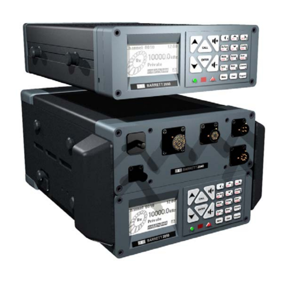
Overview All 2000 series transceivers and receivers are made up of several common building blocks and they are all constructed in the same common chassis. The man-pack consists of a 2050 transceiver mated with a 2040 manpack adaptor which contains the battery management system, battery pack and automatic antenna tuner. -
Page 13: Power Amplifier Pcb
A product detector is used to demodulate all signals, with an envelope detector used to generate AGC control voltage. The noise blanker employs a separate noise pulse receiver to provide raw blanking pulses which are manipulated in the main processor to form effective blanking pulses on the noise blanker gate. There is a great deal of commonality between receive and transmit paths in both the R.F. -
Page 14: Technical Description
Technical description Microprocessor / RF PCB – microprocessor section This PCB is divided into two separated sections. The first section contains the microprocessor, DSP and frequency synthesizer. The synthesiser provides the stable first local oscillator source, the DSP generates and demodulates SELCALL and ALE signals, provides functions such as the audio syllabic mute, additional audio filtering, noise reduction and transmitter power control. -
Page 15: Vco Divider Ratio
VCO divider ratio As mentioned above, the VCO frequency divider U42 normally divides by 10, but sometimes another ratio may be more desirable. This is because the DDFS by its very nature produces spurs at some frequencies. Since the DDFS can produce millions of frequencies, predicting ones which will produce these spurs is not possible. -
Page 16: First Mixer
The RF section has a common RF input and output port and separate audio input for Tx and output for Rx. A double superheterodyne system is used, with a first IF of 45 MHz and second IF at 455 kHz. Three oscillator injection frequencies are used, LO1 at (Carrier frequency + 45 MHz), LO2 at 45.455 MHz and LO3 or the Carrier Insertion Oscillator at 453.4kHz on USB and 456.6kHz on LSB. -
Page 17: 455 Khz If Amplifier
gates are controlled by signals from the microprocessor. These are NOISEGATE 2 on U40 and NOISEGATE1 on the first noise gate U51. The receiver comes with a filter F9 fitted as standard. However, either a narrow filter, F4 or one of two other special purpose filters can be fitted instead. The required filter is selected by analogue bus switches U35 and U36. -
Page 18: Tones
Line output A separate audio output is taken from the DAC (OUT 2) to the line audio output level control U65B, which is of the same type as used for the loud speaker volume control. This is part of a feed back circuit around amplifier U6B. -
Page 19: Transmit Tones
an output increase of only about 3dB. The level at which the onset of compression starts is set by the voltage divider R63 and R108. The compressor output enters the DSP, U2 pin 107 (TX AUDIO) for processing. The transmit audio data emerges from the DSP and is converted to an analogue signal in DAC U63, and emerges from pin 12. -
Page 20: Power Amplifier (Pa) Pcb
Power amplifier (PA) PCB The Power Amplifier raises the power from the exciter to specified output power. It also provides harmonic filtering for the transmitter and low pass filtering in receive mode. Gain control amp The signal from the exciter at a level of approx. -17dBm is fed to a gain controlled amplifier, dual gate MOS FET Q1. -
Page 21: Over-Voltage And Reverse Voltage Protection
Over-voltage and reverse voltage protection Over voltage and reverse voltage protection is incorporated on the PA PCB. The over voltage protection is provided by SCR1 and SCR2. These conduct when the input voltage exceeds about 17 volts. This causes the gate voltage on P channel MOSFETs Q6 and Q7 to pull up to the source voltage, thus turning them off. The power source must be removed for this circuit to be reset. -
Page 22: Control Head - Front Panel
“Enter” button on the front panel. When it detects a primary infrared device, all other processes and button presses (except the power) are suspended. Using the Barrett Programming Software, data packs can be uploaded or downloaded to the transceiver at a baud rate of19200. This process takes between 20 to 45 seconds. -
Page 23: Maintenance
Remove the plastic capstan covers by hand, then using the Barrett tool or a M10 Allen key remove the M10 set screws from the side locks Using the Barrett tool or a M4 Allen key remove the four M4 x 50mm hex head cap screws from the control head front panel, the control head should now be free. - Page 24 Using the Barrett tool or a #2 Philips head screw driver remove the central panel screw:- Grasp both side lock slides and pull out. Using the Barrett tool or an M4 Allen key remove two M4 x 16 cap screws on the rear panel...
- Page 25 Using the Barrett tool or a #2 Philips head screw driver remove the central screw on the back cover Using suitable UNC 4-40 hex nut driver remove the two screw locks from the DB-7 power connector and the two screw locks from the DB-25 auxiliary connector.
- Page 26 Grasp the front panel PCB and draw off from the IDC connector. Remove the central shield plate Grasp the Micro/RF PCB and draw away from the rear panel PCB IDC connector The 2050 is now disassembled. Note:- To reassemble the 2050 transceiver use this process in reverse, making sure ribbon connectors and coaxial connectors are reinstalled and that rubber and foam gaskets that were removed during disassembly are replaced in their original positions to maintain sealing.
-
Page 27: Opening The 2040 For Pcb Access
Opening the 2040 for PCB access Remove the battery cartridge as shown Using an M3 hex driver remove the cap screws as shown Grasp the front panel of the 2040 adaptor and gently pull away from the connectors Using a flat blade screw driver remove the wires from the terminal block to the connector on the battery cartridge housing. - Page 28 Note the location of the cables before disassembly to enable re-assembly The front panel is now free and can be removed Grasp the PCB edge of the automatic antenna tuner PCB and slide out Grasp the PCB edge of the battery charger PCB and gently pull out...
- Page 29 To access components on the battery charger PCB the RF shield must be un-soldered.
-
Page 30: Printed Circuit Board (Pcb) Maintenance
Extensive use of surface mounted components is made on all PCB's in 2000 series transceivers. It is essential that surface mount work stations be used for removal and replacement of these components. -
Page 31: Transmitter Power Amplifier Maintenance Precautions
Make sure test equipment being used has a correct earth on its mains lead. Before and during work on PCB's or handling CMOS devices, discharge static charges, which may build up on a person, by touching a grounded metal surface with both hands. If possible wear a suitably grounded conductive wrist strap. -
Page 32: Fault Diagnosis
The short circuit removes the forward bias cutting off the transistor, so that the voltage across the resistor is considerably reduced. If a fault can be traced to one PCB but no further then consider using Barrett Communications' PCB and module exchange service. -
Page 33: After Power Up The "Barrett Logo" Screen Stays On
(12 to 14V). After power up the “Barrett logo” screen stays on. This indicates that there is no communication between the microprocessor board and the front panel. The Microprocessor board should be exchanged. -
Page 34: Main Microprocessor Faults
Main microprocessor faults Check that the reference oscillator (a DTCXO) Digitally Temperature Compensated XTAL Oscillator is operating at TP5. This should be a CMOS level (3V P-P) signal with a frequency of 22.7275 MHz. VCO faults The VCO should produce an output frequency at TP8 of The signal frequency plus 45MHz. Problems which prevent this include:- Preset divider U42 may be dividing by the wrong ratio. -
Page 35: Expected Signal Levels
Expected signal levels Test point Description of signal Expected levels number 45MHz Filter input See Fig 1 45MHz Filter output See Fig 1 DDFS output, square wave 0-3V (digital) Carrier Insert Oscillator receive (CIO RX). Square wave 0-3V (digital) Master Clock (MCLK), square wave 0-3V (digital) Monitor tones to speaker amp 1 V P-P... - Page 36 Replacement of PA output and driver transistors Under normal operating conditions PA and Driver FETs will last indefinitely. The ALC circuit will fully protect these transistors from incorrect antenna loads. In data mode, if the cooling fan fails for any reason, a high temperature power reducing circuit will protect these devices from overheating.
-
Page 37: Adjustments
Replacing the driver FETs Q4 and Q5 To remove the FETs it is necessary first to remove the PCB from the chassis. Simply undo all of the bolts on the PCB. The PCB will then lift clear. Unsolder the FETs gate and drain leads. This will almost always break the FET. This then leaves the large Source tab in the middle of the FET. -
Page 38: 45Mhz If Filter
45MHz IF Filter A spectrum analyser with tracking generator must be used to align this filter and it should be set with a centre frequency of 45MHz and a span of 50kHz. Solder bridge SP1 and SP2 should be unsoldered, the sweep signal should be injected at TP1 , the spectrum analyser input should be connected to TP2. -
Page 39: Power Amplifier (Pa) Bias Setup
Power Amplifier (PA) bias setup If the PA transistors have been replaced then LK1 and LK2 should be opened. RV2 should be set fully anticlockwise. Power can then be applied to the transceiver and PTT operated but with no audio input. RV2 should be carefully adjusted to obtain 0.67 V on TP09. -
Page 40: Software Options
Barrett 2050 receivers The Barrett 2050R is technically identical to the Barrett 2050 local control transceiver, but has a different PCB fitted in place of the PA PCB containing low pass filters, power relay circuitry and antenna switch components. -
Page 41: Barrett 2040 Manpack Adaptor
Barrett 2040 Manpack Adaptor A standard 2050 transceiver (with local front panel) when plugged into the 2040 Manpack adaptor, converts the 2050 into a 2040 portable Manpack transceiver, complete with automatic antenna tuner. When plugged into the adaptor, the output power is automatically reduced to low power operation. -
Page 42: Internal Charger Pcb
P2 also provides an unbalanced audio input pin. This unbalanced audio is also protected from RF interference by using a choke (L3) and suppression capacitor C12. Coupling capacitor C1 removes any DC component from the audio line before passing the audio to Amplifier U1B. U1B is used as a summing amplifier to combine all of the audio signals into one unbalanced audio signal for the transceiver. -
Page 43: Automatic Antenna Tuner Pcb
Automatic antenna tuner PCB Introduction The Automatic antenna tuner is designed to interface the 2050 transceiver to either a vertical whip or a long wire antenna. The tuner is connected to the base PCB via P2. Tuning Network The whip antenna is resonant at approximately 23MHz. Below resonance the whip presents a capacitive reactance which needs to be tuned out with inductance. -
Page 44: Tuning Algorithm
As soon as power is applied to the tuner PCB, the microcontroller begins sending out a command byte to the 2050 through connector P1. This is to inform the 2050 that it is connected in the Manpack configuration and to setup for portable operation. When the 2050 receives this command byte it replies with an acknowledgement byte and the tuner goes into standby mode waiting for command data from the 2050. -
Page 45: Rear Panel Connectors
Rear panel connectors... -
Page 46: Auxiliary Connector
Auxiliary connector (25 pin female "D" connector on rear panel) Name Description of function Level Ground Ground Rx Data RS-232 data input True RS-232 Tx Data RS-232 data output True RS-232 External Power On For use with ancillary equipment. Low to activate External Speaker External speaker output 0-10V... -
Page 47: Gps Connector
GPS connector NMEA - -12V data input NMEA 0183 format +5 VDC supply max 75mA NMEA + +12V data input NMEA 0183 format Ground Ground 0V 1PPS 1PPS timing pulse TTL level from GPS GPS RX GPS TTL data input Fan connector +13.8VDC Fan control - active low... -
Page 48: Circuit Diagrams And Overlays
Circuit diagrams and overlays 2050 transceiver Click here to view Micro processor / RF schematic and overlay Click here to view PA schematic and overlay Click here to view Front panel PCB schematic and overlay Click here to view Rear Panel PCB schematic and overlay Click here to view Control Head PCB schematic and overlay Click here to view Control Head Transition PCB schematic and overlay 2040 manpack adaptor... -
Page 49: Parts Lists
Parts lists 2050 transceiver - Micro Processor / RF PCB Click here to view Micro processor / RF schematic and overlay PC-2000P01-A2 Micro RF PCB Parts List Barrett Part Designator Description Number Cap 10uF 16v Y5V +80/-20% 1206 NB CP-11710... - Page 50 Cap 100nF 5% 50V 0603 X7R NB CP-11666 Cap 10uF 16v Y5V +80/-20% 1206 NB CP-11710 Cap 100nF 5% 50V 0603 X7R NB CP-11666 Cap 100nF 5% 50V 0603 X7R NB CP-11666 Cap 100nF 5% 50V 0603 X7R NB CP-11666 Cap 100nF 5% 50V 0603 X7R NB CP-11666...
- Page 51 Cap 100nF 5% 50V 0603 X7R NB CP-11666 Cap 100nF 5% 50V 0603 X7R NB CP-11666 Cap 100nF 5% 50V 0603 X7R NB CP-11666 Cap 10nF 5% 50V 0603 X7R NB CP-11667 C100 Cap 10nF 5% 50V 0603 X7R NB CP-11667 C101 Cap 100nF 5% 50V 0603...
- Page 52 C148 Cap 4n7 5% 50V 0603 X7R NB CP-11698 C149 Cap 100nF 5% 50V 0603 X7R NB CP-11666 C150 Cap 100nF 5% 50V 0603 X7R NB CP-11666 C151 Cap 100nF 5% 50V 0603 X7R NB CP-11666 C152 Cap 100nF 5% 50V 0603 X7R NB CP-11666 C153...
- Page 53 C200 Cap 10nF 5% 50V 0603 X7R NB CP-11667 C201 Cap 10nF 5% 50V 0603 X7R NB CP-11667 C202 Cap 10nF 5% 50V 0603 X7R NB CP-11667 C203 Cap 39pF 5% 50V 0603 NPO NB CP-11691 C204 Cap 10nF 5% 50V 0603 X7R NB CP-11667 C205 Cap 10uF 16v Y5V...
- Page 54 C252 Cap 22pF 5% 50V 0603 NPO NB CP-11675 C253 Cap 560pF 5% 50V 0603 X7R NB CP-11699 C254 Cap 150pF 5% 50V 0603 NPO NB CP-11686 C255 Cap 8p2 +/- 0.5pF 50V 0603 NPO NB CP-11695 C256 Cap 68pF 5% 50V 0603 NPO NB CP-11678 C258 Cap 100nF 5% 50V 0603...
- Page 55 Cap Net 1nF 50V NPO 5% NB 0612 CP-11703 Cap Net 1nF 50V NPO 5% NB 0612 CP-11703 Cap Net 10nF 16V X7R 10% NB 0612 CP-11702 Cap Net 10nF 16V X7R 10% NB 0612 CP-11702 CP10 Cap Net 100nF 16V X7R 10% NB 0612 CP-11664 CP11...
- Page 56 Ind 390nH 0805 5% IN-15014 Ind 10uH 1210 IN-03600 Ind 10uH 1210 IN-03600 Ind Coil T1032 IN-15016 Ind 100uH 1210 10% 10R IN-03601 Ind 10uH 1210 IN-03600 Inductor 470uH SMD IN-15004 Inductor 10uH 3DF TOKO IN-15007 Inductor 10uH 3DF TOKO IN-15007 Ind 390nH 0805 5% IN-15014...
- Page 57 Res 100R 5% 0.063W 0603 NB RE-10283 Res 33k 0.063W 5% 0603 NB RE-10318 Res 10k 5% 0.063W 0603 NB RE-10277 Res 10k 5% 0.063W 0603 NB RE-10277 Res 10k 5% 0.063W 0603 NB RE-10277 Res 10k 5% 0.063W 0603 NB RE-10277 Res 10k 5% 0.063W 0603 NB RE-10277...
- Page 58 Res 6k8 0.063W 5% 0603 NB RE-10332 Res 10k 5% 0.063W 0603 NB RE-10277 Res 10k 5% 0.063W 0603 NB RE-10277 Res 10k 5% 0.063W 0603 NB RE-10277 Res 10k 5% 0.063W 0603 NB RE-10277 Res 10k 5% 0.063W 0603 NB RE-10277 Res 100k 5% 0.063W 0603 NB RE-10291...
- Page 59 R108 Res 15k 0.063W 5% 0603 NB RE-10307 R109 Res 22k 0.063W 5% 0603 NB RE-10311 R110 Res 47R 5% 0.063W 0603 NB RE-10281 R111 Res 220R 5% 0.063W 0603 NB RE-10279 R112 Not Fitted R113 Res 47R 5% 0.063W 0603 NB RE-10281 R114 Res 10R 5% 0.063W 0603 NB...
- Page 60 R160 Res 10k 5% 0.063W 0603 NB RE-10277 R161 Res 10R 5% 0.063W 0603 NB RE-10278 R162 Res 100R 5% 0.063W 0603 NB RE-10283 R163 Res 10R 5% 0.063W 0603 NB RE-10278 R164 Res 10R 5% 0.063W 0603 NB RE-10278 R165 Res 220k 5% 0.063W 0603 NB RE-10289...
- Page 61 Res Array 1k 5% 50v 0.063W 1206 4 pack RE-10336 Res Array 1k 5% 50v 0.063W 1206 4 pack RE-10336 Res Array 10k 5% 50v 0.063W 1206 4 pack RE-10303 RP10 Res Array 10k 5% 50v 0.063W 1206 4 pack RE-10303 RP11 Res Array 10k 5% 50v...
- Page 62 IC MC14053BD SMD MOTOROLA Only IC-02720 IC M25P10 SO8W IC-20027 IC LM2940IMP-10 SOT-223 IC-20038 IC OP279GS SO8 IC-20023 IC NC7SB3157P6X MAA06A IC-20035 IC OP279GS SO8 IC-20023 IC MC74AC161D SO16 IC-20016 IC LM2940IMP-10 SOT-223 IC-20038 IC M25P80 SO8W 8MBit Flash IC-20040 IC 24LC512-I/SM SO8W IC-20013 IC CY7C1041CV33-15ZC...
-
Page 63: 2050 Transceiver - Power Amplifier Pcb
2050 transceiver - Power Amplifier PCB Click here to view PA schematic and overlay PC-2000P03-A2 PA PCB Parts List Barrett Part Designator Description Number Cap 560pF 5% 500V 1206 NPO NB CP-00067 Cap 680pF 5% 500V 1206 NPO NB CP-00068... - Page 64 Cap 68pF 5% 500V 1206 NPO NB CP-00057 Cap 150pF 5% 500V 1206 NPO NB CP-00060 Cap 22p 5% 500V Silver mica CP-02151 Cap 12pF 5% 500V 1206 NPO NB CP-00049 Cap 100pF 5% 500V 1206 NPO NB CP-00059 Cap 12pF 5% 500V 1206 NPO NB CP-00049 Cap 18pF 5% 500V 1206...
- Page 65 C103 Cap 10nF 5% 50V 0603 X7R NB CP-11667 C104 Cap 100nF 5% 50V 0603 X7R NB CP-11666 C105 Cap 100nF 5% 50V 0603 X7R NB CP-11666 C106 Cap 10nF 5% 50V 0603 X7R NB CP-11667 C107 Cap 100nF 5% 50V 0603 X7R NB CP-11666 C108...
- Page 66 Di BAV70 SMD DI-03316 Di BAV70 SMD DI-03316 Di BAV70 SMD DI-03316 Di BAV70 SMD DI-03316 Di BAV70 SMD DI-03316 Di BAV70 SMD DI-03316 Di BAV70 SMD DI-03316 Di BAV70 SMD DI-03316 Di S3A 3A DO-214AB SMD DI-03362 Di BAV70 SMD DI-03316 Di BAV70 SMD DI-03316...
- Page 67 Ind 9T L11,12,32 2000 PA IN-15033 Ind 7T L13,14,33 2000 PA IN-15034 Plug 2 pin CN-04101 Board Pins CN-03901 x2 Arrow connectr DAO7W2P500A30 CN-24182 Conn Coax SMB ST PCB F CN-24146 Conn Coax SMB ST PCB F CN-24146 Trans BF1100 SOT143 Dual gate Mosfet Enhance mode TR-02286 Trans BCP56-10 SOT223 TR-02236...
- Page 68 Res 100k 5% 0.063W 0603 NB RE-10291 Res 680R 5% 1/8W 1206 NB RE-00101 Res 12k 0.063W 5% 0603 NB RE-10346 Res 100k 5% 0.063W 0603 NB RE-10291 Res 100k 5% 0.063W 0603 NB RE-10291 Res 10k 5% 0.063W 0603 NB RE-10277 Res 10k 5% 0.063W 0603 NB RE-10277...
-
Page 69: 2050 Transceiver - Front Panel Pcb
2050 Transceiver – Front panel PCB Click here to view Front panel PCB schematic and overlay PC-2000P06-A1 Front Panel PCB Parts List Barrett Part Designator Description Number Plug 5 Pin Double Row Nrml CN-04109 Conn RJ-45 Modular Jack RA PCB Inverted... -
Page 70: 2050 Transceiver - Control Head And Display Transition Pcb's
2050 transceiver - Control head and display transition PCB’s Click here to view Control Head PCB schematic and overlay PC-2000P03-A2 Control Head PCB Parts List Barrett Part Designator Description Number Cap 15pF 5% 50V 0603 NPO NB CP-11687 Cap 15pF 5% 50V 0603 NPO NB... - Page 71 Cap 1uF 5% 16V 0805 Y5V CP-11674 Cap 10uF 16v Y5V +80/-20% 1206 NB CP-11710 Cap 10uF 16v Y5V +80/-20% 1206 NB CP-11710 Cap Net 1nF 50V NPO 5% NB 0612 CP-11703 Cap Net 1nF 50V NPO 5% NB 0612 CP-11703 Cap Net 1nF 50V NPO 5% NB 0612 CP-11703...
- Page 72 Res 1k 5% 0.063W 0603 NB RE-10287 Thermistor 3k PTC 0805 LT73 TH-02560 T/Former F900FCB-1133=P2 TF-30678 IC ST3232BDR SO16 IC-20033 OP279 S08 IC-20023 LCD 2000 SERIES LE-02928 IC LT1616ES6 SOT-23 IC-20008 IC PIC18F452 TQFP44 IC-20012 IC HSDL-7001 SOIC-16 Infrared Encoder/Decoder IC-20039 OP279 S08 IC-20023...
-
Page 73: 2050 Transceiver - Control Head Transition Pcb
2050 transceiver - Control head transition PCB Click here to view Control Head Transition PCB schematic and overlay PC-2000P04-A0 Control Head Transition PCB Parts List Barrett Designator Description Part Number Conn IDC 20W Low Profile Header CN-24155 Conn RJ45 Dual RA Gang Lo Prof Shielded Inverted... -
Page 74: 2040 Manpack Adapter - Front Panel Pcb
2040 Manpack adapter - Front Panel PCB Click here to view Front Panel PCB schematic and overlay PC-2040P02-A1 Front Panel PCB Parts List Barrett Part Designator Description Number Cap 100nF 5% 50V 0603 X7R NB CP-11666 Cap 100nF 5% 50V 0603... - Page 75 Conn Header M 34W Dual ST CN-24153 Plug 5 Pin Double Row Nrml CN-04109 Terminal Strip 3 W CN-03735 Trans 2N7002 LT-1 Fet SOT23 TR-02282 Trans 2N7002 LT-1 Fet SOT23 TR-02282 Trans 2N7002 LT-1 Fet SOT23 TR-02282 Res 22k 0.063W 5% 0603 NB RE-10311 Res 10k 5% 0.063W 0603 NB RE-10277...
-
Page 76: 2040 Manpack Adapter - Base Pcb
2040 Manpack adapter - Base PCB Click here to view Base PCB schematic and overlay PC-2040P01-A1 Base PCB Parts List Designator Description Barrett Part Number Conn D25M ST Wire Wrap CN-24180 Conn Header M 14W Dual ST CN-24190 Conn Header M 40W Dual ST... -
Page 77: 2040 Manpack Adapter - Automatic Antenna Tuner Pcb
2040 Manpack adapter – Automatic antenna tuner PCB Click here to view Automatic antenna tuner PCB schematic and overlay PC-2040P27-A1 ATU PCB Parts List Designator Description Barrett Part Number Cap 6p8 +/- 0.5pF 50V 0603 NPO NB CP-11694 Cap 6p8 +/- 0.5pF 50V... - Page 78 Res 100R 1% 1/8W 1206 NB RE-00117 Res 180R 5% 0.063W 0603 NB RE-new Res 180R 5% 0.063W 0603 NB RE-new Res 180R 5% 0.063W 0603 NB RE-new Res 10k 5% 0.063W 0603 NB RE-10277 Res 10k 5% 0.063W 0603 NB RE-10277 Res 10k 5% 0.063W 0603 NB RE-10277...
-
Page 79: 2040 Manpack Adapter - Internal Charger Pcb
2040 Manpack adapter – Internal charger PCB Click here to view Internal charger PCB schematic and overlay PC-2040P29-A0 Internal Charger PCB Parts List Barrett Part Designator Description Number Cap 1uF 10V +80/-20% 0603 NB CP-11721 Cap 10uF 20% Electro Case B 35V SMD... - Page 80 Ind 22T L2,3,4,5 2040 Charger IN-15036 Ind 22T L2,3,4,5 2040 Charger IN-15036 Conn IDC 40W F RA Dual CN-24194 Conn IDC 36W F RA Dual CN-24193 Trans IRFR5305 TO-252AA TR-02293 Trans BC847 SOT23 NOT PHILIPS TR-02262 Trans 2N7002 LT-1 Fet SOT23 TR-02282 Res 100R 5% 0.063W 0603 NB...
Need help?
Do you have a question about the 2000 Series and is the answer not in the manual?
Questions and answers