
Related Manuals for Asus AAEON GENESYS-KBU6


Summary of Contents for Asus AAEON GENESYS-KBU6
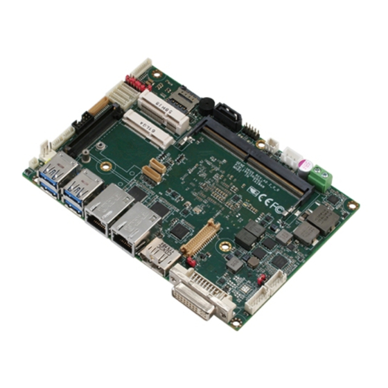
- Page 1 GENESYS-KBU6 3.5” Subcompact Board User’s Manual 1 Last Updated: June 4, 2020...
- Page 2 Copyright Notice This document is copyrighted, 2020. All rights are reserved. The original manufacturer reserves the right to make improvements to the products described in this manual at any time without notice. No part of this manual may be reproduced, copied, translated, or transmitted in any form or by any means without the prior written permission of the original manufacturer.
- Page 3 Acknowledgement All other products’ name or trademarks are properties of their respective owners. Microsoft Windows is a registered trademark of Microsoft Corp. ⚫ Intel, Pentium, Celeron, and Xeon are registered trademarks of Intel Corporation ⚫ Core, Atom are trademarks of Intel Corporation ⚫...
- Page 4 Packing List Before setting up your product, please make sure the following items have been shipped: Item Quantity GENESYS-KBU6 ⚫ If any of these items are missing or damaged, please contact your distributor or sales representative immediately. Preface...
- Page 5 About this Document This User’s Manual contains all the essential information, such as detailed descriptions and explanations on the product’s hardware and software features (if any), its specifications, dimensions, jumper/connector settings/definitions, and driver installation instructions (if any), to facilitate users in setting up their product. Users may refer to the product page on AAEON.com for the latest version of this document.
- Page 6 Safety Precautions Please read the following safety instructions carefully. It is advised that you keep this manual for future references All cautions and warnings on the device should be noted. Make sure the power source matches the power rating of the device. Position the power cord so that people cannot step on it.
- Page 7 If any of the following situations arises, please the contact our service personnel: Damaged power cord or plug Liquid intrusion to the device iii. Exposure to moisture Device is not working as expected or in a manner as described in this manual The device is dropped or damaged Any obvious signs of damage displayed on the device...
- Page 8 FCC Statement This device complies with Part 15 FCC Rules. Operation is subject to the following two conditions: (1) this device may not cause harmful interference, and (2) this device must accept any interference received including interference that may cause undesired operation.
- Page 9 China RoHS Requirements (CN) 产品中有毒有害物质或元素名称及含量 AAEON System QO4-381 Rev.A0 有毒有害物质或元素 部件名称 铅 汞 镉 六价铬 多溴联苯 多溴二苯 醚(PBDE) (Pb) (Hg) (Cd) (Cr(VI)) (PBB) 印刷电路板 × ○ ○ ○ ○ ○ 及其电子组件 外部信号 × ○ ○ ○ ○ ○ 连接器及线材 ○ ○...
- Page 10 China RoHS Requirement (EN) Hazardous and Toxic Materials List AAEON System QO4-381 Rev.A0 Hazardous or Toxic Materials or Elements Component Name PCB and Components Wires & Connectors for Ext.Connections Chassis CPU & RAM HDD Drive LCD Module Optical Drive Touch Control Module Battery This form is prepared in compliance with the provisions of SJ/T 11364.
-
Page 11: Table Of Contents
Table of Contents Chapter 1 - Product Specifications..................1 Specifications ......................2 Chapter 2 – Hardware Information ..................4 Dimensions ....................... 5 Jumpers and Connectors ..................7 List of Jumpers ......................8 2.3.1 Clear CMOS Jumper (JP1) ..............8 2.3.2 mSATA/ Mini-Card Operating VCC Selection (JP5) ...... - Page 12 2.4.15 USB 2.0 Port (CN21) ................23 2.4.16 COM Port 1 (CN25) ................24 2.4.17 COM Port 2 (CN27) ................25 2.4.18 LPC Port (CN29) .................. 27 2.4.19 External Power Input (CN30) ............. 28 Block Diagram ......................28 Hardware Assembly Guide .................. 29 2.6.1 Opening the System ................
- Page 13 3.4.5.4 Serial Port 4 Configuration ..........55 3.4.6 USB Configuration ................56 3.4.7 Digital IO Port Configuration ............57 3.4.8 Power Management ................58 3.4.9 Compatibility Support Module Configuration ......60 Setup submenu: Chipset ..................61 3.5.1 System Agent (SA) Configuration ............ 62 3.5.2 Graphics Configuration ..............
-
Page 14: Chapter 1 - Product Specifications
Chapter 1 Chapter 1 - Product Specifications... -
Page 15: Specifications
Specifications System 7th Generation Intel® Core™ i7/i5/i3/Celeron® Processor SoC 7th Generation Intel® Processor SoC Chipset DDR4 1866/2133, SODIMM x 1 System Memory DVI-D, DP (default) Display Interface DVI-I Intel® i210/i211, 10/100/1000Base-TX, RJ-45 x 2 Ethernet USB 3.2 Gen 1 x 4 (rear I/O) USB 2.0 x 2 (internal option) RS-232 x 1 RS-232/422/485 x 3 (optional) - Page 16 Mechanical Wall mount kit (optional) Mounting 170mm x 44.5mm x 137mm Dimensions (W x H x D) 1.1 kg Gross Weight Environmental 32°F~ 122°F (0°C ~ 50°C), 0.5 m/s airflow Operating Temperature -40°F ~ 176°F (-40°C ~ 81°C) Storage Temperature 0% ~ 90% relative humidity, non-condensing Storage Humidity 2 Grms/ 5 ~ 500Hz/ operation...
-
Page 17: Chapter 2 - Hardware Information
Chapter 2 Chapter 2 – Hardware Information... -
Page 18: Dimensions
Dimensions System Dimensions: Chapter 2 – Hardware Information... - Page 19 Board Component Side Chapter 2 – Hardware Information...
-
Page 20: Jumpers And Connectors
Jumpers and Connectors Chapter 2 – Hardware Information... -
Page 21: List Of Jumpers
List of Jumpers Please refer to the table below for all of the board’s jumpers that you can configure for your application Label Function Clear CMOS Jumper mSATA/Mini-Card Operating VCC Selection Auto Power Button Enable/Disable Selection COM2 Pin8 Function Selection JP10 Front Panel Connector 2.3.1... -
Page 22: Auto Power Button Enable/Disable Selection (Jp7)
2.3.3 Auto Power Button Enable/Disable Selection (JP7) 1 2 3 Disable (Default) Enable Note: When disabled, use power button JP10 (1-2) to power on the system. 2.3.4 COM2 Pin8 Function Selection (JP9) Ring (Default) +12V 2.3.5 Front Panel Connector (JP10) Pin Name Pin Name PWR_BTN-... -
Page 23: List Of Connectors
List of Connectors Please refer to the table below for all of the board’s connectors that you can configure for your application. Label Function Battery DVI-I (Digital and Analog) DP Port SPI Debug Port LAN (RJ-45) Port1 CN10 LAN (RJ-45) Port2 CN11 Mini-Card Slot (Full-Mini Card) CN12... -
Page 24: Battery (Cn1)
2.4.1 Battery (CN1) Pin Name Signal Type Signal level +3.3V 3.3V 2.4.2 DVI-I (Digital and Analog) (CN3) Pin Name Signal Type Signal Level DVI_D2- DVI_D2+ VGA_DDC_CLK VGA_DDC_DAT VGA_VSYNC DVI_D1- DVI_D1+ DVI_D0- DVI_D0+ Chapter 2 – Hardware Information... -
Page 25: Dp Port (Cn5)
Pin Name Signal Type Signal Level DVI_CLK+ DVI_CLK- VGA_RED VGA_GREEN VGA_BLUE VGA_HSYNC 2.4.3 DP Port (CN5) Pin Name Signal Type Signal Level DP_D0+ DIFF DP_D0- DIFF DP_D1+ DIFF DP_D1- DIFF DP_D2+ DIFF DP_D2- DIFF DP_D3+ DIFF DP_D3- DIFF Chapter 2 – Hardware Information... -
Page 26: Bios Debug Port (Cn8)
Pin Name Signal Type Signal Level DP_AUX+ DIFF DP_AUX- DIFF HPLG_DETECT 2.4.4 BIOS Debug Port (CN8) Pin Name Signal Type Signal Level SPI_MISO SPI_CLK +3.3VSB +3.3V SPI_MOSI SPI_CS 2.4.5 LAN (RJ-45) Port1 (CN9) ACT/LINK SPEED Pin Name Signal Type Signal level MDI0+ DIFF MDI0-... -
Page 27: Lan (Rj-45) Port2 (Cn10)
Pin Name Signal Type Signal level MDI2+ DIFF MDI2- DIFF MDI1- DIFF MDI3+ DIFF MDI3- DIFF 2.4.6 LAN (RJ-45) Port2 (CN10) Pin Name Signal Type Signal level MDI0+ DIFF MDI0- DIFF MDI1+ DIFF MDI2+ DIFF MDI2- DIFF MDI1- DIFF MDI3+ DIFF MDI3- DIFF... -
Page 28: Mini-Card Slot (Full-Mini Card) (Cn11)
2.4.7 Mini-Card Slot (Full-Mini Card) (CN11) Pin Name Signal Type Signal level PCIE_WAKE# +3.3VSB +3.3V +1.5V +1.5V PCIE_CLK_REQ# UIM_PWR UIM_DATA PCIE_REF_CLK- DIFF UIM_CLK PCIE_REF_CLK+ DIFF UIM_RST UIM_VPP W_DISABLE# +3.3V PCIE_RST# +3.3V PCIE_RX- DIFF +3.3VSB +3.3V Chapter 2 – Hardware Information... - Page 29 Pin Name Signal Type Signal level PCIE_RX+ DIFF +1.5V +1.5V SMB_CLK +3.3V PCIE_TX- DIFF SMB_DATA +3.3V PCIE_TX+ DIFF USB_D- DIFF USB_D+ DIFF +3.3VSB +3.3V +3.3VSB +3.3V +1.5V +1.5V Chapter 2 – Hardware Information...
-
Page 30: Micro Sim Card Socket (Cn12)
Pin Name Signal Type Signal level +3.3VSB +3.3V 2.4.8 Micro SIM Card Socket (CN12) Pin Name Signal Type Signal Level UIM_PWR UIM_RST UIM_CLK UIM_VPP UIM_DATA 2.4.9 Mini-Card Slot (Half-Mini Card) (CN13) Pin Name Signal Type Signal Level PCIE_WAKE# +3.3VSB +3.3V +1.5V +1.5V PCIE_CLK_REQ#... - Page 31 Pin Name Signal Type Signal Level PCIE_REF_CLK- DIFF PCIE_REF_CLK+ DIFF W_DISABLE# +3.3V PCIE_RST# +3.3V PCIE_RX-/mSATA_RX+ DIFF +3.3VSB +3.3V PCIE_RX+/mSATA_RX- DIFF +1.5V +1.5V SMB_CLK +3.3V PCIE_TX-/mSATA_TX- DIFF SMB_DATA +3.3V PCIE_TX+/mSATA_TX+ DIFF Chapter 2 – Hardware Information...
- Page 32 Pin Name Signal Type Signal Level USB_D- DIFF USB_D+ DIFF +3.3VSB +3.3V +3.3VSB +3.3V +1.5V +1.5V +3.3VSB +3.3V Note: CN13 can be selected for Mini-Card or mSATA by changing BIOS Chapter 2 – Hardware Information...
-
Page 33: Sata Port 1 (Cn14)
2.4.10 SATA Port 1 (CN14) Pin Name Signal Type Signal Level SATA_TX+ DIFF SATA_TX- DIFF SATA_RX- DIFF SATA_RX+ DIFF 2.4.11 +5V Output for SATA HDD (CN15) Pin Name Signal Type Signal Level Chapter 2 – Hardware Information... -
Page 34: Usb 3.0 Ports (Cn18)
2.4.12 USB 3.0 Ports (CN18) Pin Name Signal Type Signal Level +5VSB USB_D- DIFF USB_D+ DIFF USB_SSRX− DIFF USB_SSRX+ DIFF USB_SSTX− DIFF USB_SSTX+ DIFF +5VSB USB_D- DIFF USB_D+ DIFF USB_SSRX− DIFF USB_SSRX+ DIFF USB_SSTX− DIFF USB_SSTX+ DIFF Chapter 2 – Hardware Information... -
Page 35: Usb 3.0 Ports (Cn19)
2.4.13 USB 3.0 Ports (CN19) Pin Name Signal Type Signal Level +5VSB USB_D- DIFF USB_D+ DIFF USB_SSRX− DIFF USB_SSRX+ DIFF USB_SSTX− DIFF USB_SSTX+ DIFF +5VSB USB_D- DIFF USB_D+ DIFF USB_SSRX− DIFF USB_SSRX+ DIFF USB_SSTX− DIFF USB_SSTX+ DIFF Chapter 2 – Hardware Information... -
Page 36: Usb 2.0 Port (Cn20)
2.4.14 USB 2.0 Port (CN20) Pin Name Signal Type Signal Level +5VSB USB_D- DIFF USB_D+ DIFF 2.4.15 USB 2.0 Port (CN21) Pin Name Signal Type Signal Level +5VSB USB_D- DIFF USB_D+ DIFF G ND Chapter 2 – Hardware Information... -
Page 37: Com Port 1 (Cn25)
2.4.16 COM Port 1 (CN25) Pin Name Signal Type Signal Level ±9V ±9V ±9V Chapter 2 – Hardware Information... -
Page 38: Com Port 2 (Cn27)
2.4.17 COM Port 2 (CN27) RS-232 Pin Name Signal Type Signal Level ±5V ±5V ±5V RI/+5V/+12V IN/ PWR +5V/+12V RS-485 Pin Name Signal Type Signal Level RS485_D- ±5V Chapter 2 – Hardware Information... - Page 39 Pin Name Signal Type Signal Level RS485_D+ ±5V NC/+5V/+12V +5V/+12V RS-422 Pin Name Signal Type Signal Level RS422_TX- ±5V RS422_TX+ ±5V RS422_RX+ RS422_RX- NC/+5V/+12V +5V/+12V Note 1: COM2 RS-232/422/485 can be set by BIOS setting. Default is RS-232. Note 2: Pin 8 function can be set by JP9. Chapter 2 –...
-
Page 40: Lpc Port (Cn29)
2.4.18 LPC Port (CN29) Pin Name Signal Type Signal Level LAD0 +3.3V LAD1 +3.3V LAD2 +3.3V LAD3 +3.3V +3.3V +3.3V LFRAME# LRESET# +3.3V LCLK LDRQ0 LDRQ1 SERIRQ +3.3V Chapter 2 – Hardware Information... -
Page 41: External Power Input (Cn30)
2.4.19 External Power Input (CN30) Pin Name Signal Type Signal Level +12V +9~+36V (or +12V) Block Diagram Chapter 2 – Hardware Information... -
Page 42: Hardware Assembly Guide
Hardware Assembly Guide This section details the steps to installing your device’s drive (HDD or SSD), RAM module, and Mini-Card modules (Half-Sized and Full-Sized mPCIe/mSATA cards). Be sure to read instructions before assembly and ensure that you have the required parts before proceeding. -
Page 43: Opening The System
2.6.1 Opening the System Step 1: Remove the four screws from the front panel (with AAEON Logo) of the system. Then remove the two screws connecting the bottom panel to the rear panel. Step 3: Slide the panel back slightly, then lift open from the rear. Note: There are several wires and cables connected to the front panel, be careful when lifting the panel. -
Page 44: Ram Module Installation
2.6.2 RAM Module Installation Step 1: Install the memory RAM module. Insert at an angle (~30°) and then gently press down until it is secured in place (you will hear a click). Step 2: Take the small thermal pad and remove the clear backing. Stick the pad to the drive mounting bracket. -
Page 45: Mini-Card Installation
2.6.3 Mini-Card Installation Step 1: Remove both half-size and full-size mSATA mounting screws from the board. Step 2: Insert your half-size Mini-Card (mSATA) module into the first mSATA slot. Insert at an angle (~30°) then press down gently and secure with screw. Step 3: Insert your full-size Mini-Card (mSATA) module into the second slot. -
Page 46: Storage Drive Installation
2.6.4 Storage Drive Installation Step 1: Remove the four screws from the bottom panel securing the drive mounting bracket, and remove the bracket from the system. Connect the SATA and SATA Power cables to the 2.5” storage drive. Note: Do not connect the cables to the board at this time. - Page 47 Step 3: Remove the clear backing from the large thermal pad and place onto the drive, gently pushing down to adhere to the drive. Then, remove the backing from the exposed side. Step 4: Line up the large hole on the drive bracket with the VESA mount post on the bottom panel.
-
Page 48: Reattach Panel
Step 6: For cable management, use a zip tie to attach the SATA and SATA Power cables to the loop on the top panel as shown. Be sure to cut any excess from the zip tie. 2.6.5 Reattach Panel Step 1: Being careful of cables, slide the tab on the bottom panel under the rear panel, lining up the holes. -
Page 49: Install Wall Mount Brackets
2.6.6 Install Wall Mount Brackets For this task, you need two wall mount brackets and four steel screws included in the wall mount kit. Line up the brackets with the four open holes on the bottom panel of the system as shown, then secure brackets with the four screws. -
Page 50: Vesa Mounting Kit
2.6.7 VESA Mounting Kit For this task, you need the VESA bracket and two steel screws included in the VESA mount kit. Insert screws into the two empty holes on the bottom panel of the system as shown. The system can now be attached to the VESA bracket. Note: This image is for illustrative purposes. -
Page 51: Chapter 3 - Ami Bios Setup
Chapter 3 Chapter 3 - AMI BIOS Setup... -
Page 52: System Test And Initialization
System Test and Initialization The board uses certain routines to perform testing and initialization. If an error, fatal or non-fatal, is encountered, a few short beeps or an error message will be outputted. The board can usually continue the boot up sequence with non-fatal errors. The system configuration verification routines check the current system configuration against the values stored in the CMOS memory. -
Page 53: Ami Bios Setup
AMI BIOS Setup The AMI BIOS ROM has a pre-installed Setup program that allows users to modify basic system configurations, which is stored in the battery-backed CMOS RAM and BIOS NVRAM so that the information is retained when the power is turned off. To enter BIOS Setup, press <Del>... -
Page 54: Setup Submenu: Main
Setup submenu: Main Chapter 3 – AMI BIOS Setup... -
Page 55: Setup Submenu: Advanced
Setup submenu: Advanced Chapter 3 – AMI BIOS Setup... -
Page 56: Cpu Configuration
3.4.1 CPU Configuration Options Summary Hyper-Threading Disabled Enabled Optimal Default, Failsafe Default Enabled for Windows XP and Linux (OS optimized for Hyper-Threading Technology) and Disabled for other OS (OS not optimized for Hyper-Threading Technology). Active Processor Cores Optimal Default, Failsafe Default Number of cores to enable in each processor package. - Page 57 Options Summary Intel(R) SpeedStep(tm) Disabled Enabled Optimal Default, Failsafe Default Allows more than two frequency ranges to be supported. Turbo Mode Disabled Enabled Optimal Default, Failsafe Default Enable/Disable processor Turbo Mode (requires EMTTM enabled too). AUTO means enabled, unless max turbo ratio is bigger than 16 - SKL A0 W/A Chapter 3 –...
-
Page 58: Trusted Computing
3.4.2 Trusted Computing Options Summary Security Device Disable Support Enable Optimal Default, Failsafe Default Enables or Disables BIOS support for security device. O.S. will not show Security Device. TCG EFI protocol and INT1A interface will not be available. SHA-1 PCR Bank Disable Enable Optimal Default, Failsafe Default... - Page 59 Options Summary Platform Hierarchy Disable Enable Optimal Default, Failsafe Default Enable or Disable Platform Hierarchy Storage Hierarchy Disable Enable Optimal Default, Failsafe Default Enable or Disable Storage Hierarchy Endorsement Disable Hierarchy Enable Optimal Default, Failsafe Default Enable or Disable Endorsement Hierarchy TPM2.0 UEFI Spec TCG_2 Optimal Default, Failsafe Default...
-
Page 60: Sata Configuration
3.4.3 SATA Configuration Options Summary SATA Controller(s) Enabled Optimal Default, Failsafe Default Disabled Enable or disable SATA Device. SATA Mode AHCI Mode Optimal Default, Failsafe Default RAID Mode Determines how SATA controller(s) operate. Port 0 Disabled Enabled Optimal Default, Failsafe Default Enable or Disable SATA Port. -
Page 61: Hardware Monitor
3.4.4 Hardware Monitor Options Summary Smart Fan Enabled Enable or Disable Smart Fan Disabled FAN1 Output Mode Output PWM mode (push pull) Linear Fan Application Optimal Default, Failsafe Default Output PWM mode (open drain) Output PWM mode (push pull) to control 4-wire fans. Linear fan application circuit to control 3-wire fan speed by fan’s power terminal. -
Page 62: Smart Fan Mode Configuration
3.4.4.1 Smart Fan Mode Configuration Fan Mode: [Auto Duty] Options Summary Fan Mode Manual Duty Auto Duty Optimal Default, Failsafe Default Smart Fan Mode Select Duty Cycle Auto fan speed control. Fan speed will follow different temperature by different duty cycle 60-100 Temperature Chapter 3 –... - Page 63 Fan Mode: [Manual Duty] Options Summary Manual Duty Mode Optimal Default, Failsafe Default Manual mode fan control, user can write expected duty cycle (PWM fan type) 60-100 Chapter 3 – AMI BIOS Setup...
-
Page 64: Sio Configuration
3.4.5 SIO Configuration Chapter 3 – AMI BIOS Setup... -
Page 65: Serial Port 1 Configuration
3.4.5.1 Serial Port 1 Configuration Options Summary Use This Device Disabled Enabled Optimal Default, Failsafe Default Enable or Disable Serial Port (COM) Possible: Use Automatic Settings Optimal Default, Failsafe Default IO=3F8; IRQ=4; IO=2F8; IRQ=3; Select an optimal setting for IO device Chapter 3 –... -
Page 66: Serial Port 2 Configuration
3.4.5.2 Serial Port 2 Configuration Options Summary Use This Device Disabled Enabled Optimal Default, Failsafe Default Enable or Disable Serial Port (COM) Possible: Use Automatic Settings Optimal Default, Failsafe Default IO=2F8; IRQ=3; IO=3F8; IRQ=4; Mode: RS232 UART RS232, 422, 485 selection RS422 RS485 Select an optimal setting for IO device... -
Page 67: Serial Port 3 Configuration
3.4.5.3 Serial Port 3 Configuration Options Summary Use This Device Disabled Enabled Optimal Default, Failsafe Default Enable or Disable Serial Port (COM) Possible: Use Automatic Settings Optimal Default, Failsafe Default IO=3E8; IRQ=11; IO=2E8; IRQ=11; Mode: RS232 UART RS232, 422, 485 selection RS422 RS485 Select an optimal setting for IO device... -
Page 68: Serial Port 4 Configuration
3.4.5.4 Serial Port 4 Configuration Options Summary Use This Device Disabled Enabled Optimal Default, Failsafe Default Enable or Disable Serial Port (COM) Possible: Use Automatic Settings Optimal Default, Failsafe Default IO=2E8; IRQ=11; IO=3E8; IRQ=11; Mode: RS232 UART RS232, 422, 485 selection RS422 RS485 Select an optimal setting for IO device... -
Page 69: Usb Configuration
3.4.6 USB Configuration Options Summary Legacy USB Support Enabled Optimal Default, Failsafe Default Disabled Auto Enables BIOS Support for Legacy USB Support. When enabled, USB can be functional in legacy environment like DOS. AUTO option disables legacy support if no USB devices are connected Chapter 3 –... -
Page 70: Digital Io Port Configuration
3.4.7 Digital IO Port Configuration Options Summary DIO Port* Output Input Set DIO as Input or Output Output Level High Optimal Default, Failsafe Default Set output level when DIO pin is output Chapter 3 – AMI BIOS Setup... -
Page 71: Power Management
3.4.8 Power Management Options Summary Power Mode ATX Type Optimal Default, Failsafe Default AT Type Select system power mode. Power Saving(ERP) Disabled Optimal Default, Failsafe Default Control Enabled Configure power mode for power saving function. Restore on Power Last State Optimal Default, Failsafe Default Loss Power On... - Page 72 Options Summary Resume from Disabled LAN/RI Enabled Optimal Default, Failsafe Default Enable/Disable Resume from LAN/RI Chapter 3 – AMI BIOS Setup...
-
Page 73: Compatibility Support Module Configuration
3.4.9 Compatibility Support Module Configuration Options Summary Boot option filter UEFI and Legacy Optimal Default, Failsafe Default Legacy only UEFI only This option controls Legacy/UEFI ROMs priority Storage Do not launch UEFI Legacy Optimal Default, Failsafe Default Controls the execution of UEFI and Legacy Storage OpROM Video Do not launch UEFI... -
Page 74: Setup Submenu: Chipset
Setup submenu: Chipset Chapter 3 – AMI BIOS Setup... -
Page 75: System Agent (Sa) Configuration
3.5.1 System Agent (SA) Configuration Options Summary Max TOLUD Dynamic Optimal Default, Failsafe Default 1 GB 1.25 GB 1.5 GB 1.75 GB 2 GB 2.25 GB 2.5 GB 2.75 GB 3 GB 3.25 GB 3.5 GB Maximum Value of TOLUD Dynamic assignment would adjust TOLUD automatically based on largest MMIO length of installed graphic controller. -
Page 76: Graphics Configuration
3.5.2 Graphics Configuration Options Summary Primary IGFX Boot VBIOS Default Optimal Default, Failsafe Default Display CRT/DP LVDS Select the Video Device which will be activated during POST. This has no effect if external graphic present. Secondary boot display selection will appear based on your selection. Secondary IGFX Boot Disabled Optimal Default, Failsafe Default... -
Page 77: Lvds Panel Configuration
3.5.3 LVDS Panel Configuration Options Summary LVDS Disabled Enabled Optimal Default, Failsafe Default Enable/Disabled this panel. LVDS Panel Type 640x480,18bit,60Hz 800x480,18bit,60Hz 800x600,18bit,60Hz 1024x600,18bit,60Hz 1024x768,18bit,60Hz Optimal Default, Failsafe Default 1024x768,24bit,60Hz 1280x768,24bit,60Hz 1280x1024,48bit,60Hz 1366x768,24bit,60Hz 1440x900,48bit,60Hz 1600x1200,48bit,60Hz 1920x1080,48bit,60Hz 1920x1200,48bit,60Hz Chapter 3 – AMI BIOS Setup... - Page 78 Options Summary Select LCD panel used by Internal Graphics Device by selecting the appropriate setup item. Color Depth 18-bit Optimal Default, Failsafe Default 24-bit 36-bit 48-bit Select panel type Backlight Type Normal Optimal Default, Failsafe Default Inverted Select backlight control signal type Backlight Level Optimal Default, Failsafe Default 100%...
-
Page 79: Pch-Io Configuration
3.5.4 PCH-IO Configuration Options Summary HD Audio Disabled Enabled Optimal Default, Failsafe Default Control Detection of the HD-Audio device. Disabled = HDA will be unconditionally disabled Enabled = HDA will be unconditionally enabled Auto = HDA will be enabled if present, disabled otherwise. PCI Express Root Enabled Optimal Default, Failsafe Default... -
Page 80: Security
Security Change User/Administrator Password You can set an Administrator Password or User Password. An Administrator Password must be set before you can set a User Password. The password will be required during boot up, or when the user enters the Setup utility. A User Password does not provide access to many of the features in the Setup utility. -
Page 81: Setup Submenu: Boot
Setup Submenu: Boot Options Summary Quiet Boot Disabled Enabled Optimal Default, Failsafe Default Enable or Disable showing boot logo. Launch PXE OpROM Disabled Optimal Default, Failsafe Default Enabled Controls the execution of UEFI and Legacy PXE OpROm Chapter 3 – AMI BIOS Setup... -
Page 82: Bbs Priorities
3.7.1 BBS Priorities Chapter 3 – AMI BIOS Setup... -
Page 83: Setup Submenu: Save & Exit
Setup Submenu: Save & Exit Chapter 3 – AMI BIOS Setup... -
Page 84: Chapter 4 - Drivers Installation
Chapter 4 Chapter 4 – Drivers Installation... -
Page 85: Drivers Download And Installation
Drivers Download and Installation Drivers for the GENESYS-KBU6 can be downloaded from the product page on the AAEON website by following this link: https://www.aaeon.com/en/p/3-and-half-inches-subcompact-boards-GENESYS-kbu6 Download the driver(s) you need and follow the steps below to install them. Step 1 – Install Chipset Drivers Open the Step1 - Chipset folder followed by SetupChipset.exe Follow the instructions Drivers will be installed automatically... - Page 86 Step 5 – Install PenMount Touch 6000 Driver Open the Step 5 - PenMount Touch 6000 folder followed by Setup.exe Follow the instructions Drivers will be installed automatically Step 6 – Install Serial Port Drivers (Optional) Click on the Step 6 - Serial Port Driver (Optional) folder followed by setup.exe Follow the instructions Drivers will be installed automatically...
-
Page 87: Note On Ehci
Note on EHCI With the EHCI controller no longer available on the 6 Gen Intel ® Core™ platforms or later, it is recommended to install Windows 7 through a SATA bus, i.e. SATA DVD-ROM, or patch the EHCI driver onto an installation media for Windows 7. More information can be found in the links below. -
Page 88: Appendix A - I/O Information
Appendix A Appendix A - I/O Information... -
Page 89: I/O Address Map
I/O Address Map Appendix A – I/O Information... - Page 90 Appendix A – I/O Information...
-
Page 91: A.2 Memory Address Map
A.2 Memory Address Map Appendix A – I/O Information... - Page 92 Appendix A – I/O Information...
-
Page 93: A.3 Irq Mapping Chart
A.3 IRQ Mapping Chart Appendix A – I/O Information... - Page 94 Appendix A – I/O Information...
-
Page 95: Appendix B - Electrical Specifications For I/O Ports
Appendix B Appendix B – Electrical Specifications for I/O Ports... -
Page 96: Electrical Specifications For I/O Ports
Electrical Specifications for I/O Ports I/O Port Reference Signal Name Rate Output DVI Port +5V/1A (reserved) DP port +3.3V +3.3V/1A Mini-Card Slot (Full-Mini +3.3VSB +3.3V/1.1A CN11 Card) +1.5V +1.5V/0.375A Mini-Card Slot (Half-Mini +3.3VSB +3.3V/1.1A CN13 Card) +1.5V +1.5V/0.375A +5V Output for SATA HDD CN15 +5V/1A USB 3.0 Ports... -
Page 97: Appendix C - List Of Mating Connectors And Cables
Appendix C Appendix C – List of Mating Connectors and Cables... -
Page 98: Connector And Cable Specifications
Connector and Cable Specifications Mating Connector Connector Available Function Cable P/N Label Cable Vendor Model no. External RTC Battery Molex 51021-0200 175011901C Connector Cable SATA CN14 Molex 88750-5318 SATA Cable 170X000085 Connector +5Vout 2 Pins for CN15 PHR-2 1702150155 Connector HDD Power USB Port USB Wafer...