Table of Contents
Advertisement
Quick Links
Service Manual
CONTENTS
Specification .......................................................................... 1
Laser beam safety precaution ............................................... 2
Mechanism replacement ....................................................... 2
Trouble shooting ................................................................... 5
Service mode ........................................................................ 9
How to load software for MPEG P.W.Board ......................... 12
Tuner Adjustment .................................................................. 13
Exploded View (Cabinet & Chassis) ..................................... 14
Parts List ............................................................................... 15
Exploded View (DVD Mechanism) ........................................ 20
Parts List ............................................................................... 20
IC Block Diagram & Description ............................................ 21
Block diagram ....................................................................... 36
Schematic Diagram (DVD) .................................................... 38
All manuals and user guides at all-guides.com
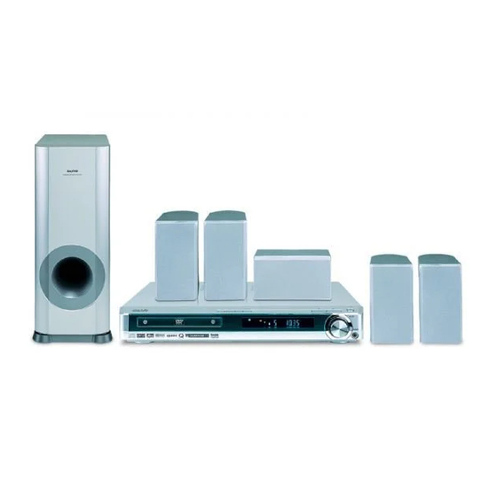
DVD Home Theater System
FILE NO.
DC-TS760
PRODUCT CODE No.
129 656 05
Schematic Diagram (MPEG) ................................................. 40
Schematic Diagram (AMP ) ................................................... 42
Wiring Diagram (MAIN A side) ............................................ 44
(MAIN A side Top Left) ....................................................... 46
(MAIN A side Bottom Left) .................................................. 48
(MAIN A side Top Right) ..................................................... 50
(MAIN A side Bottom Right) ................................................ 52
(B side) ................................................................................ 54
Schematic Diagram (FRONT , TUNER) ................................ 56
Wiring Diagram (FRONT , SW1 BUTTON, SW2 BUTTON,
MECHA SW and MECHA IF) ............................................... 58
Wiring Diagram (TUNER and COMPONENT) .................... 60
Wiring Diagram (POWER SUPPLY) ................................... 62
Wiring Connection ................................................................. rear
REFERENCE No.
(AU)
SM
5810384
Advertisement
Table of Contents

Related Manuals for Sanyo DC-TS760


Summary of Contents for Sanyo DC-TS760
-
Page 1: Table Of Contents
All manuals and user guides at all-guides.com FILE NO. Service Manual DVD Home Theater System DC-TS760 (AU) CONTENTS PRODUCT CODE No. 129 656 05 Schematic Diagram (MPEG) ..........40 Specification ................1 Schematic Diagram (AMP ) ........... 42 Laser beam safety precaution ..........2 Wiring Diagram (MAIN A side) .......... -
Page 2: Specification
Laser: Semiconductor laser, wavelength: 650/790 nm IMPORTANT INFORMATION Laser output (Continuous wave max.): Because its products are subject to continuous improvement, SANYO 1 mW (DVD) reserves the right to modify product designs and specifications without 0.5 mW (CD) notice and without incurring any obligation. -
Page 3: Laser Beam Safety Precaution
All manuals and user guides at all-guides.com DVD MECHANISM REPLACEMENT 1. Cautionary instructions in handling the assy (Connectors) (Safety instructions) Do not connect or disconnect while power is on. Optical pickup Connecting or disconnecting signal wires or the main power cord The laser beam used in the pickup is classified as "class 2". -
Page 4: Mechanism Replacement
All manuals and user guides at all-guides.com MECHANISM REPLACEMENT 1. How to Remove DVD Mechanism Side of DVD mechanism First, it is necessary to remove Escutcheon. Front Rear Cylindrical thing How to remove Escutcheon. An eject button is pushed and a tray is taken out. Please remove Escutcheon, as shown in the left figure 2 . - Page 5 All manuals and user guides at all-guides.com MECHANISM REPLACEMENT 5. Base mechanism mounting parts. G-FLOIL GREASE SY-31S G-FLOIL GREASE SY-31S G-FLOIL GREASE MEN-223R G-FLOIL GREASE MEN-223R G-FLOIL GREASE SY-31S G-FLOIL GREASE MEN-223R G-FLOIL GREASE SY-31S G-FLOIL GREASE MEN-223R : Clean the groove by alcohol well. Apply screw lock 7.
-
Page 6: Trouble Shooting
All manuals and user guides at all-guides.com TROUBLE SHOOTING VIDEO COMPOSITE OUT ; OK TUNER OUTPUT ; OK VIDEO 1,2 OUTPUT ; OK DVD/CD OUTPUT ; NG LOADER CHANGE LOADER CHANGE DAC5V LINE CONFIRM 3.3V,DAC5V 3.3V LINE CONFIRM CONFIRM IC412 PERIPHERAL CIRCUIT CN870 Pin1,15,18 CONFIRM (IC411,IC410 etc) IC870 Pin17,19,21,23,25,27... - Page 7 All manuals and user guides at all-guides.com TROUBLE SHOOTING AC CORD PLUG IC430 SYSCON IC241 TU-PLL SYS-CLK X4300 DS601 IC430,IC601 +5V POWER ONLY FUNCTION DVD-MPU IC451 IC800 & & VOLUME MPEG IC601 IC818 VFD-DRV FLASH IC430 RESET IC870 IC821 6CH-DAC SDROM IC801 EEPROM...
- Page 8 All manuals and user guides at all-guides.com TROUBLE SHOOTING NO COLOR or ABNORMAL X8230 CRYSTAL RESONATOR 27MHz CHANGE IC800 OUTPUT LINE CONFIRM IC800 Pin 169~173 PERIPHERAL VIDEO OUTPUT CONFIRM NORMAL OK? LPF CONFIRM IC800 NG FLOATING CONFIRM IC800 NG TUNER OUTPUT ; NG VIDEO 1,2 OUTPUT ;...
-
Page 9: Service Mode
All manuals and user guides at all-guides.com SERVICE MODE A. Market / Region SETUP In the initial condition for this model, Market and Region information are undefined. In the following cases, be sure to set up Market/Region. 1. When updating the system using CD-R (Part code : 0PRADF9655--AA). - Page 10 All manuals and user guides at all-guides.com SERVICE MODE C. Setup Procedures 1. Displaying SERVICE MODE screen Region M a r k e t Display Service Mode screen following the instructions "How to BackendVersion S21225A1 enter Service Mode" above. LoaderVersion 55 50 05 Value 2.
- Page 11 55 50 05 Value Backend version S 21225 A 1 Brand (S : SANYO , F : FISHER) Version ( 2 0 0 2 , 12 , 25) Sub Version (A,B,..Z) Region ( 0 : Region undefined 1 ~ 6 : Region defined ) (Reference figure) 6.2 Power OFF.
-
Page 12: How To Load Software For Mpeg P.w.board
All manuals and user guides at all-guides.com SERVICE MODE D. IMPORTANT NOTE 1. Once the "Market/Region" settings are written into EEPROM (IC818) on the DVD substrate, they cannot be reset. (However, updating the system using CD-R enables you to make new settings.) 2. -
Page 13: Tuner Adjustment
All manuals and user guides at all-guides.com TUNER ADJUSTMENTS • Use a plastic screw driver for adjustments. SG RF Level : 75Ω open Voltage dBµV Antenna : 75Ω unbalanced Direct, Modulation : 1 kHz Dev. : ±22.5kHz(MONO) , ±22.5kHz(STEREO) , ±6.75kHz(PILOT) Output Level : about 100mV at TP13,TP14,TP15 L2102 L2101... -
Page 14: Exploded View (Cabinet & Chassis)
All manuals and user guides at all-guides.com EXPLODED VIEW (CABINET & CHASSIS) - 14 -... -
Page 15: Parts List
All manuals and user guides at all-guides.com PARTS LIST PRODUCT SAFETY NOTICE EACH PRECAUTION IN THIS MANUAL SHOULD BE FOLLOWED DURING SERVICING. COMPONENTS IDENTIFIED WITH THE IEC SYMBOL IN THE PARTS LIST AND THE SCHEMATIC DIAGRAM DESIGNATED COMPONENTS IN WHICH SAFETY AND ! ! ! PERFORMANCE CAN BE OF SPECIAL SIGNIFICANCE. - Page 16 All manuals and user guides at all-guides.com PARTS LIST REF.NO. PART NO. DESCRIPTION SW2,BUTTON P.W.BOARD ASSY C4102 403 325 0302 ELECT 2200U M 25V C4103 403 325 0302 ELECT 2200U M 25V REF.NO. PART NO. DESCRIPTION C4108 403 325 9701 ELECT 4700U M 25V 614 325 6205 ASSY,PWB,SW2,BUTTON C4109 403 325 2306 ELECT 4700U M 35V...
- Page 17 All manuals and user guides at all-guides.com PARTS LIST REF.NO. PART NO. DESCRIPTION REF.NO. PART NO. DESCRIPTION D4300 407 012 4406 DIODE 1SS133 L4750 645 057 4405 INDUCTOR,0.7U D4301 407 012 4406 DIODE 1SS133 645 053 7493 INDUCTOR,0.7U D4302 407 012 4406 DIODE 1SS133 L4751 645 057 4405 INDUCTOR,0.7U D4303...
- Page 18 All manuals and user guides at all-guides.com PARTS LIST REF.NO. PART NO. DESCRIPTION 405 011 1006 TR 2SC1623-L6 TUNER P.W.BOARD ASSY Q4580 405 146 2107 TR KTC3875-Y REF.NO. PART NO. DESCRIPTION 405 146 2206 TR KTC3875-GR 614 326 3838 ASSY,PWB,TUNER(Only initial) 405 014 4509 TR 2SC2412K-R B2101 645 006 3602 INDUCTOR,1.1UH...
- Page 19 All manuals and user guides at all-guides.com PARTS LIST REF.NO. PART NO. DESCRIPTION 405 004 4601 TR 2SA608-F-SPA 405 004 5103 TR 2SA608-G-SPA 405 006 1806 TR 2SA933S-R 405 006 1905 TR 2SA933S-S Q4006 405 138 6502 TR KTB1366Y Q4007 405 143 6504 TR KTA1267-GR 405 004 4601 TR 2SA608-F-SPA 405 004 5103 TR 2SA608-G-SPA...
-
Page 20: Exploded View (Dvd Mechanism)
All manuals and user guides at all-guides.com EXPLODED VIEW (DVD MECHANISM) DM17 DM17 DM02 DM18 DM18 DM20 DM04 DM26 DM03 DM05 DM27 DM21 DM28 DM06 DM29 DM22 DM07 DM30 DM19 DM23 DM41 DM32 DM24 DM36 DM25 DM33 DM08 DM17 DM18 DM34 DM17 DM18... -
Page 21: Ic Block Diagram & Description
All manuals and user guides at all-guides.com IC BLOCK DIAGRAM & DESCRIPTION FL601 Fluorecent Tube Note FN ; Filament pin nG ; Grid pin Pn ; Anode pin NP ; No Pin NX ; No Extended pin PIN NO. 35 34 33 32 31 30 29 28 27 26 25 24 23 22 21 20 19 18 17 16 15 14 13 12 11 10 9 8 7 6 5 4 3 2 CONNECTION F2 F2 NP P1 P2 P3 P4 P5 P6 P7 P8 P9 P10 P11 P12 P13 P14 P15 P16 P17 P18 P19 NX 9G 8G 7G 6G 5G 4G 3G 2G 1G NP F1 F1... - Page 22 All manuals and user guides at all-guides.com IC BLOCK DIAGRAM & DESCRIPTION IC100 LA9703WL-MPB (DVD Player Fronted Processor) Functions Functions Terminal No. Symbole Terminal No Symbole Customer OP amp. + input EQL boost adjusting Power supply (For DPD) EQL I/O control Pickup signal input FE balance adjusting PDRF...
- Page 23 All manuals and user guides at all-guides.com IC BLOCK DIAGRAM & DESCRIPTION IC130 LC78663NRW (DVD/CD Signal Processing) Block Pin Name Supplementation Block Pin Name Supplementation Servo A/D AD1 Microcom- DVSS Digital GND Servo A/D AD0 puter I/F HDAT1 Data bus 1 Servo A/D JV HDAT2 Data bus 2...
- Page 24 All manuals and user guides at all-guides.com IC BLOCK DIAGRAM & DESCRIPTION IC130 LC78663W-D(DVD/CD Signal Processing) Block Pin name Supplementation Block Pin name Supplementation AV data AVREQI AV data requirement flag input System X16MIO External 16MHz output AVACKO AV data read strobe output TEST2 Test input 2 AVDACK...
- Page 25 All manuals and user guides at all-guides.com IC BLOCK DIAGRAM & DESCRIPTION IC131 M11L416256(256K x 16 DRAM) IC231 LA1844ML(AM/FM-IF/MPX) DATA-IN BUFFER CONTROL LOGIC CASL IO15 CASH CLOCK GENERATOR RF.AMP DATA-OUT PILOT DECODER BUFFER BUFF ANTI-BIRDIE CANCEL COLUMN COLUMN DECODER ADDRESS BUFFER P-DET STEREO...
- Page 26 All manuals and user guides at all-guides.com IC BLOCK DIAGRAM & DESCRIPTION IC161 BA10358(Operational Amplifier) IC410,411 PQ1CG21H2RZ(Chopper Regulator) Constant- OUT1 ON/OFF voltage Circuit circuit ON/OFF -IN1 OUT2 Soft start Overcurrent +IN1 -IN2 detection circuit Oadj +IN2 Overheat detection circuit IC453,455 KTC801U-Y(Switching Transistor) IC450,460 NJM4558(Operational Amplifier) A: OUT B: OUT...
- Page 27 All manuals and user guides at all-guides.com IC BLOCK DIAGRAM & DESCRIPTION IC430 M38507M8(Micro Computer) RESET Sub- Sub- clock clock input output Ciock generating C P U circuit R A M Timer 1(8) R O N Prescaler 12(8) Timer 2(8) Prescaler X(8) Timer X(8) CNTR...
- Page 28 All manuals and user guides at all-guides.com IC BLOCK DIAGRAM & DESCRIPTION IC801 AT24C02N-10SI(EEPROM) START STOP LOGIC SERIAL H,V. PUMP/TIMING CONTROL LOGIC LOAD COMP DATA RECOVERY DEVICE ADDRESS LOAD COMPARATOR DATA WORD E PROM ADDR/COUNTER SERIAL MUX Y DEC /ACK LOGIC IC802 PTS3627U(Voltage Regulator) Vref...
- Page 29 All manuals and user guides at all-guides.com IC BLOCK DIAGRAM & DESCRIPTION IC471,491 KIA2058,NJM4558M(Operational Amplifier) IC601 PT6315 (VFD Driver/Controller) SG1/KS1 SG2/KS2 SG3/KS3 Control SG4/KS4 A OUTPUT D OUTPUT SG5/KS5 Serial SG6/KS6 DOUT Data Segment SG7/KS7 Display Memory Interface Driver SG8/KS8 (24 bits x 17 Words) D INPUT A INPUT...
- Page 30 All manuals and user guides at all-guides.com IC BLOCK DIAGRAM & DESCRIPTION IC800 ZR36748 (AV Decorder) Pin No. Name Function Boot selection, debug interface, GPIO pin, test mode (23pin) BOOTSEL1 CPU software starting basis select I. Low:starting by flash memory. High : starting by down loaded program from UART.
- Page 31 All manuals and user guides at all-guides.com IC BLOCK DIAGRAM & DESCRIPTION IC800 ZR36748 (AV Decorder) Pin No. Name Function Y/R/V YC O : Y signal O. (DAC B) RGB O : R signal O. YUV O : V signal O. C/B/U YC O : C signal O.
- Page 32 All manuals and user guides at all-guides.com IC BLOCK DIAGRAM & DESCRIPTION IC800 ZR36748 (AV Decorder) Pin No. Name Function Loader interface, AV bit stream interface (25pin) ATDD[11]# I/O# ATAPI data I / O. DVDDAT[0] A / V data I. ATDD[4]# I/O# ATAPI data I / O.
- Page 33 All manuals and user guides at all-guides.com IC BLOCK DIAGRAM & DESCRIPTION IC800 ZR36748 (AV Decorder) Pin No. Name Function ATCS1# ATAPI chip select signal O. CDCLK# CD-DSP bit clock signal I. GPCI/O[44] Controled general I / O by microcomputer software. ATCS0# ATAPI chip select signal O.
- Page 34 All manuals and user guides at all-guides.com IC BLOCK DIAGRAM & DESCRIPTION IC806 74VHCT08A (Quad 2-Input AND Gate) IC850 PQ2L2182MS (Regulator) 13 A 12 B 11 O 10 A CONTROL Pin Names Description Inputs Outputs IC818 LE28DW8163T (8Mbit Flash) BYTE# CHARGE PUMP COLUMN DECODER &...
- Page 35 All manuals and user guides at all-guides.com IC BLOCK DIAGRAM & DESCRIPTION IC870 LC708746V (6 ch. DAC) IC822 K4S16162D (512 X 16Bit X 2 Bank synchronous DRAM ) SCKI ML/I2S MC/IWL MD/DM MODE MUTE LC708746V CONTROL INTERFACE Data Input Register LDQM Bank Select L0A(7:0)
-
Page 36: Block Diagram
All manuals and user guides at all-guides.com BLOCK DIAGRAM CONPONENT PWB (US,CA MODEL ONLY) MAIN PWB CN351 Y/C <-> YCbCr Y/C <-> RGB CONPONENT S3501 3.3V S3501 VIDEO SW VIDEO SW 3.3V PICK UP : SF-HD6AVST2 3.3V 2.5V IC130 CN302 DVD PD JVAD M11L4146256SA... -
Page 37: Schematic Diagram (Dvd)
All manuals and user guides at all-guides.com SCHEMATIC DIAGRAM (DVD) R1832 R1830 Q1880 R1831 A.GND A.GND R1886 C1046 C1820 R1072 3.3V 3.3V 3.3V CN100 C1048 R1076 0.01 3.3K A.GND A.GND Q1882 PHBCA ADPH 1AV4J11YA240G Q1881 (Loader BLOCK) R1065 R1074 R1073 6.8K DGND A.GND... -
Page 38: Schematic Diagram (Mpeg)
All manuals and user guides at all-guides.com SCHEMATIC DIAGRAM (MPEG) LOADER BLOCK 3.3V 2.5V 2.5V 3.3V SG872 SG871 MAIN BLOCK 1608SGX 1608SGX MAIN BLOCK C8783 C8785 47/25 47/25 C8786 C8784 D-MUTE R8885 DVDD AVDD2 C8793 FRONT-R A_GND 3.3V D-MUTE AMCLK_DAC SCKI OUT0R FR_R... -
Page 39: Schematic Diagram (Amp)
All manuals and user guides at all-guides.com SCHEMATIC DIAGRAM (AMP) SG491 L4960 SW MIX SW AMP L/R-BUFFER L/R-POWER 1608SGX 2.2U QS_C AMP CENTER AMP CN490 MONITOR OUT IC491 C4976 0.01 C4961 NJM2058V 1/2 IC461 NJM4556AL IC450 IC462 LM1876TF KIA4558F C4979 0.01 SH_GND L4961... -
Page 40: Wiring Diagram (Main A Side)
All manuals and user guides at all-guides.com WIRING DIAGRAM (MAIN A Side) LOADING&OPN/CLS SW CN100 CN100 CN100 LUG05 LUG07 CN16 CN160 CN160 PICK-UP MLD1 IC483 3 IC482 VC VCC IC472 IC472 VR-CD VR-CD MLD2 CD/DVD CD/DVD 1 1 1 CLS_S SW W VR-DVD IC462... - Page 41 All manuals and user guides at all-guides.com WIRING DIAGRAM (MAIN A Side Top Left) IC483 3 IC482 IC472 IC472 R4 4 86 4865 486 4865 R4 4 86 48 8 6 6 4 486 486 6 4 Q4740 Q4740 Q Q 40 40 Q Q Q Q 0 40 C4867 C4863...
- Page 42 All manuals and user guides at all-guides.com WIRING DIAGRAM (MAIN A Side Bottom Left) D4104 PR420 CN420 PR41 PR410 7000 00 0 D4105 496 961 PR411 7000 00 R4 R4 4 4 4 4 C4 C4 4 4 4 4 4 4 C4 4 9 497 7 9 49 497 7 9 T T O DG...
- Page 43 All manuals and user guides at all-guides.com WIRING DIAGRAM (MAIN A Side Top Right) LOADING&OPN/CLS SW CN100 CN100 CN100 LUG05 LUG07 CN16 CN160 CN160 PICK-UP MLD1 VC VCC VR-CD VR-CD MLD2 CD/DVD CD/DVD CLS_S SW W 1 1 1 VR-DVD IC462 IC IC46 DGND...
- Page 44 All manuals and user guides at all-guides.com WIRING DIAGRAM (MAIN A Side Bottom Right) C130 1304 30 130 0 4 L8 L 81 1 878 78 78 C1 1 85 1 1 853 185 1 53 C1 1 85 5 2 185 5 5 2 FR FR FR C4985...
- Page 45 All manuals and user guides at all-guides.com WIRING DIAGRAM (MAIN B Side) A_GND A_GND MGND A_GND A_GND KEY0 KEY1 HP-IN HP-R A-GND HP-L VOL_JOG D-GND DATA -30V RESET 2500/US,760/AU - 54 - - 55 -...
-
Page 46: Schematic Diagram (Front , Tuner)
All manuals and user guides at all-guides.com SCHEMATIC DIAGRAM (FRONT , TUNER) C3511 PRODUCT SAFETY NOTICE CN352 EACH PRECAUTION IN THIS MANUAL SHOULD BE FOLLOWED DURING SERVICING. COMPONENTS V-SW S3501 L3501 2.2U IDENTIFIED WITH THE IEC SYMBOL ! ! ! MARK IN THE PARTS LIST AND THE SCHEMATIC GND X C3502... - Page 47 All manuals and user guides at all-guides.com WIRING DIAGRAM (FRONT , SW1 BUTTON, SW2 BUTTON, MECHA SW and MECH IF) 1AD4B10D1740A C6031 SG601 SG G G G G S S S S S S G T002 94V-0 C6054 5 C C 60 0 5 05 C60 0 5 5 JW602 JW601...
-
Page 48: Wiring Diagram (Tuner And Component)
All manuals and user guides at all-guides.com WIRING DIAGRAM (TUNER and COMPONENT) C2314 C2 4 J2141 1 J214 J214 4 1 J214 R2114 4 R211 R211 R211 C C C C 211 11 C211 7 7 7 J20 1 2001 J2041 J204 041 D2455 55... -
Page 49: Wiring Diagram (Power Supply)
All manuals and user guides at all-guides.com WIRING DIAGRAM (POWER SUPPLY) - 62 -... -
Page 50: Wiring Connection
OPEN/CLOSE SWITCH (5P) DVD MECHANISM JW601 FL601 JW602 CN603 (3P) CN602(16P) FRONT P.W.B CN612 CN611 CN621 (2P) (3P) (2P) SW1,BUTTON SW2,BUTTON P.W.B P.W.B This is a basic wiring connection. SANYO Electric Co., Ltd. OSAKA, JAPAN Feb./ '03 Printed in Japan...