Table of Contents
Advertisement
Quick Links
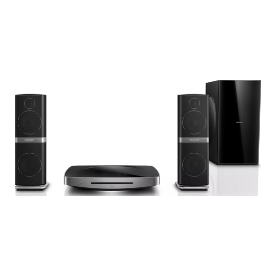
BD Home Theater System
Service
Service Manual
Copyright 2013Philips Consumer Electronics B.V. Eindhoven, The Netherlands
©
All rights reserved. No part of this publication may be reproduced, stored in a retrieval system or
transmitted, in any form or by any means, electronic, mechanical, photocopying, or otherwise
without the prior permission of Philips.
Published by
SL_HF1305
Service Audio Printed in The Netherlands Subject to modification
Version 1.1
TABLE OF CONTENTS
Location of PCB Boards ............................................ 1-2
Versions Variation ...................................................... 1-2
Specifications ............................................................ 1-3
Measurement Setup .................................................. 1-6
Service Aids .............................................................. 1-7
ESD & Safety Instruction .......................................... 1-8
Lead-free Soldering Information ................................ 1-9
Setting Procedure & Repair Instructions ...................... 2
Disassembly Instructions & Service Positions .............. 3
Block & Wiring Diagram ................................................ 4
BD Board........................................................................ 6
Touch Board .................................................................. 7
Power Board(Subwoofer) ............................................ 8
Mechanical Exploded View............................................ 9
Revision List ................................................................ 10
1 - 1
Chapter
HTB7250D_HTB7255D/
GB
3141 785 39441
12
under license.
Advertisement
Table of Contents

Related Manuals for Philips HTB7250D


Summary of Contents for Philips HTB7250D
-
Page 1: Table Of Contents
All rights reserved. No part of this publication may be reproduced, stored in a retrieval system or transmitted, in any form or by any means, electronic, mechanical, photocopying, or otherwise without the prior permission of Philips. 3141 785 39441 Published by... -
Page 2: Location Of Pcb Boards
MAIN PCB VFD PCB MP3 PCB SUB _POWR CPB USB PCB TOUCH PCB SENSOR PCB Main Unit Subwoofer VERSION VARIATION: Type/Versions HTB7250D HTB7255D Features Output Power - 500W Voltage (220~240V) Bluetooth Subwoofer SERVICE SCENARIO MATRIX: HTD7250D Type/Versions HTD7255D Board in used... -
Page 3: Specifications
1 - 3 SPECIFICATIONS Extension Con- Audio Bit rate Region codes tainer codec The type plate on the back or bottom of the .mp3 Upto 320 kbps home theater shows which regions it supports. .wma Upto 192 kbps WMA Pro Upto 768 kbps Country .aac AAC AAC, HE-... - Page 4 1 - 4 Audio codec Video codec Bit rate Audio Video codec Bit rate codec PCM, Dolby Digital, MPEG 1, 40 Mbps DTS core, MPEG, MPEG 2 PCM, DivX 3.11, DivX 4.x, 10 Mbps MP3, WMA, AAC, Dolby DivX 5.x, DivX 6.x HE-AAC, DD+ Digital, DTS core,...
- Page 5 1 - 5 Subwoofer • Total output power: 500W RMS (+/- 0.5 • Power supply: dB, 30% THD) / 400W RMS (+/- 0.5 dB, • Europe/China: 220-240 V~, 50 Hz 10% THD) • • Frequency response: 20 Hz-20 kHz / ±3 V/220-240 V~, 50/60 Hz •...
-
Page 6: Measurement Setup
1 - 6 MEASUREMENT SETUP Tuner FM Bandpass LF Voltmeter 250Hz-15kHz e.g. PM2534 e.g. 7122 707 48001 RF Generator e.g. PM5326 S/N and distortion meter e.g. Sound Technology ST1700B Use a bandpass filter to eliminate hum (50Hz, 100Hz) and disturbance from the pilottone (19kHz, 38kHz). Use Audio Signal Disc SBC429 4822 397 30184 (replaces test disc 3) -
Page 7: Service Aids
1 - 7 SERVICE AIDS Service Tools: Universal Torx driver holder .........4822 395 91019 Torx bit T10 150mm ...........4822 395 50456 Torx driver set T6-T20 .........4822 395 50145 Torx driver T10 extended ........4822 395 50423 Compact Disc: SBC426/426A Test disc 5 + 5A ......4822 397 30096 SBC442 Audio Burn-in test disc 1kHz ....4822 397 30155 SBC429 Audio Signals disc .........4822 397 30184 Dolby Pro-logic Test Disc ........4822 395 10216... - Page 8 1 - 8 WAARSCHUWING WARNING Alle IC’s en vele andere halfgeleiders zijn All ICs and many other semi-conductors are gevoelig voor electrostatische ontladingen susceptible to electrostatic discharges (ESD). (ESD). Careless handling during repair can reduce life Onzorgvuldig behandelen tijdens reparatie kan drastically.
- Page 9 • You will find this and more technical information Use only lead-free solder alloy Philips SAC305 with within the “magazine”, chapter “workshop news”. order code 0622 149 00106. If lead-free solder-paste is required, please contact the manufacturer of your For additional questions please contact your local solder-equipment.
- Page 10 Select <preference>. restarts.If it does not, disconnect the powercord for a few seconds d) Select <Change Password> <Confirm>, then press <OK> button c) At the philips support website, find your product and click on User and then reconnect it. on R/C.
- Page 11 2 - 2 2 - 2 REPAIR INSTRUCTIONS(main unit) HTB7225/9225 REPAIR CHART All Function Power Supply All Function Key board VFD board AUX IN MP3 In Tuner No Sound Subwoofer No Sound BT In Optical In No Working No Working No Sound No Function No Function...
- Page 12 2 - 3 2 - 3 REPAIR INSTRUCTIONS(BD Board) BD Board REPAIR CHART BD Function Loading All Video HDMI_RX no output No Working No DISC No OUTPUT BD function Loading All Video No OUTPUT No working No Disc loose Check CN4 cable is loose Re-insert and fix Check Y300 crystal Check JK805 is...
- Page 13 3 - 1 3 - 1 DISASSEMBLY INSTRUCTIONS-MAIN UNIT Dismantling of the VFD Board 1) Loosen 1 screws “D” on the top of VFD Board as shown in fi gure 4. Note:In some service positions the components or copper patterns of one board may risk touching its neighbouring pc boards or metallic parts.
- Page 14 3 - 2 3 - 2 Dismantling of the BD Board 1) Loosen 4 screws “H” on the top of BD Board as shown in fi gure 8. 2) Loosen 1screw “I” at the back panel as shown in fi gure 9. Figure 11 SERVICE POSITIONS (MAIN UNIT) Service Position A - MAIN&BD Board...
- Page 15 3 - 3 3 - 3 Dismantling of the Subwoofer AMP Board DISASSEMBLY INSTRUCTIONS-SUBWOOFER 1) Loosen 4 screws “S” on the top of subwoofer AMP board as shown in fi gure 19. Dismantling of the Subwoofer Rear Panel 1) Loosen 9 screws “Q” at the subwoofer rear panel as shown in fi gure 17. Figure 19 SERVICE POSITIONS (SUBWOOFER) Figure 17...
- Page 16 3 - 1 3 - 1 DISASSEMBLY INSTRUCTIONS-MAIN UNIT Dismantling of the VFD Board 1) Loosen 1 screws “D” on the top of VFD Board as shown in fi gure 4. Note:In some service positions the components or copper patterns of one board may risk touching its neighbouring pc boards or metallic parts.
- Page 17 3 - 2 3 - 2 Dismantling of the BD Board 1) Loosen 4 screws “H” on the top of BD Board as shown in fi gure 8. 2) Loosen 1screw “I” at the back panel as shown in fi gure 9. Figure 11 SERVICE POSITIONS (MAIN UNIT) Service Position A - MAIN&BD Board...
- Page 18 3 - 3 3 - 3 Dismantling of the Subwoofer AMP Board DISASSEMBLY INSTRUCTIONS-SUBWOOFER 1) Loosen 4 screws “S” on the top of subwoofer AMP board as shown in fi gure 19. Dismantling of the Subwoofer Rear Panel 1) Loosen 9 screws “Q” at the subwoofer rear panel as shown in fi gure 17. Figure 19 SERVICE POSITIONS (SUBWOOFER) Figure 17...
-
Page 19: Block & Wiring Diagram
4 - 1 4 - 1 BLOCK DIAGRAM HDMI IN + MPEG BOARD 7 KEY Display Unit Part Motor driver VFD Display +12V +12V (1.3A) LM1117-ADJ LED x 1 only STB for HTB72XX CEM8311/AO4813 8 - Char Only THB72XX TO OPU DDR3 (7.0A MOSFET SW IC) LED x 7 for HTB92XX... - Page 20 4 - 2 4 - 2 WIRING DIAGRAM AC SOCKET CN901...
-
Page 21: Main+Vfd+Sub+Usb+Mp3+Sensor+Bt Board
5 - 1 5 - 1 IC304 INTERNAL IC DIAGRAM - CS5346 CQZ 3.3 V to 5 V 3.3 V Left PGA Output ® ™ I²C /SPI Internal Voltage Control Data Right PGA Output Register Configuration Reference Interrupt Stereo Input 1 Stereo Input 2 Overflow Stereo Input 3... - Page 22 5 - 2 5 - 2 IC4103 INTERNAL IC DIAGRAM - TAS5538 DGG IC305 INTERNAL IC DIAGRAM - CS8422-CNZR QFN...
- Page 23 5 - 3 5 - 3 CIRCUIT DIAGRAM DP601 VFD_32P DP600 CN203 R2011 IR sensor VFD_45P HTB7251D Q2001 CN206 RB705 FB2017 600 R702 33 CN202 R2012 C706 FB201 CN4/20 C2014 FB2018 600 C703 ZD701 C707 RCI024004-0005 R278 33 24C16B R2013 Q3008 C221 C222...
- Page 24 5 - 4 5 - 4 PCB LAYOUT - TOP VIEW LFM110440-0001 HTB9225/7250 MAIN PCB 2012-12-20 O4.0 O4.0 O2.0 O2.0 O3.2 O3.2 O3.2 O3.2 O3.5 O3.5 Q3007 Q3006 RB805 RB5700 C343 C342 6.0X4.0 R3025 R304 R303 R309 R308 C5744 R5731 L-AUX-R C339 R3026...
- Page 25 5 - 5 5 - 5 PCB LAYOUT - BOTTOM VIEW D306 C853 C854 C5730 C696 D307 Q501 C5729 R504 C5745 C330 D502 R5717 C5727 C5318 D501 Q502 R505 C351 C705 C5314 R5312 C5725 C5327 R5722 R5315 C5325 C327 C5330 R5723 R5314 C5328...
-
Page 26: Bd Board
6 - 1 6 - 1 BLOCK DIAGRAM DDR3 128MB x 16 x 1 pcs BD OPU Sanyo TRV-415H09 DDR3 64MB x 16 x 2 pcs SERVO TPIC2050 Motor driver NAND Flash 2G bit (256MB) Ethernet USB2.0 Bus RJ-45 BD BOARD back USB2.0 USB 2.0 HDMI TMDS... - Page 27 6 - 2 6 - 2 Voltages for connector pin 2. J800--->>from BD board connect to BD loader(SERVO use) 4. CN203--->>from BD board connect to WIFI connect PCB 1. HA501--->>from BD board connect to main board PIN NO PIN Assign Remarks PIN NO PIN Assign...
- Page 28 6 - 3 6 - 3 Waveforms for measure point...
- Page 29 6 - 4 6 - 4 Waveforms for measure point...
-
Page 30: Touch Board
7 - 1 7 - 1 TOUCH BOARD TABLE OF CONTENTS Circuit Diagram .................. 7-2 PCB Layout Top & Bottom View ............7-3... - Page 31 7 - 2 7 - 2 CIRCUIT DIAGRAM FM140 +5.5V_LED CN1 CN8/110 PLAY POWE R VOL_DOWN VOL_UP STOP OPEN SOURCE BK3V3 Standb y SEN1N L_POWE R SEN0 N SEN0N IC1 IC_EKT4701_P32 DRV0 DRV0 SEN1 P DRV1 DRV1 DRV2 DRV2 R16 2K DRV3 Pxy_VF DRV3...
- Page 32 7 - 3 7 - 3 PCB LAYOUT - TOP VIEW LFA109300-0501 PCB LAYOUT - BOTTOM VIEW 3VDD +5.5V HTS9221_self_ISP_V02_0928...
- Page 33 8 - 1 8 - 1 IC905 INTERNAL IC DIAGRAM - AZ7500BP POWER BOARD TABLE OF CONTENTS Internal IC Diagram ................8-1 Circuit Diagram .................. 8-2 PCB Layout Top View ................ 8-3 PCB Layout Bottom View ..............8-4 IC903 INTERNAL IC DIAGRAM - SSC620S...
- Page 34 8 - 2 8 - 2 CIRCUIT DIAGRAM CN902 SCREW-A P906 P908 C946 470P-500V SCREW-A C976 T903 L-75UH CN9P-25 SCREW-A P905 P907 C155P-250V D923 L908 CN904 FB902 SW1A C954 AMP_VCC FMX22SL R910 SW-110/220V FB901 R956 R957A R957 C995 C994 C947 R946 R947 R948...
- Page 35 8 - 3 8 - 3 PCB LAYOUT - TOP VIEW WARNING: FOR CONTINUED PROTECTION AGAINST RISK OF FIRE REPLACE WITH SAME TYPE FUSE. HTAT1 P908 C986 C991 CN902 J903 Q902 R930 Q903 J904 Q901 TVR902 R917 R920 R924 T903 C976 C918 BD901...
- Page 36 8 - 4 8 - 4 PCB LAYOUT - BOTTOM VIEW C909 MARK2 R927 ZD903 R928 D904 ZD904 C911 C913 IC903 R909 R903A R910 R910A C901 C917 R949 IC901 R940 C931 C945 R949B C948 C935 R945 R942 C942 R944 R941 R963 Q907 R990...
- Page 37 10 - 1 10- 1 Mechanical Exploded View(Main Unit) Note: A1=12+4+7+8+9+25+SW2...
- Page 38 10- 2 10- 2 Mechanical Exploded View(Subwoofer) SW11 SW10 SW12 SW13...
- Page 39 10- 1 REVISION LIST Version 1.0 *Initial release Version 1.1 *Add HTB7255D/12 version...