
Related Manuals for Toshiba 30HFX84


Summary of Contents for Toshiba 30HFX84
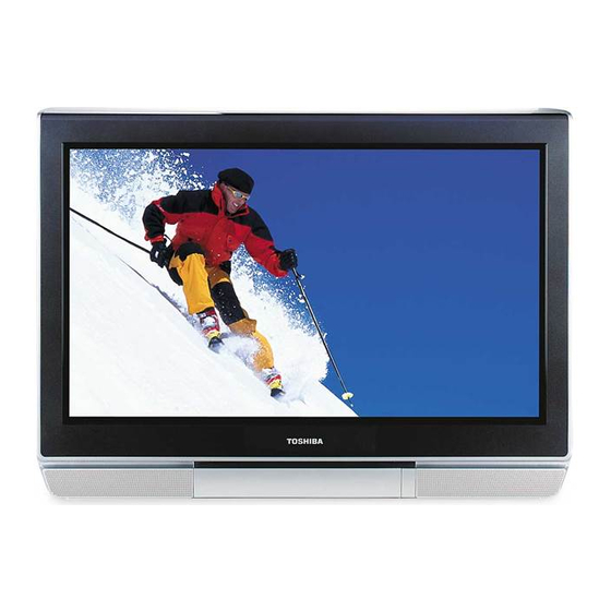
- Page 1 FILE NO. 050-200419 SERVICE MANUAL COLOR TELEVISION 30HFX84 DOCUMENT CREATED IN JAPAN, Aug., 2004...
-
Page 2: Servicing Notices On Checking
SERVICING NOTICES ON CHECKING 1. KEEP THE NOTICES 6. AVOID AN X-RAY As for the places which need special attentions, Safety is secured against an X-ray by consider- they are indicated with the labels or seals on the ing about the cathode-ray tube and the high cabinet, chassis and parts. -
Page 3: About Lead Free Solder (Pbf)
ABOUT LEAD FREE SOLDER (PbF) Distinction of PbF PCB: PCBs (manufactured) using lead free solder will have a PbF printing on the PCB. (Please refer to figures.) Caution: • Pb free solder has a higher melting point than standard solder; Typically the melting point is 50°F~70°F(30°C~40°C) higher. -
Page 4: Table Of Contents
TABLE OF CONTENTS SERVICING NOTICES ON CHECKING ..................A1-1 HOW TO ORDER PARTS ......................A1-1 IMPORTANT ..........................A1-1 ABOUT LEAD FREE SOLDER (PbF) ..................A1-2 TABLE OF CONTENTS ......................A2-1 GENERAL SPECIFICATIONS ....................A3-1~A3-5 DISASSEMBLY INSTRUCTIONS 1. REMOVAL OF ANODE CAP ....................B1-1 2. -
Page 5: General Specifications
GENERAL SPECIFICATIONS CRT Size / Visual Size 30 inch / 760mmV System CRT Type Flat (16:9) Deflection degree Magnetic Field BV/BH +0.45G/0.18G Color System NTSC Speaker 2 Speaker Position Front Bottom Size 1.8 x 3.9 Inch Impedance Sound Output 10W+10W 10%(Typical) NTSC3.58+4.43 /PAL60Hz Tuning... - Page 6 GENERAL SPECIFICATIONS On Screen Menu Display Menu Type Icon Picture Mode(Picture preference) Brightness Contrast Color Tint Sharpness Color Temperature Display Format Cable Clear Reset Audio Bass Treble Balance Stable Sound Speakers On/Off Dolby Virtual WOW SRS 3D WOW Focus WOW Tru Bass HDMI1 HDMI2 Reset...
- Page 7 Timer Back-up (at Power Off Mode) more than G-10 Remote Unit RC-JW Control Glow in Dark Remocon Back Light Remocon Format Toshiba Custom Code TV:40-BFh Power Source Voltage(D.C) UM size x pcs UM-3 x 2 pcs Total Keys Keys Keys...
- Page 8 GENERAL SPECIFICATIONS G-11 Features Auto Degauss Auto Shut Off CABLE Memory(Last CH) Memory(Last Volume) V-Chip Type USA, ORION Type SRS WOW(SRS 3D/Focus/Tru Bass) Timer(On Timer /Sleep Timer) Aspect Cinema Mode Image Tilt Direct Input Selection Auto Search CH Allocation CH Lock CH Program CH Label Just Clock Function...
- Page 9 GENERAL SPECIFICATIONS G-13 Interface Switch Front Power Channel Up/Menu Up Channel Down/Menu Down Volume Up/Menu > Volume Down/Menu < Rear AC/DC TV/CABLE Selector Degauss Main Power SW Indicator Power Yes(RED) Stand-by On Timer Terminals Front Video Input = VIDEO3 Audio Input = VIDEO3 RCA x 2 S Input = VIDEO3 Other Terminal...
-
Page 10: Disassembly Instructions
DISASSEMBLY INSTRUCTIONS 3. After one side is removed, pull in the opposite direction to 1. REMOVAL OF ANODE CAP remove the other. Read the following NOTED items before starting work. NOTE After turning the power off there might still be a potential Take care not to damage the Rubber Cap. -
Page 11: Removal And Installation Of Flat Package Ic
DISASSEMBLY INSTRUCTIONS When IC starts moving back and forth easily after REMOVAL AND INSTALLATION OF desoldering completely, pickup the corner of the IC using a FLAT PACKAGE IC tweezers and remove the IC by moving with the IC desoldering machine. (Refer to Fig. 2-3.) REMOVAL NOTE Put the Masking Tape (cotton tape) around the Flat... - Page 12 DISASSEMBLY INSTRUCTIONS INSTALLATION When bridge-soldering between terminals and/or the soldering amount are not enough, resolder using a Thin-tip Take care of the polarity of new IC and then install the new Soldering Iron. (Refer to Fig. 2-8.) IC fitting on the printed circuit pattern. Then solder each lead on the diagonal positions of IC temporarily.
-
Page 13: Service Mode List
SERVICE MODE LIST This unit provided with the following SERVICE MODES so you can repair, examine and adjust easily. To enter the Service Mode, press both set key and remote control key for more than 2 seconds. Set Key Remocon Key Operations Releasing of V-CHIP PASSWORD. -
Page 14: When Replacing Eeprom (Memory) Ic
WHEN REPLACING EEPROM (MEMORY) IC If a service repair is undertaken where it has been required to change the MEMORY IC, the following steps should be taken to ensure correct data settings while making reference to TABLE 1. ADDRESS DATA INIT CRT ON 0010 OEC7111A_073... -
Page 15: Electrical Adjustments
ELECTRICAL ADJUSTMENTS 1. ADJUSTMENT PROCEDURE FUNCTION FUNCTION FUNCTION OSD H CORNER R-Y PHASE Read and perform these adjustments when repairing the CUT OFF C.PARA G-Y GAIN circuits or replacing electrical parts or PCB assemblies. H.POSI C.SAW G-Y PHASE V.POSI V.SYMM BRI.CENT CAUTION H. - Page 16 ELECTRICAL ADJUSTMENTS 2-3: DOUBLE FOCUS 2-5: HORIZONTAL POSITION/ HORIZONTAL SIZE Receive the cross hatch signal from the Pattern Receive the monoscope pattern. Generator. Press the MENU button. And, then press the LEFT/ Turn the F1 VR and F2 VR fully clockwise once. (Refer RIGHT button on the remote control until the PICTURE to Fig.
- Page 17 ELECTRICAL ADJUSTMENTS 2-7: VERTICAL LINEARITY 2-10: E/W PARA Receive the crosshatch signal from the Pattern Generator. NOTE: Adjust after performing adjustments in section 2-6. Set the screen mode to FULL. After the adjustment of Vertical Linearity, reconfirm Using the remote control, set the brightness and contrast the Vertical Position and Vertical Size adjustments.
- Page 18 ELECTRICAL ADJUSTMENTS 2-13: TINT/COLOR CENT 2-14: TILT Connect the digital voltmeter between W843 and W844. Receive the color bar pattern. Receive the crosshatch signal from the Pattern Generator. Connect the oscilloscope to TP806. Press the PIC SIZE button on the remote control to select Activate the adjustment mode display of Fig.
- Page 19 ELECTRICAL ADJUSTMENTS 3. PURITY AND CONVERGENCE 3-3: STATIC CONVERGENCE ADJUSTMENTS NOTE Adjust after performing adjustments in section 3-2. NOTE Receive the crosshatch pattern from the color bar Turn the unit on and let it warm up for at least 30 generator.
- Page 20 ELECTRICAL ADJUSTMENTS 4. ELECTRICAL ADJUSTMENT PARTS LOCATION GUIDE (WIRING CONNECTION) CP804 R841 VM COIL PCB J801 CP853 S853 S854 CP852 CP808B CRT PCB CP802B CP851B MAIN PCB AV PCB PCB J705 CP808A FB401 CP103 J709 J708 J707 J706 CP510 CP404 CP102 CP712 CP703B...
-
Page 21: Sound Amp/Front Jack
TV BLOCK DIAGRAM CD507 DEGAUSS COIL TRANSFORMER D506, D507 F501 T501 D510, D511 AT+5V MICON1/ CD501 STEREO AT+3.3V AT+5V SENC COUNT/ CONNECTOR REGURATOR IC505 KI278R09PI D520, D521 D522, D523 TRANSFORMER D525, D526 T502 D527, D528 REGURATOR IC506 SOUND AMP/ KIA431A-AT SOUND+B FRONT JACK FEED BACK... - Page 22 SOUND AMP/FRONT JACK BLOCK DIAGRAM SOUND AMP IC IC1001 AN7522N VOUTP1 OAOUT1 SPEAKER SP1001 AUDIO_L INV1 OUTM1 OAOUT2 OUTM2 MICOM1/ SPEAKER STEREO AUDIO_R INV2 SP1002 VOUTP2 AUDIO_MUTE MUTE VDDA VDD1 VDD1 VDD2 SOUND+B VDD2 FRONT JACK FRONT_A_IN_R J2204 FRONT JACK FRONT_A_IN_L J2203 SYNC COUNT/...
- Page 23 MICON1/STEREO BLOCK DIAGRAM SYSTEM RESET MICON IC101 OEC7111A IC102 PST3229NR SCL1 RESET SCL1 SDA1 SDA1 Xout D101 SDA2 31 SDA2 X103 SYNC COUNT/ EEP ROM IC 64K 16MHz SCL2 28 SCL2 CONNECTOR IC199 BR24L64F-WE2 VCC(5V) AT+5V EEPROM_SCL VCC(3.3V) 16 AT+3.3V EEPROM_SDA EEP_DATA OSD_R 32...
-
Page 24: Av/Sync Count/Connector
AV/SYNC COUNT/CONNECTOR BLOCK DIAGRM YUV_SW YUV IC IC706 CS_IN1 IC702 NJM2584AM(TE1) NJM2584AM(TE1) J706 CP3604A IN3A IN1A IN1B IN1A IN2A IN3B IN2A +12V IN2B IN3A DAC_A_L IN2B INTRFACE DAC_A_R P.CON+5V OUT IN1B IC3401 KIA278O05PI IN3B CS_IN2 AUDIO-L J707 AUDIO-R AT+5V UNREG+8V P.CON+9V OUT UNREG+12V IC3400 KIA78R09PI... - Page 25 INTERFACE1 BLOCK DIAGRAM EEP_ROM IC3606 S-24C02BFJ-TB ANBPB INTERFACE2 ANGY ANRPR HDMI INTERFACE IC3605 SiI9993CTG100 CP3602 Q3603 AnBPb 15 BUFFER DSDA AnGY 12 +12V Q3604 AnRPr SYNC COUNT/ DAC_A_L BUFFER DSCL CONNECTOR HDMI1 DAC_A_R CONNECTOR CP3601 Q3617 Q3618 VSYNC 19 DET AUDIO-L 18 POWER AUDIO-R...
-
Page 26: Interface1
INTERFACE2 BLOCK DIAGRAM EEP_ROM IC3610 S-24C02BFJ-TB HDMI INTERFACE IC3609 SiI9993CTG100 Q3612 AnBPb 15 An BPd BUFFER DSDA INTERFACE1 AnGY 12 An GY Q3614 An RPr AnRPr DSCL BUFFER HDMI2 CONNECTOR CP3603 Q3619 Q3620 VSYNC 19 DET 18 POWER 17 GND L3605 ACM2012D MCLK... -
Page 27: Interface2
MICON2 BLOCK DIAGRAM HDMI MICON IC IC3611 SST89C58-33-TQJ H2_INT 36 H2_INT INTERFACE2 RXT2_RST# 8 RX2_RST RXT_RST# 36 RX1_RST X3601 11.0592MHz H_INT RX1_INT 38 VCC IC3612 SN74AHC1G08DCKR EA-/VPP Q3606 V-SYNC CSDA BUFFER 3 CSDA V_SYNC EEP ROM IC IC3608 BR24L32F-WE2 Q3609 Q3608 MUTE_CTL MUTE SW... -
Page 28: Printed Circuit Boards Main
PRINTED CIRCUIT BOARDS MAIN (INSERTED PARTS) SOLDER SIDE CP1003 CD101 CP510 CD605 W844 D617 R404 CD601 R417 R638 C569_1 W843 W839 IC602 R623 W045 W047 R487 W826 D424 W821 D618 W024 W025 IC401 D616 W055 W023 W836 D610 W808 W001 W841 W022 Q413... - Page 29 PRINTED CIRCUIT BOARDS MAIN (INSERTED PARTS) SOLDER SIDE R465 R446 R409 R461 R533 R537 R534 Q510 R542 Q501 R502 Q2001 Q615 Q617 Q616 Q606 Q605 Q607 Q608 R475 Q414 Q410 R686 Q611 R684 R642 R633 Q612 CMD003B Q407 Q408 Q406 Q405 Q601 R643 R497...
-
Page 30: Av/Connector
PRINTED CIRCUIT BOARDS AV/CONNECTOR (INSERTED PARTS) AV/CONNECTOR (CHIP MOUNTED PARTS) SOLDER SIDE SOLDER SIDE CED010B CONNECTOR CD706 W803 W808 R006 R004 R005 R717 Q702 R715 Q716 R788 R789 CP705 Q703 Q717 W806 CP703A CP702A RISK OF FIRE - REPLACE AS MARKED. Q701 Q3403 R704... -
Page 31: Hd-Mi
PRINTED CIRCUIT BOARDS HD-MI (TOP SIDE) HD-MI (BOTTOMSIDE) HS3601 IC3606 Q3603 Q3607 R3693 R3705 CP3604 B3601 L3601 L3603 Q3617 Q3618 L3602 Q3605 L3604 Q3606 IC3602 R3641 MICON C3638 NTSC CED013A CED013A X3601 D3613 C3643 C3642 R3619 REFLOW B3603 R3647 HS3602 R3653 Q3612 Q3616... -
Page 32: Front Jack
PRINTED CIRCUIT BOARDS FRONT JACK (TOP SIDE) FRONT JACK (BOTTOM SIDE) CD2201 CED008A CED008A CD1003 W808 CD1004 CD1001 JACK Q1002 CD2251 REFLOW NTSC C1014 C1016 IC1001 f-10... -
Page 33: Crt
PRINTED CIRCUIT BOARDS CRT/VM COIL SOLDER SIDE R802 TP804 D807 D808 R835 R801 R824 R825 R817 C804 C805 R818 R819 W009 R820 HS808 R834 W004 W815 TP805 D802 Q805 Q801 W005 D801 HS804 D816 W811 D811 R808 R806 Q810_1 Q811_1 Q807 Q802 D824... -
Page 34: Sound Amp/Front Av
WAVEFORMS CHROMA/PROGRESSIVE/ PIN CUSHION 10µs 10µs 1.0V 0.5V 1.0V DEFLECTION 20µs 10µs 10µs 2.0V 1.0V 1.0V 10µs 10µs 0.5V 1.0V 1.0V 10µs 1.0V 5.0V 0.5V SOUND AMP/ FRONT AV 10µs 20µs 200m 0.5V 1.0V NOTE: The following waveforms were measured at the point of the corresponding balloon number in the schematic diagram. -
Page 35: Micon1
WAVEFORMS MICON1 20ms 200m 1.0V 1.0V STEREO 20ms 0.5ms 1.0V 200mV 1.0V 10ms 20ms 1.0V 200mV 1.0V SYNC COUNT/ CONNECTOR 20µs 20ms 1.0V 1.0V 1.0V 20µs 20ms 1.0V 1.0V 1.0V NOTE: The following waveforms were measured at the point of the corresponding balloon number in the schematic diagram. -
Page 36: Crt/Cvm
WAVEFORMS 10µs 20µs 20µs 200mV 1.0V 1.0V 10µs 20µs 20µs 200mV 1.0V 20µs 20µs 500µs 200mV 1.0V CRT/CVM 20µs 500µs 20µs 1.0V 200mV INTERFACE MICON2 10µs 20µs 500µs 200mV 1.0V 1.0V NOTE: The following waveforms were measured at the point of the corresponding balloon number in the schematic diagram. - Page 37 WAVEFORMS 500µs 1.0V NOTE: The following waveforms were measured at the point of the corresponding balloon number in the schematic diagram.
-
Page 38: Mechanical Exploded Views
MECHANICAL EXPLODED VIEW PCB110 (CRT PCB ASS'Y) PCBD80 (VM COIL PCB ASS'Y) 101I 101J 101H 101D 101L 101K 101B PCB260 101K (FRONT JACK PCB ASS'Y) 101K 101A 101H 101G 101K 101E 101F 101C... - Page 39 MECHANICAL EXPLODED VIEW 205 206 102B 102C 102A 102C PCB070 (MAIN PCB ASS'Y) PCBDJ0 (HD-MI PCB ASS'Y) PCBDI0 (CONNECTOR PCB ASS'Y) PCBD20 (AV PCB ASS'Y)
- Page 40 MECHANICAL EXPLODED VIEW (PACKING DIAGRAM) 131, 132, 133, 134, TM101...
-
Page 41: Mechanical Replacement Parts List
MECHANICAL REPLACEMENT PARTS LIST Location No. TSB P/N Reference No. Description AE005197 7A7010039A FRONT CABI ASS'Y 101A AE005198 701WPJ1301 CABINET,FRONT 101B AE004821 711WPA0210 PLATE,FRONT 101C AE005199 712WPJ0890 DOOR 101D AE004823 713WPA0334 GUIDE,REMOCON 101E AE004824 7230007791 SHEET,BUTTON 101F AE004825 7230007792 AV LABEL 101G AD302008 7235490036... -
Page 42: Electrical Replacement Parts List
ELECTRICAL REPLACEMENT PARTS LIST Location No. TSB P/N Reference No. Description RESISTORS ! R401 AE002516 R4X5T6222F R,METAL 2.2K OHM 1/6W ! R403 BZ210105 R4X5T6183F R,METAL 18K OHM 1/6W ! R405 BZ210231 R4X5T6153F R,METAL 15K OHM 1/6W ! R406 AD300039 R3X18A680J R,METAL OXIDE OHM 2W ! R408... - Page 43 ELECTRICAL REPLACEMENT PARTS LIST Location No. TSB P/N Reference No. Description CAPACITORS ! C548 BZ110055 E5EZF4102M 1000 UF 35V C549 BZ110183 C03L0R7W2K 820 PF 2KV R C567 BZ110209 E0ELF3222M 2200 UF 25V C808 AE003828 C13DB0713K 0.001 UF 2KV B C809 AD301347 E0ELFD330M UF 250V...
- Page 44 ELECTRICAL REPLACEMENT PARTS LIST Location No. TSB P/N Reference No. Description DIODES D544 BZ410006 D1VT001330 DIODE,SILICON 1SS133T-77 D546 BZ410006 D1VT001330 DIODE,SILICON 1SS133T-77 D547 BZ410084 D97U01101B DIODE,ZENER MTZJ11B T-77 D548 BZ410006 D1VT001330 DIODE,SILICON 1SS133T-77 D549 BZ410037 D97U03301B DIODE,ZENER MTZJ33B T-77 D550 BZ410021 D97U05R61B DIODE,ZENER...
- Page 45 ELECTRICAL REPLACEMENT PARTS LIST Location No. TSB P/N Reference No. Description DIODES D3619 AE004795 DE7RB5R62B DIODE,ZENER UDZS5.6B TE-17 D3620 AE004937 D77R1A1R10 DIODE,VARISTA AVRL161A1R1NT D3621 AE004793 DD7R60L400 DIODE,SCHOTTKY RB160L-40-TE25 D3623 AE004793 DD7R60L400 DIODE,SCHOTTKY RB160L-40-TE25 IC101 AE004804 I56F57111A OEC7111A IC102 79097849 I9UF032290 PST3229NR IC199 AE005238...
- Page 46 ELECTRICAL REPLACEMENT PARTS LIST Location No. TSB P/N Reference No. Description TRANSISTORS Q613 AE002626 T8YJ2412K0 TRANSISTOR,SILICON 2SC2412KT146 R,S Q615 BZ510108 TAAA1504SY TRANSISTOR,SILICON KTA1504S_Y_RTK Q616 BZ510108 TAAA1504SY TRANSISTOR,SILICON KTA1504S_Y_RTK Q617 BZ510108 TAAA1504SY TRANSISTOR,SILICON KTA1504S_Y_RTK Q701 BZ510109 TCAA3875SY TRANSISTOR,SILICON KTC3875S_Y_RTK Q702 BZ510108 TAAA1504SY TRANSISTOR,SILICON KTA1504S_Y_RTK...
- Page 47 ELECTRICAL REPLACEMENT PARTS LIST Location No. TSB P/N Reference No. Description COILS &TRANSFORMERS L607 BZ310039 02167F220J COIL L651 BZ310118 02AHB9A972 CORE,FERRITE W5T29X7.5X19 L701 BZ310040 02167F470J COIL L702 BZ310040 02167F470J COIL L703 BZ310040 02167F470J COIL L705 BZ310041 02167F101J COIL 100 UH L706 BZ310040 02167F470J...
- Page 48 ELECTRICAL REPLACEMENT PARTS LIST Location No. TSB P/N Reference No. Description MISCELLANEOUS B852 BZ310121 024HT03553 CORE,BEADS W5RH3.5X5X1.0 B853 BZ310121 024HT03553 CORE,BEADS W5RH3.5X5X1.0 B3601 AE004602 024HC36001 CORE,BEADS HCB2012K-600T25 B3602 AE004602 024HC36001 CORE,BEADS HCB2012K-600T25 B3603 AE004602 024HC36001 CORE,BEADS HCB2012K-600T25 B3604 AE004602 024HC36001 CORE,BEADS HCB2012K-600T25 B3608...
- Page 49 ELECTRICAL REPLACEMENT PARTS LIST Location No. TSB P/N Reference No. Description MISCELLANEOUS EL1101 BZ614043 124116281A EYE LET XRY16X28BD EL1102 BZ614044 124120301A EYE LET XRY20X30BD ! F501 BZ614422 081PC6R305 FUSE 51MS063L ! F502 AE004346 0835A07005 MICRO FUSE 20N_7000FSW ! F3401 AE004954 0835C01003 MICRO FUSE 20N_1000FS...
- Page 50 TOSHIBA CORPORATION 1-1, SHIBAURA 1-CHOME, MINATO-KU, TOKYO 105-8001, JAPAN...