Advertisement
SERVICE MANUAL
2012
4 S ERVICE MANUAL
MA503<Rev.003>
KD-R430J, KD-R431E, KD-R431EN, KD-R431EU,
KD-R431EY, KD-R432E, KD-R432EN, KD-R432EU,
KD-R432EY, KD-R434UI, KD-R435U, KD-R435UN,
KD-R436U, KD-R436UN, KD-R436UP,
KD-R437EE, KD-R439UR, KD-R48EE, KD-R531E,
KD-R531EN, KD-R531EU, KD-R531EY, KD-R54J
KD-R430, KD-R434,
KD-R435, KD-R435,
KD-R436, KD-R436,
KD-R436, KD-R439,
COPYRIGHT © 2012 JVC KENWOOD Corporation
Lead free solder used in the board (material : Sn-Ag-Cu, melting point : 219 Centigrade)
Lead free solder used in the board (material : Sn-Cu, melting point : 230 Centigrade)
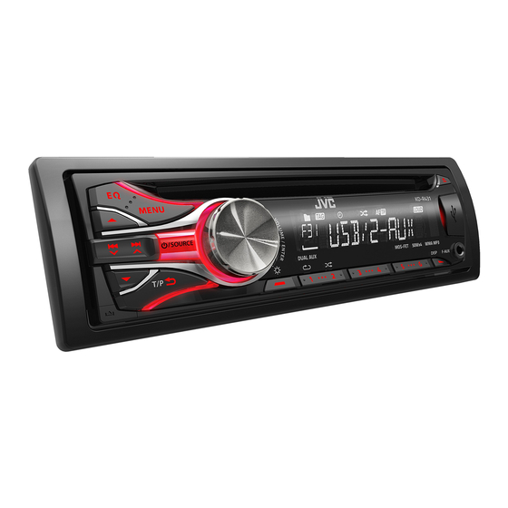
CD RECEIVER
For KD-R430,KD-R431,
For
KD-R432,KD-R435,KD-R436,
KD-R437,KD-R48,KD-R531,
KD-R54
KD-R54
For
KD-R531,KD-R432,KD-R431
For KD-R430,KD-R54
COPYRIGHT © 2012 JVC KENWOOD Corporation
DETACH PANEL
Model
Parts number
KD-R430J
CP-R430JD
KD-R431E
CP-R431ED
KD-R431EN
CP-R431ED
KD-R431EU
CP-R431ED
KD-R431EY
CP-R431ED
KD-R432E
CP-R432ED
KD-R432EN
CP-R432ED
KD-R432EU
CP-R432ED
KD-R432EY
CP-R432ED
KD-R434UI
CP-R434UID
CP-R435UD
KD-R435U
KD-R435UN
CP-R435UD
KD-R436U
CP-R436UD
KD-R436UN
CP-R436UD
KD-R436UP
CP-R436UD
KD-R437EE
CP-R437EED
KD-R438J
CP-R438JD
KD-R438UF
CP-R438UFD
KD-R48EE
CP-R48EED
KD-R531E
CP-R531ED
KD-R531EN
CP-R531ED
KD-R531EU
CP-R531ED
KD-R531EY
CP-R531ED
KD-R54J
CP-R54JD
No.MA503<Rev.003>
2012/4
Advertisement
Table of Contents

Related Manuals for JVC KD-R430J


Summary of Contents for JVC KD-R430J
- Page 1 CP-R531ED KD-R54J CP-R54JD COPYRIGHT © 2012 JVC KENWOOD Corporation Lead free solder used in the board (material : Sn-Ag-Cu, melting point : 219 Centigrade) Lead free solder used in the board (material : Sn-Cu, melting point : 230 Centigrade) No.MA503<Rev.003>...
-
Page 2: Audio Amplifier Section
SPECIFICATION For US AUDIO AMPLIFIER SECTION 20 W RMS x 4 Channels at 4 Ω and ≤ 1% THD+N Power Output 4 Ω (4 Ω to 8 Ω allowance) Load Impedance Frequency Response 40 Hz to 20 000 Hz Signal-to-Noise Ratio 80 dBA (reference: 1 W into 4Ω) Line-Out or Subwoofer-Out Level/Impedance 2.5 V/20 kΩ... -
Page 3: Tuner Section
SPECIFICATION For ASIA AUDIO AMPLIFIER SECTION Maximum Power Output 50 W per channel Continuous Power Output (RMS) 20 W per channel into 4Ω, 40 Hz to 20 000 Hz at less than 1% total harmonic distortion. Load Impedance 4 Ω (4 Ω to 8 Ω allowance) Frequency Response 40 Hz to 20 000 Hz Signal-to-Noise Ratio... - Page 4 SPECIFICATION For EUROPE AUDIO AMPLIFIER SECTION Maximum Power Output 50 W per channel Continuous Power Output (RMS) 20 W per channel into 4Ω, 40 Hz to 20 000 Hz at less than 1% total harmonic distortion. Load Impedance 4 Ω (4 Ω to 8 Ω allowance) Frequency Response 40 Hz to 20 000 Hz Signal-to-Noise Ratio...
- Page 5 SECTION 1 PRECAUTION Safety Precautions (1) This design of this product contains special hardware and voltmeter. many circuits and components specially for safety purpos- Move the resistor connection to each exposed metal es. For continued protection, no changes should be made part, particularly any exposed metal part having a return to the original design unless authorized in writing by the path to the chassis, and measure the AC voltage across...
- Page 6 Preventing static electricity Electrostatic discharge (ESD), which occurs when static electricity stored in the body, fabric, etc. is discharged, can destroy the laser diode in the traverse unit (optical pickup). Take care to prevent this when performing repairs. 1.5.1 Grounding to prevent damage by static electricity Static electricity in the work area can destroy the optical pickup (laser diode) in devices such as laser products.
- Page 7 Important for laser products 1.CLASS 1 LASER PRODUCT 5.CAUTION : If safety switches malfunction, the laser is able to function. 2.CAUTION : (For U.S.A.) Visible and/or invisible class II laser radiation 6.CAUTION : Use of controls, adjustments or performance of when open.
- Page 8 SECTION 2 SPECIFIC SERVICE INSTRUCTIONS This service manual does not describe SPECIFIC SERVICE INSTRUCTIONS. SECTION 3 DISASSEMBLY Main body (Used model: KD-R431) (2) Remove the 2 screws B attaching both sides of the Top chassis. (See Fig.4) 3.1.1 Removing the Bottom chassis (See Fig.1) (1) Disengage the 7 hooks a engaging the Bottom chassis.
- Page 9 3.1.4 Removing the CD mechanism (See Fig.6) CD mechanism assembly section (1) Remove the 3 screws D attaching the CD mechanism. 3.2.1 Removing the Mecha control board (1) Solder the short land on the pickup. (See Fig. 1) SOLDER Fig.1 (2) Remove the 8 wires from the Mecha control board.
- Page 10 3.2.2 Removing the Traverse mechanism (See Fig.4, 5) (2) Remove the shaft from the TM base. (See Fig.7) (1) Remove the 5 springs from the traverse mechanism. (See (3) Disengage the hook a on the pickup from the TM base. Fig.4) (See Fig.7) shaft...
- Page 11 (2) Remove the HC CL. base from the holes on the TM base. 3.2.5 Removing the Loading motor (See Fig.9) (1) Remove the roller arm assembly from the bottom frame as- sembly. (See Fig.11) Fig.9 (3) Remove the 2 screws D attaching the spindle motor. (See Fig.10) Fig.11 (2) Remove the 2 screws E attaching the loading motor as-...
-
Page 12: Section 4 Adjustment
SECTION 4 ADJUSTMENT Service Test mode Default status immediately after the mode activation Operating Key : [MENU] → [DOWN] (7sec) 4.1.1 Mode content Syscon shall display the following information after entering this mode. The operation shown below shall be workable. Display content Detail The display is released when another operation is executed. - Page 13 4.1.3 CD error information display mode Operation Display content Detail CD mecha error Mecha error history 1,2,3 (latest) log display # = History No. (1,2,3) XX : kind of errors, " -- " when there is none. 00: No Error 04: TOC read Error 05: Unknown CD 06: Heat Error...
- Page 14 DC error information mode * The receiver is connected with the DC power supply (with the power supply turned off). Operating Key : [MENU] → [UP] → [DC power supply turned ON] 4.2.1 Mode content Syscon shall display the following information after entering this mode. The operation shown below shall be workable. Display content Detail When DC error is detected (in case that one of capacitor leakage, wrong...
-
Page 15: Section 5 Troubleshooting
DC Offset error description 4.3.5 Manipulate after detect DC Offset • If detected error 10 consecutive times, and 10th error occurred 4.3.1 DC Offset detection circuit design in "Mis-connect detection period", judge as "Mis-connect". • Purpose: • If detected error 10 consecutive times, and 10th error occurred To prevent breakdown, burning and emitting smoke from cus- in "Capacitor leak detection period", judge as "Capacitor leak ". - Page 16 JVC KENWOOD Corporation Car Electronics Business Group 2967-3, Ishikawa-machi, Hachioji-shi, Tokyo, 192-8525, Japan (No.MA503<Rev.003>) Printed in Japan...