Table of Contents
Advertisement
Quick Links
Advertisement
Table of Contents

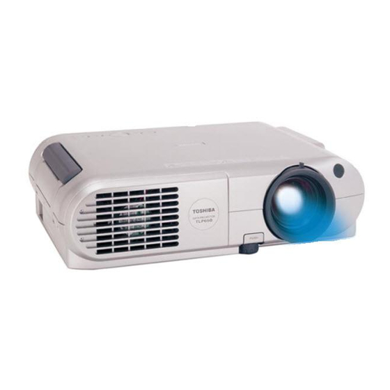
Related Manuals for Toshiba TLP-MT1


Summary of Contents for Toshiba TLP-MT1
- Page 1 TLP-MT1 — S U M M A R Y — TLP-MT1 is based on TLP450E and TLP450U. This service manual covers only different portions from service manual (File No. 333-9904) for TLP450E and TLP450U. PRINTED IN JAPAN, Dec., 1999 CS...
- Page 2 The following parts list covers only the different parts from the base models. For the other parts, please refer to the service manual (File No. 330-9904) of the base models. Location Part No. Description A400 23064069 Case A302 23550982 Rating Label A300 23550983 Front Tag...
- Page 3 FILE NO. 330-9904 SERVICE MANUAL 3LCD DATA PROJECTOR TLP450E, TLP451E TLP650E, TLP651E TLP450U, TLP451U TLP650U, TLP651U TLP451, TLP651 PRINTED IN JAPAN, Oct., 1999...
-
Page 4: Table Of Contents
CONTENTS SAFETY PRECAUTIONS .............. I IMPORTANT PRECAUTIONS ............ I IMPORTANT SAFETY INSTRUCTIONS ......II SECTION 1 PART REPLACEMENT AND ADJUSTMENT PROCEDURES 3-11. Input PC Board ............... 1-6 1 . LOCATION OF MAIN PARTS ......... 1 - 1 2 . LOCATION OF PC BOARDS ........... 1 - 1 3-12. -
Page 5: Location Of Main Parts
SECTION 1 PART REPLACEMENT AND ADJUSTMENT PROCEDURES 1. LOCATION OF MAIN PARTS TLP451/651 E200 Optical Engine PC300 Camera Unit Assembly B180 Lamp House P800 Power Unit Z101 Fan SC01 Arm Position Detection Switch P100 Thermal Lead Switch LCD Block Projection Lens Filter Fig. -
Page 6: Replacement Of Mechanical Parts
CAUTIONS BEFORE STARTING SERVICING Electronic parts are susceptible to static electricity and may easily damaged, so do not forget to take a proper grounding treatment as required. Many screws are used inside the unit. To prevent missing, dropping, etc. of the screws, always use a magnetized screwdriver in servicing. -
Page 7: Front Cover And Top Cover
3-3. Front Cover and Top Cover Screws (4) Main PC board (1) Connectors (2) 1. Remove two screws (1) and remove the front cover (2) by sliding the portion A pushed with a thin bar in the arrow B direction. 2. -
Page 8: Handle And Fan Assembly
3-6. Handle and Fan Assembly 3-7. Power Supply Unit 1. Pull out the handle (1) upward. 1. Remove two screws (1) and then remove the shield plate (2) and the socket (3). (Do not lose the shield 2. Remove two screws (2) and fan assembly (3). plate (2).) 3. -
Page 9: Filter Assembly
Temperature 3-8. Filter Assembly Screw (4) sensor switch (5) 1. Remove the filter cover (1) from the suction fan Screw (1) holder (2). 2. Remove the filters (3) and (4) from the filter cover (1). Lamp house (3) (When replacing and/or cleaning the filter, note the arrangement of the filters. - Page 10 3-11. Input PC Board 3-13. Mirror Box 1. Remove five screws (1). 1. Remove three screws (1) and then remove the mirror box (2). 2. Remove the input PC board (2) by turning the arrow direction. Screws (1) Screws (1) Input PC board (2) Mirror box (2) Fig.
- Page 11 3-14. LCD Block and LCD Panel 3. Mount a holder support for the service holder at the location of the panel holder removed. (Use screws 1. Remove three screws (1) and remove the LCD block (2). removed in step 2.) (Refer to Fig. 1-3-16 for the 2.
- Page 12 < Holder fixing > 2. Tighten the S adjusting screws with a wrench for servicing and fix the Z rotation plate. (Refer to Fig. 1- 1. Apply screw lock to the S adjusting screws. 3-17.) If the focus adjusted is upset when fixing, 2.
- Page 13 3-15. CAM SW PC Board 3-16. Arm Assembly (Only for TLP451/651) (Only for TLP451/651) 1. Remove one screw (1) and remove the cover (2). 1. Remove three screws (1) and remove the arm assem- bly (2). 2. Remove four connectors (4) connected to the CAM SW PC board (3).
- Page 14 3-17. Switch (Only for TLP451/651) 3-19. Lamp PC Board (TLP451/651) 1. Remove two screws (1) and remove the base plate (2). 1. Remove the lamp cover (1). 2. Remove one screw (3) and remove the switch (4). 2. Pull out the lamp PC board (2) in the arrow direction. 3.
- Page 15 (2) Adjustment software usage 4. ELECTRICAL ADJUSTMENT The electrical adjustment is carried out by using the < Test Equipments and Test Jigs > adjustment software. For the adjustment command items • Oscilloscope in the adjustment procedures, set the command by •...
- Page 16 4-1. LCD Drive Adjustment • Save the data in each step. Table 1-4-1 ( ) : confirmation only. Test Adjust Adjust Items Input Signal Equip- Test Point Adjust Value Note mode ment 1. Input level check 1-1. Input level 16-stairstep Oscillo- TP701 (R) •...
- Page 17 Table 1-4-2 Test Adjust Adjust Items Input Signal Equip- Test Point Adjust Value Note mode ment 5. Gamma correction at 10th stairstep video input 5-1. Video bias 10-stairstep Oscillo- TP402 (R) • Adjust the 10th adjustment waveform scope TP502 (G) stairstep wave- TP602 (B) form for following...
- Page 18 Table 1-4-3 Test Adjust Adjust Items Input Signal Equip- Test Point Adjust Value Note mode ment 7. White balance All white 50% Color Shown • Shown below. adjustment signal lumi- below nance 10-stairstep meter video signal (BM-5) 16-stairstep RGB signal 1.
- Page 19 Special All data read (X command) Timer Initialize Read Option TOSHIBA logo Keystone format (Deg) 0 (High-temp) Send CMD Receive CMD Fig. 4 4. Place TLP450/451/650/651 to be adjusted horizontally on a flat table and click “0” of keystone format (Deg) on the menu and store the data at the horizontal position.
- Page 20 5. LED DISPLAY X: Lighting off, Color: Contents shown by lighting in the color, (Color): Contents shown by blinking in the color Table 1-5-1 Normal operation Status Power Lamp Temp Contents Remarks Additional notice Normal Orange Standby status At normal power off Normal Green Power on...
-
Page 21: Part Configuration And Their Symbols
SECTION 2 SERVICING DIAGRAMS 1. PART CONFIGURATION AND THEIR SYMBOLS 1-1. Replacing Subminiature "CHIP" Parts 1-1-4. Removal (Transistors, Diodes, etc.): 1. Melt the solder of one lead. 1-1-1. Required Tools: 1. Fine tipped, well insulated soldering “pencil”, about TWEEZERS 30 Watts. 2. -
Page 22: Solid Resistor Indication
1-2. Precautions for Part Replacement • In the schematic diagram, parts marked (ex. • Using the parts other than those specified shall F801) are critical part to meet the safety regulations, violate the regulations, and may cause troubles such so always use the parts bearing specified part codes as operation failures, fire etc. -
Page 23: Inductor Indication
1-5. Inductor Indication ... Η Unit None µ ... µH ... mH 10µ Tolerance None ... ±5% ... ±0.1% ... ±0.25% ... ±0.5% Type Tolerance ... ±1% ... ±2% ... ±10% Fig. 2-1-11 ... ±20% Type ... Peaking For other, model name is described. 1-6. -
Page 24: Each Signal Flow
The panel driving timing signal is generated in the 2. EACH SIGNAL FLOW timing generator IC (Q203) with a clock signal and HD/ VD signal supplied from the digital circuit. The Up/Down 2-1. Operation at RGB Signal Input and Left/Right display inversion on the LCD panel (for The RGB signal is entered from PB001 on the RGB PC ceiling mounting and rear projection status) is carried out board and sent to the main PC board after passing... -
Page 25: Operation At Y/Pb/Pr Signal And Hdtv Signal Input2-5
2-3. Operation at Y/Pb/Pr Signal and 2-5. Camera Overlay Signal The camera overlay signal usually enters the A/D HDTV Signal Input converter for Y/Cb/Cr signal (Y/Pb/Pr) through an Y/Cb/Cr signal (DVD player output) or HDTV signal exclusive connector in the same way as that of camera enters from PB001 and reaches the A/D converter input. - Page 26 This page is not printed.
-
Page 27: Block Diagrams
3. BLOCK DIAGRAMS 3-1. RGB Block Diagram QB001-3 QB008 RGB out RGB In Mute (To Main) (PB001) Low Pass Filter Selector QB007 QB005 YPbPr/YUV out RGB Out (To Main) (PB003) Selector Buffer QB017 Video Sisnal Camera in Interface HD,VD (From Input) Camera Sync out (To Main) -
Page 28: Input Block Diagram
3-2. Input Block Diagram QA01 S-Video To main board QA02 QA03 Video Video QA06 Audio QA10 QA09 Vol. & Tone Power Amp Selector Audio (PC) Speaker from RGB board QA14 QA15 To main board QA16 (Emitter Follower) Camera Fig. 2-3-2... -
Page 29: Main Block Diagram
3-3. Main Block Diagram 3-3. Digital Block Diagram QD407 QD406 PLL for Memory for QD001 Overlay Overlay 24.567 MHz Tilt PLL circuit for Sensor Q407 overlay Timing Signal Video QD200 Level Shift S - Video VIDEO Video Data (8bit) QD401 QD405 DECODER Timing Signal for LCD Panel... -
Page 30: Printed Wiring Board And Schematic Diagram
UHP-LAMP 4. PRINTED WIRING BOARD AND SCHEMATIC DIAGRAM THERMAL-SW FLASH(WRITER) PD001 CN201 P401 P402 CN202 VID3 N.C. LAMP-PW LAMP-PW -CLY VID4 VSSX VID5 -CLY VID1 LAMP-ER LAMP-ER VID6 VDDY VID2 VDDY VID7 VID3 VDDX VID8 DIRY VID4 LCD-R -CLX VID9 LCCOM VID5 VID10... -
Page 31: Circuit Diagrams
Q404 5. CIRCUIT DIAGRAMS 2SA1586Y R410 3.3k Q405 2SC3265Y 5-1. Drive Circuit Diagram (for TLP650, TLP651) C408 C409 L402 TP401 TP403 0.33 ` T10 ` 25V 33 ` OMCLK OXMCLK +15.5V R412 C425 R409 R413 0.1 ` TG401 Q403 RCOM 2SC4116Y +5VDRIVE C407... -
Page 32: Drive Circuit Diagram (For Tlp650, Tlp651)
Q404 2SA1586Y R410 5-2. Drive Circuit Diagram (for TLP450, TLP451) Q405 3.3k 2SC3265Y C408 C409 L402 TP401 33 ` TP403 0.33 ` T10 ` 25V +15.5V OMCLK OXMCLK R412 R409 C425 R413 0.1 ` TG401 Q403 RCOM 2SC4116Y +5VDRIVE C407 C410 R411 BGND... -
Page 33: Main Circuit Diagram (For Tlp650, Tlp651)
5-3. Main Circuit Diagram (TLP650, TLP651) RD026 RD418 CD409 10V1 ` +3.3VD1 ZD100 CD100 RD027 TEM2020T 10V10 ` QD401 YSIGIN RD102 MB90096 YGNDIN RD103 RD417 20 19 18 CD103 CD105 CD004 CD005 CD101 0.01 ` 0.01 ` PBSIGIN 10V1 ` 10V1 ` CD107 3WBENB0... -
Page 34: Main Circuit Diagram (For Tlp450, Tlp451)
5-4. Main Circuit Diagram (for TLP450, TLP451) RD026 RD027 RD418 CD409 +3.3VD1 CD004 CD005 10V1 ` ZD100 CD100 0.01 ` 0.01 ` TEM2020T 10V10 ` YSIGIN RD102 QD401 MB90096 RD417 YGNDIN RD103 20 19 18 CD101 CD103 CD105 PBSIGIN 10V1 ` 10V1 ` CD107 3WBENB0... -
Page 35: Micon Circuit Diagram
5-5. Micon Circuit Diagram +5VS RL007 +5VS FAN-POWER DUMMY10 4.7K DUMMY4 to MAIN +5VS to MAIN +5VAO +5VS +5VAO FAN-POWER POWER-0N DUMMY1 RL008 OPTFANERR QL003 to MAIN 2SC4116Y 4.7K LAMP-ERROR POWER-ON EXFANERR INFANERR DUMMY5 CAMERA-DETECT MAIN VID/DIG-SCL VID/DIG-SCL VID/DIG-SDA VIDEO/DIGITAL(MAIN) VID/DIG-SDA DRIVE-SCL DRIVE-SCL... -
Page 36: Rgb Circuit Diagram
5-6. RGB Circuit Diagram PB005 PB001 QB001 QB008 RB006 MAX4158ESA CB007 MAX499CWG LB001 KETSU RB079 S+6V S+6V RB001 1/8W75 SC200KT RB015 IN1A YGND S+6V RB008 RB080 CB010 CB013 2.2k DB003 1000p RB007 RB081 LB002 1SS226 CAM/HDOUT RB002 IN2A PBGND CAMHD 1/8W75 SC200KT RB016... -
Page 37: Input Circuit Diagram
5-7. Input Circuit Diagram LA02 PA01 33 ` QA01 LA05 CA01 MM1031XMR SC800KT CA07 16V47 ` RA07 16V47 ` CA08 10V6.8 ` (T) RA01 CA71 10V470 ` DA01 UDZS10B RA09 CA09 10V6.8 ` (T) QA02 MM1041XMR RA81 CA03 RA12 CA02 50V1 ` LA01 CA72... -
Page 38: Camera Interface Circuit Diagram
5-9. Camera Interface Circuit Diagram Fig. 2-5-9 2-45 2-46... -
Page 39: Fan Control Circuit Diagram
5-10. FAN Control Circuit Diagram Fig. 2-5-10 2-47 2-48... -
Page 40: Pc Boards
6. PC BOARDS 6-2. CAM Switch PC Board 6-1. Input PC Board Fig. 2-6-3 U0031 CAM Switch PC Board (Top Side) Fig. 2-6-1 U0022 Input PC Board (Top Side) Fig. 2-6-4 U0031 CAM Switch PC Board (Bottom Side) Fig. 2-6-2 U0022 Input PC Board (Bottom Side) 2-49 2-50... -
Page 41: Main Pc Board
6-3. Main PC Board Fig. 2-6-5 U001 Main PC Board (Top Side) 2-51 2-52... - Page 42 Fig. 2-6-6 U001 Main PC Board (Bottom Side) 2-53 2-54...
-
Page 43: Rgb Pc Board
6-4. RGB PC Board Fig. 2-6-7 U0021 RGB PC Board (Top Side) Fig. 2-6-8 U0021 RGB PC Board (Bottom Side) 6-5. LED PC Board 6-6. Sub Digital PC Board Fig. 2-6-9 U0032 LED PC Board (Top Side) Fig. 2-6-11 U007 Sub Digital PC Board (Top Side) Fig. -
Page 44: Parts List
SECTION 3 PARTS LIST SAFETY PRECAUTION The parts identified by mark are critical for safety. Replace only with part number specified. The mounting position of replacement is to be identical with originals. The substitute replacement parts which do not have the same safety characteristics as specified in the parts list may create shock, fire or other hazards. -
Page 45: Exploded Views
4. EXPLODED VIEWS 4-1. Packing Assembly A404 A401 Y101 A401 Y120 Y105 A270 Y102 Y201 Y250 Y205 Y200 Y206 (TLP-450E/650E) (TLP-451E/651E) Y210 Y260 Y110 Y106 Y107 A410 Y108 Y100 A400 Fig. 3-4-1 4-2. Remote Control Unit A004 Fig. 3-4-2... -
Page 46: Chassis Assembly
4-3. Chassis Assembly A301 Note : A103 is attached to A100 Top cover ass’y (TLP451, TLP651) A100 P850 P800 A103 A103 A103 B210A B200 Z101 U001 U0021 B221 B180 P200 (SPEAKER) U0022 P100 E200 Z102 A290 A270 (TLP450, TLP650) Z100 B170 B163 A201... -
Page 47: Arm Assembly (Tlp451, Tlp651)
4-4. Arm Assembly (TLP451, TLP651) B386 B377 B375 PC300 B372 B370 B384 B360 B382 B420 B365 B380 B367 B400 B362 U0032 B358 B430 B356 B354 U0031 B410 B352 B330 B310 B470 B320 SC01 Fig. 3-4-4... -
Page 48: Parts List
5. PARTS LIST... - Page 53 3-10...
- Page 54 3-11...
- Page 55 3-12...
- Page 56 3-13...
- Page 57 3-14...
- Page 58 3-15...
- Page 59 3-16...
- Page 60 3-17...
- Page 61 T O S H I B A C O R P O R A T I O N 1- -1, SHIBAURA 1- - CHOME, MINATO - - KU, TOKYO 105 -- 8001, JAPAN...