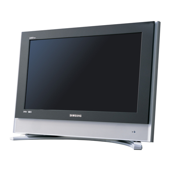
Samsung LW22N23N Service Manual
Tft-lcd tv/monitor
Hide thumbs
Also See for LW22N23N:
- Connecting manual (4 pages) ,
- Owner's instructions manual (68 pages) ,
- Service manual (27 pages)
Advertisement
Quick Links
SERVICE
TFT-LCD TV/MONITOR
All manuals and user guides at all-guides.com
TFT-LCD TV/MONITOR
Chassis
VR22EO
Model
LW22N23N
Manual
CONTENTS
1. Precautions
2. Product Specifications
3. Disassembly & Reassembly
4. Alignment & Adjustments
5. Troubleshooting
6. Exploded View & Parts List
7. Parts List
8. Block Diagram
9. Wiring Diagram
10. PCB Layout
11. Schematic Diagrams
12. Panel Description
Advertisement

Related Manuals for Samsung LW22N23N


Summary of Contents for Samsung LW22N23N
- Page 1 All manuals and user guides at all-guides.com TFT-LCD TV/MONITOR Chassis Model VR22EO LW22N23N SERVICE Manual TFT-LCD TV/MONITOR CONTENTS 1. Precautions 2. Product Specifications 3. Disassembly & Reassembly 4. Alignment & Adjustments 5. Troubleshooting 6. Exploded View & Parts List 7. Parts List 8.
- Page 2 6. Do not attempt to connect or disconnect any wire while the TV is turned on. Make sure that the power cord is disconnected before replacing any parts. 7. To protect aganist shock hazard, use an isolation transform. LW22N23N...
- Page 3 1. Remote - Control Key : Power, Arrow Up, Arrow Down, Arrow Left Arrow Right, Menu, Enter, Number Key(0~9) 2. Function - Control Key : Power, CH +, CH -, VOL +, VOL -, Menu, TV/VIDEO(Enter) 4-2-2 Factory Mode Tree LW22N23N...
- Page 4 All manuals and user guides at all-guides.com 4 Alignments and Adjustments LW22N23N...
- Page 5 All manuals and user guides at all-guides.com 4 Alignments and Adjustments LW22N23N...
- Page 6 All manuals and user guides at all-guides.com 4 Alignments and Adjustments LW22N23N...
- Page 7 All manuals and user guides at all-guides.com 4 Alignments and Adjustments LW22N23N...
- Page 8 All manuals and user guides at all-guides.com 4 Alignments and Adjustments LW22N23N...
- Page 9 All manuals and user guides at all-guides.com 4 Alignments and Adjustments * Unless otherwise specifid, do not adjust data in Factory Mode. * Data may be changed for display improvement. LW22N23N...
-
Page 10: White Balance Adjustment
4. As the RF mode is applied with the same vlaues as for VIDEO and S-VIDEO, adjustment can be made in any of RF, VIDEO and S-VIDEO modes. Table 4-1. White Balance Setting Conditions Table 4-2. Color Control Default Vlaue Table 4-3. Color Control Default Vlaue LW22N23N... -
Page 11: Method Of Adjustment
Set the input to the mode in which the adjustment will be made (RF PC). * Input signal - VIDEO Mode : Model #1 (750*480 Mode), Pattern #16 - PC Mode : Model #21 (1024*768 Mode), Pattern #16 b) Enter factory color control, confirm the data. 4-10 LW22N23N... - Page 12 Adjust the high light. (Refer to table 1, 2 in adjustment position by mode) - Adjust red gain ('x') and blue gain ('y') to the color coordinates. * Do not adjust the green gain and sub-contrast (Y) data. Picture 4-3 Toshiba ABL Pattern High light Measurement point LW22N23N 4-11...
-
Page 13: Option Table
4 Alignments and Adjustments 4-3-3 Option Table * The default settings are most recommended for Option Data. Each data may be adjusted. 4-3-4 PW565 * Below figures are for contrast adjustment of PW565 (IC565). Do not change the data. 4-12 LW22N23N... - Page 14 All manuals and user guides at all-guides.com 4 Alignments and Adjustments 4-3-5 VPC 3230-MAIN * Data may be adjusted. 4-3-6 ADC *Adjust the R(Pr), G(Y), B(Pb) gain and offset to the basic level of DTV and PC Input signals. LW22N23N 4-13...
-
Page 15: Test Pattern
(Varies depending on program update) 4-3-11 Reset * Initializes the data in the MICOM. (Set to default value) Use ‘Reset’ to restore adjustmints made in Factory Mode to the original settings. 4-3-12 T_VIC22NUS_0166 11/27/2003 20:10:51 * Displays the MICOM program version 4-14 LW22N23N... - Page 16 3. After completing the JIG Cable connection, store Update practice program (hex file 3EA) in new folder. (guiR, romcode, factoryGui). 4. Click FlashupgradNT.exe icon 2 times and execute it. (Upgrader OSD screen is marked) Picture 4-4 5. Select OFull.inf in Flash. (flaher, romcode, guir, factorygui items look in Files To) Picture 4-5 LW22N23N 4-15...
- Page 17 (Connect only when you want to see PC screen.) 2. Connect with JIG Output (15 pins) and PC Input (PC/DVI 24 pins) terminal. 3. Connect with COM Port1 of PC (9 Pins). 4. Connect 14V 4.5A Adaptor Cable. 4-16 LW22N23N...
-
Page 18: Block Diagram
All manuals and user guides at all-guides.com 8 Block Diagram ❈ This Document can not be used without Samsung’s authorization. LW22N23N... - Page 19 9 Wiring Diagram KEY1 CN804 POWER_KEY CH+_OUT CH-_OUT SOURCE_OUT CN505 IDENT_HP CN803 HP_L HP_R ADJ_BRIGHT PC_AUDIO_L SW_INVERTER CN601 PC_AUDIO_R S_VHS_C S_VHS_Y VIDEO_CVBS VIDEO_L VIDEO_R LED_GRN CN806 LED_RED A3.3V CN801 CN809 SPKOUT R+ CN701 SPKOUT R- CN808 SPKOUT L+ CN702 SPKOUT L- LW22N23N...
- Page 20 All manuals and user guides at all-guides.com 11 Schematic Diagrams ❈ This Document can not be used without Samsung’s authorization. 11-5 SOUND PROCESSOR, SOUND AMP, POWER Schematic Diagram SW_POWER_1 TP601 SUPLVAL TP602 TP628 TP623 C601 SUPLVAL SUPLVAL TP603 10nF L602...
- Page 21 All manuals and user guides at all-guides.com 11 Schematic Diagrams The Signal are Inputed to IC703 DC +8V Output WaveForm 11-6 LW22N23N...
- Page 22 All manuals and user guides at all-guides.com 11 Schematic Diagrams ❈ This Document can not be used without Samsung’s authorization. 11-6 INPUT CONECTOR Schematic Diagram L902 R801 DUAL SCART JACK 3.3UH 1/8W FT803 (3722-001991) CN808 C845 C846 TMQZ6-406A 470uF 100nF...
- Page 23 All manuals and user guides at all-guides.com 11 Schematic Diagrams ❈ This Document can not be used without Samsung’s authorization. 11-1 VIDEO DECORDER ADC, SWITCH Schematic Diagram R,G,B Output Signal (#15,19,21) Of IC102 3.3V BD201 MDIN150I(0:15) BLM41P600S C202 C203 C201...
- Page 24 All manuals and user guides at all-guides.com 11 Schematic Diagrams ❈ This Document can not be used without Samsung’s authorization. 11-2 DVE, DNI 3D Comb Schematic Diagram 3.3V 3.3V Output Digital Signal of IC403 FT401 FT402 SGM32F1E104-2A SGM32F1E104-2A RA308 IPDATACH1A(0:23)
- Page 25 All manuals and user guides at all-guides.com 11 Schematic Diagrams ❈ This Document can not be used without Samsung’s authorization. 11-3 PW565_Scaler LVDS, Video_Memory, Flash_Memory Schematic Diagram Output Digital Signal of IC565 3.3V A3.3V FSADDR(11) FSADDR(11) FSADDR(12) FSADDR(12) FSADDR(10) FSADDR(10) FSADDR(0) A3.3V...
- Page 26 All manuals and user guides at all-guides.com 11 Schematic Diagrams ❈ This Document can not be used without Samsung’s authorization. 11-4 CAPTION, TTX DEINTERLACER, SUB_MICOM Schematic Diagram Digital Output Y,C_OUT (0:7) Data Of IC405 3.3V +3.3V_MD C914 100nF C913 FT406...
- Page 27 All manuals and user guides at all-guides.com www.s-manuals.com...