Table of Contents
Advertisement
Quick Links
SERVICE MANUAL
System
Laser: Semiconductor laser
Signal format system: NTSC/PAL
Audio characteristics
Frequency response: DVD VIDEO (PCM
96 kHz): 2 Hz to 44 kHz (±1.0 dB)/DVD
VIDEO (PCM 48 kHz): 2 Hz to 22 kHz
(±0.5 dB)/CD: 2 Hz to 20 kHz (±0.5 dB)
Signal-to-noise ratio (S/N ratio): 115 dB
(LINE OUT (L/R) AUDIO jacks only)
Harmonic distortion: 0.003 %
Dynamic range: DVD VIDEO: 103 dB/CD:
99 dB
Wow and flutter: Less than detected value
(±0.001% W PEAK)
The signals from LINE OUT L/R (AUDIO)
jacks are measured. When you play PCM
sound tracks with a 96 kHz sampling
frequency, the output signals from the
DIGITAL OUT ( COAXIAL) jack are
converted to 48 kHz sampling frequency.
SPECIFICATIONS
Outputs/Inputs
(Jack name: Jack type/Output or Input level/
Load impedance)
LINE OUT (AUDIO): Phono jack/2 Vrms/
10 kilohms
DIGITAL OUT (COAXIAL): Phono jack/
0.5 Vp-p/75 ohms
COMPONENT VIDEO OUT
(Y, P
, P
):
B
R
Phono jack/Y: 1.0 Vp-p/P
, P
B
0.65 Vp-p/75 ohms
(Y, P
/C
, P
/C
):
B
B
R
R
Phono jack/Y: 1.0 Vp-p/
P
/C , P
B
0.7 Vp-p/75 ohms
LINE OUT (VIDEO): Phono jack/1.0 Vp-p/
75 ohms
S VIDEO OUT: 4-pin mini DIN/Y:
1.0 Vp-p, C: 0.286 Vp-p (NTSC)/
75 ohms
1.0 Vp-p, C: 0.3 Vp-p (PAL)/75 ohms
XD-AX10
RM-Z400A/Z400E
Canadian Model
Singapore Model
Middle East Model
Australian Model
New Zealand Model
Hong Kong Model
Saudi Arabia Model
Russian Model
General
Power requirements:
120 V AC, 60 Hz
110 to 240 V AC, 50/60 Hz
220 to 240 V AC, 50/60 Hz
See page 1-1 for further information.
Power consumption: 13 W
Dimensions (approx.): 430 ×55.5 ×
234 mm (17 × 2
:
height/depth) incl. projecting parts
R
Mass (approx.): 2.2 kg (4 lb 14 oz)
Operating temperature: 5 °C to 35 °C
°
/C :
(41
F to 95
B
R
R
Operating humidity: 25 % to 80 %
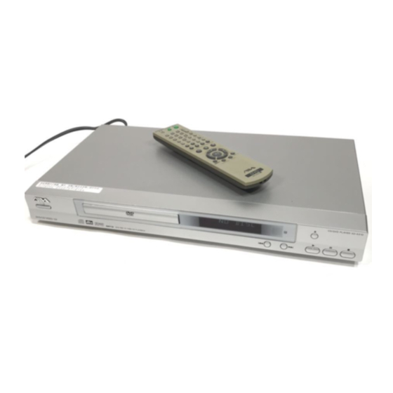
Supplied accessories
Check that you have the following items:
• Audio/video cord
(pinplug × 3 y pinplug × 3) (1)
• Remote commander (remote) (1)
• Size AA (R6) batteries (2)
• A plug adaptor is included with some
models.
Specifications and design are subject to
change without notice.
CD/DVD PLAYER
AEP Model
UK Model
E Model
× 9
in.) (width/
3
/
1
/
16
4
°
F)
Advertisement
Table of Contents
Troubleshooting

Related Manuals for Sony XD-AX10


Summary of Contents for Sony XD-AX10
- Page 1 XD-AX10 RM-Z400A/Z400E SERVICE MANUAL Canadian Model AEP Model UK Model E Model Singapore Model Middle East Model Australian Model New Zealand Model Hong Kong Model Saudi Arabia Model Russian Model SPECIFICATIONS System Outputs/Inputs General Laser: Semiconductor laser (Jack name: Jack type/Output or Input level/...
- Page 2 OPERATION. REPLACE THESE COMPONENTS WITH DE FONCTIONNEMENT. NE REMPLACER CES COM- SONY PARTS WHOSE PART NUMBERS APPEAR AS POSANTS QUE PAR DES PIÈCES SONY DONT LES SHOWN IN THIS MANUAL OR IN SUPPLEMENTS PUB- NUMÉROS SONT DONNÉS DANS CE MANUEL OU LISHED BY SONY.
-
Page 3: Table Of Contents
TABLE OF CONTENTS Section Title Page Section Title Page SERVICE NOTE DISASSEMBLY Disc Removal Procedure (at POWER OFF) ....5 2-1. Disassembly ..............2-1 How to Service MB-108 Board ........5 2-2. Upper Case ..............2-1 2-3. Tray Cover ..............2-2 2-4. -
Page 4: Section Title Page
Section Title Page IC PIN FUNCTION DESCRIPTION 5-1. System Control Pin Function (MB-108 BOARD IC104) .......... 5-1 TEST MODE 6-1. General Description ............6-1 6-2. Starting Test Mode ............6-1 6-3. Syscon Diagnosis ............6-1 6-4. Drive Auto Adjustment ..........6-6 6-5. -
Page 5: Service Note
SERVICE NOTE 1. DISC REMOVAL PROCEDURE (at POWER OFF) 1) Open dust cover to access to a hole insert a tapering driver into the aperture of the unit bottom, and move the lever of chuck cam in the direction of arrow A. (See Fig. 1) 2) Draw out the tray in the direction of arrow B, and remove a disc. - Page 6 4) Set the board in the place where the MB-108 board is removed, as shown in Fig. 4. Flexible flat cable (FMS-23: CN105) Flexible flat cable (FMO-8: CN103) Flexible flat cable (FMM-48: CN101) Screw (B3) CK-120 board Connector (CN109) Connector (CN113) Two screws Screw...
-
Page 7: General
XD-AX10 SECTION 1 This section is extracted from instruction GENERAL manual (3-081-707-11). For the model supplied with the AC plug Precautions About This Manual This Player Can Play the adaptor If the AC plug of your unit does not fit into... -
Page 8: Index To Parts And Controls
Front panel display Index to Parts and Controls When playing back a DVD For more information, refer to the pages indicated in parentheses. Playing status Lights up when you can change the angle (45) Disc type Front panel Current title/chapter or playing Lights up during Current audio signal (41) Repeat Play (34) -
Page 9: Guide To On-Screen Displays (Control Bar)
◆Display 2 ◆No display Displaying the Control Bar in Guide to On-Screen The following playback information is stop mode displayed. Displays (Control Bar) Example: When playing a DVD ◆Return to Display 1 The following displays appear when the DISPLAY button is repeatedly pressed The following explains the Control Bar. -
Page 10: Step 4: Connecting The Audio Cords
B If you are connecting to an S VIDEO input jack Step 4: Connecting the Audio Cords Connect the S VIDEO cord (not supplied). You will enjoy high quality images. Refer to the chart below to select the connection that best suits your system. Be sure to also read the instructions for the components you wish to connect. -
Page 11: Step 5: Connecting The Power Cord
Connecting to an AV amplifier (receiver) having a Dolby Surround (Pro Connecting to an AV amplifier (receiver) with a digital input jack having Logic) decoder and 3 to 6 speakers a Dolby Digital or DTS decoder and 6 speakers You can enjoy the Dolby Surround effects only when playing Dolby Surround audio or multi- This connection will allow you to use the Dolby Digital or DTS decoder function of your AV channel audio (Dolby Digital) discs. -
Page 12: Playing Discs
Press A on the player, and place a • Do not play DTS sound tracks without first Operation connecting the player to an audio disc on the disc tray. Stop play and remove Press Z component having a built-in DTS decoder. Playing Discs the disc The player outputs the DTS signal via the... -
Page 13: Playing Video Cds With Pbc Functions (Pbc Playback)
z Hint Playing VIDEO CDs with To play without using PBC, press ./> or the Playing an MP3 Audio 1 ( 3 0 ) number buttons while the player is stopped to select R O C K B E S T H I T PBC Functions Track a track, then press H or ENTER. -
Page 14: Searching For A Scene
Press C/c to select (SHUFFLE), Next, press X/x or the number buttons to Follow Step 4 for new programming. To Playing repeatedly (Repeat Play) select “03” under “C,” then press cancel a program, select “--” under “T,” then press ENTER repeatedly to select ENTER. -
Page 15: Searching For A Title/Chapter/Track/Scene, Etc
Press SEARCH MODE repeatedly Playing one frame at a time Notes Searching for a Title/ to select the search method. (Freeze Frame) • You cannot search for a scene on a DVD+RW Chapter/Track/Scene, ◆ When playing a DVD using the time code. When the player is in the pause mode, press •... -
Page 16: Sound Adjustments
Press AUDIO repeatedly to select About audio signals Virtual Surround Settings Audio signals recorded in a disc contain the the desired audio signal. sound elements (channels) shown below. Sound Adjustments ◆ When playing a DVD Each channel is output from a separate Changing the Sound Depending on the DVD, the choice of speaker. -
Page 17: Changing The Angles
Press X/x to select (PARENTAL Changing the Angles CONTROL), then press ENTER. Locking Discs The options for “PARENTAL CONTROL” appear. If various angles (multi-angles) for a scene Limiting Playback by are recorded on the DVD, “ ” appears in the front panel display. -
Page 18: Settings And Adjustments
Press X/x to select “CUSTOM,” Select a setting using X/x, then Setting the Display or then press ENTER. press ENTER. Settings and Adjustments Sound Track Language The Setup Display appears. The setting is selected and setup is complete. Using the Setup Display LANGUAGE SETUP (LANGUAGE SETUP) Example: “16:9”... -
Page 19: Settings For The Sound (Audio Setup)
◆ PAUSE MODE (DVD only) ◆ DOWNMIX (DVD only) If you connect a component that does not Settings for the Sound conform to the selected audio signal, a loud Selects the picture in pause mode. Switches the method for mixing down to 2 noise (or no sound) will come out from the channels when you play a DVD which has AUTO... -
Page 20: Glossary
The picture data uses the MPEG 2 format, one The disc tray does not open and “LOCKED” Self-diagnosis Function Glossary of the worldwide standards of digital appears on the front panel display. compression technology. The picture data is , Child Lock is set (page 26). compressed to about 1/40 (average) of its (When letters/numbers appear in the Chapter (page 10) -
Page 21: Disassembly
XD-AX10 SECTION 2 DISASSEMBLY 2-1. DISASSEMBLY • This set can be disassembled in the order shown below. Upper case (Page 2-1) Tray cover MB-108 board (Page 2-2) (Page 2-4) Front panel section (Page 2-2) Mechanism deck Power block AF-98 board... -
Page 22: Tray Cover
2-3. TRAY COVER 1 Open the dust cover. 5 Tray cover 2 Slide the lever. 4 Two claws 3 Draw out the tray. 2-4. FRONT PANEL SECTION 5 Claw 4 Claw 1 Flexible flat cable (FFS-10: CN402) 6 Front panel section 3 Claw 2 Claw... -
Page 23: Mechanism Deck
2-5. MECHANISM DECK 5 Three screws (B3) 1 Connector (CN201) 6 Mechanism deck 2 Connector (CN471) 3 Two flexible flat cables (FMM-48: CN203/FMO-8: CN204) 4 Flexible flat cable (FMS-23: CN201) 2-6. OPTICAL PICK-UP 6 Insulator 3 Insulator screw 4 Insulator 7 Optical pick-up 5 Insulator 1 Insulator screw... -
Page 24: Board (Aep, Uk, Russian)
2-7. ER-21 BOARD (AEP, UK, RUSSIAN) 3 ER-21 board 1 Flexible flat cable (FAE-11: CN901) 2 Two screws (B3) 2-8. MB-108 BOARD 2 Flexible flat cable (FMS-23: CN201) 1 Two flexible flat cables (FMM-48: CN203/FMO-8: CN204) 6 Three screws (B3) 3 Connector 5 Connector (CN102) -
Page 25: Power Block
2-9. POWER BLOCK 3 Four screws 1 Connector (B3) (CN101) 2 Connector (CN201) 4 Power block 2-10. AF-98 BOARD 2 Connector (CN471) 4 Two screws 1 Flexible flat cable (B3) (FAE-11: CN102) 5 AF-98 board 3 Six screws (B3) -
Page 26: Internal Views
2-11. INTERNAL VIEWS — Top view — — Bottom view — M001 Loading motor 1-763-967-11 Optical pick-up (KHM-290AAA) A-6061-908-A... -
Page 27: Circuit Boards Location
2-12. CIRCUIT BOARDS LOCATION Power supply block (HS8S2U) (Canadian) (ETXNY410M0F) (E, Saudi Arabia, Hong Kong, Singapore, Australian, Middle East) (ETXNY410E0F) (AEP, UK, Russian) ER-21 board (EURO AV) (AEP, UK, Russian) AF-98 board (INTERFACE CONTROL AUDIO/VIDEO OUT) MS-128 board (LOADING MOTOR) MB-108 board (SIGNAL PROCESS SERVO) SW-384 board... -
Page 28: Block Diagrams
XD-AX10 SECTION 3 BLOCK DIAGRAMS 3-1. OVERALL BLOCK DIAGRAM AEP, UK, RUS ER-21 BOARD (SEE PAGE 4-35, 36) CNJ902 IC901 LINE 1 VIDEO BUFFER (RGB)-TV SELECT SWITCH AC IN AF-98 BOARD J104(2/2) (SEE PAGE 4-23 to 4-30) LINE OUT VIDEO •... -
Page 29: Rf/Servo Block Diagram
XD-AX10 3-2. RF/SERVO BLOCK DIAGRAM IC201 tl IC201 (CD PB) IC201 2 (DVD PLAY) IC201 rs (CD PB) IC201 rs (DVD PLAY) 890nsec 1.3Vp-p 20nsec 0.47Vp-p 20nsec 0.79Vp-p 383mVp-p 433mVp-p BASE UNIT MB-108 BOARD (1/4) KHM-290AAA/SERVICE ASSY IC301 (CD PB) -
Page 30: Signal Processor Block Diagram
XD-AX10 3-3. SIGNAL PROCESSOR BLOCK DIAGRAM MB-108 BOARD (2/4) (SEE PAGE 4-13 to 4-16) ∗ IC405: EXCEPT CND, E ∗ IC404, 405 16M SDRAM IC301 <zzz (DVD PLAY) IC303 • Abbreviation : Canadian model 16M DRAM 1.34Vp-p 40ns/div IC301 <zzc (CD PB) 105 –... -
Page 31: System Control Block Diagram
XD-AX10 3-4. SYSTEM CONTROL BLOCK DIAGRAM MB-108 BOARD (3/4) (SEE PAGE 4-9, 10) IC106 IC107 32M FLASH HA 0 – 21 HA 0 – 21 HD 0 – 15 HD 0 – 15 IC104 tf 1 – 5 102 – 109 111 – 118 120 85 – 100 59 72 84 HA 0 –... -
Page 32: Video Block Diagram
XD-AX10 3-5. VIDEO BLOCK DIAGRAM • Abbreviation IC102 ed : Russian model AF-98 (1/3) (SEE PAGE 4-23, 24) IC102 VIDEO BUFFER J104 (1/2) 2.5Vp-p CN203 (1/2) VIDEO IN VIDEO OUT VIDEO LINE OUT IC102 wl J103 Y IN Y OUT... -
Page 33: Audio Block Diagram
XD-AX10 3-6. AUDIO BLOCK DIAGRAM AF-98 BOARD (2/3) (SEE PAGE 4-25, 26) MB-108 BOARD (4/4) (SEE PAGE 4-17, 18) CN601 (3/3) CN203 (2/2) J201 SPDIF Q211 SPDIF DIGITAL BUFFER COAXIAL IC601 IC601 IC201 SIGNAL PROCESSOR AUDIO D/A CONVERTER (SEE PAGE 3-6) AUDIO AMP 3.3Vp-p... -
Page 34: Interface Control Block Diagram
XD-AX10 3-7. INTERFACE CONTROL BLOCK DIAGRAM AF-98 BOARD (3/3) (SEE PAGE 4-29, 30) CN401 SYSTEM CONTROL XIFCS XIFCS (SEE PAGE 3-8) XIFBUSY XIFBUSY BUSY SW-348 BOARD XFRRST (SEE PAGE 4-32) XFRRST /FRRST IC820 REMOTE COMMANDER RECEIVER AUDIO A MUTE /AMUTE... -
Page 35: Power 1 Block Diagram
XD-AX10 3-8. POWER 1 BLOCK DIAGRAM POWER SUPPLY BLOCK (HS8S2U): (CND) (SEE PAGE 4-39, 40) T101 D221 L221 EVER+11V POWER TRANSFORMER Q211 D211 L211 SW+11V Q311 P311 D311 L311 SW+5V CN101 AC IN D101 F101 L101 LINE FILTER Q611 P611... -
Page 36: Power 2 Block Diagram
XD-AX10 3-9. POWER 2 BLOCK DIAGRAM POWER SUPPLY BLOCK (ETXNY410M0F): (E, SP, ME, AUS, HK, EA) (SEE PAGE 4-43, 44) (ETXNY410E0F): (AEP, UK, RUS) (SEE PAGE 4-47, 48) CN201 Q301 L301 D301 SW+11V T101 L205 D201 L201 EVER+11V Q203 D202... -
Page 37: Power 3 Block Diagram
XD-AX10 3-10. POWER 3 BLOCK DIAGRAM AEP, UK, RUS AF-98 BOARD (SEE PAGE 4-23 to 4-30) ER-21 BOARD (SEE PAGE 4-35, 36) CN471 PS472 EVER+11V CN102 CN901 IC901 +11V +11V VIDEO BUFFER Q472, 473 PS471 SELECT EVER-15.5V IC103 SWITCH -5V REG... -
Page 38: Frame Schematic Diagram
XD-AX10 SECTION 4 PRINTED WIRING BOARDS AND SCHEMATIC DIAGRAMS THIS NOTE IS COMMON FOR PRINTED WIRING For schematic diagram: • Caution when replacing chip parts. BOARDS AND SCHEMATIC DIAGRAMS. New parts must be attached after removal of chip. (In addition to this, the necessary note is printed... - Page 39 XD-AX10 4-1. FRAME SCHEMATIC DIAGRAM AEP, UK, RUS BASE UNIT KHM-290AA/SERVICE ASSY POWER SUPPLY CN203 25P CN601 25P CN203 26P Cr/B_Cr/R Cr/B_Cr/R BLOCK Cb/R_Cb/B Cb/R_Cb/B HS8S2U : CND ETXNY410E0F: AEP, UK, RUS ETXNY410M0F : E, SP, ME, AUS, HK, EA...
-
Page 40: Printed Wiring Board
XD-AX10 4-2. PRINTED WIRING BOARDS AND SCHEMATIC DIAGRAMS There are a few cases that the part isn't mounted in this model is printed on this diagram. MB-108 (SIGNAL PROCESS, SERVO) PRINTED WIRING BOARD – Ref. No.: MB-108 board; 1,000 series –... - Page 41 XD-AX10 MB-108 BOARD (SIDE B) MB-108 BOARD(SIDE B) IC101 IC103 IC505 IC107 IC201 IC202 IC303 R577 IC503 IC401 C538 C518 IC404 R417 C243 Q202 IC405 R436 R416 C602 L202 C429 Q201 C415 IC406 Q202 C439 R522 JL505 R526 FL403 R589...
- Page 42 XD-AX10 MB-108 (SYSTEM CONTROL) SCHEMATIC DIAGRAM • See page 4-5 for printed wiring board, and see page 4-49 for waveforms. – Ref. No.: MB-108 board; 1,000 series – MB-108 BOARD (1/5) MB-108 BOARD (2/5 – 4/5) SYSTEM CONTROL MB-108 BOARD -REF.NO.:1000 SERIES-...
-
Page 43: Rf Amp, Servo Error Process) Schematic Diagram
XD-AX10 MB-108 (RF AMP, SERVO ERROR PROCESS) SCHEMATIC DIAGRAM The components identified by mark 0 or dotted Les composants identifiés par une marque 0 sont line with mark 0 are critical for safety. critiques pour la sécurité. Ne les remplacer que •... -
Page 44: Arp, Servo Dsp) Schematic Diagram
XD-AX10 MB-108 (ARP, SERVO DSP) SCHEMATIC DIAGRAM • See page 4-5 for printed wiring board, and see page 4-49 for waveforms. – Ref. No.: MB-108 board; 1,000 series – MB-108 BOARD (3/5) ARP, SERVO DSP -REF.NO.:1000 SERIES- XX MARK:NO MOUNT... -
Page 45: Av Decoder) Schematic Diagram
XD-AX10 MB-108 (AV DECODER) SCHEMATIC DIAGRAM • See page 4-5 for printed wiring board, and see page 4-49 for waveforms. – Ref. No.: MB-108 board; 1,000 series – MB-108 BOARD (4/5) AV DECODER -REF.NO.:1000 SERIES- XX MARK:NO MOUNT NO MARK:PB MODE... -
Page 46: Audio D/A Converter
XD-AX10 MB-108 (AUDIO D/A CONVERTER) SCHEMATIC DIAGRAM • See page 4-5 for printed wiring board, and see page 4-49 for waveforms. – Ref. No.: MB-108 board; 1,000 series – MB-108 BOARD (5/5) AUDIO D/A CONVERTER -REF.NO.:1000 SERIES- XX MARK:NO MOUNT... -
Page 47: Schematic Diagram
XD-AX10 MS-128 (LOADING MOTOR) PRINTED WIRING BOARD AND SCHEMATIC DIAGRAM – Ref. No.: MS-128 board; 1,000 series – : Uses unleaded solder. There are a few cases that the part isn't mounted in this model is printed on this diagram. - Page 48 XD-AX10 COMPONENT AF-98 (INTERFACE CONTROL AUDIO/VIDEO OUT) PRINTED WIRING BOARD DIGITAL OUT LINE OUT VIDEO OUT COAXIAL AUDIO VIDEO – Ref. No.: AF-98 board; 2,000 series – S VIDEO AF-98 BOARD : Uses unleaded solder. J104 J201 J103 JL204 J102...
-
Page 49: Video Out) Schematic Diagram
XD-AX10 AF-98 (VIDEO OUT) SCHEMATIC DIAGRAM • See page 4-21 for printed wiring board, and see page 4-49 for waveforms. – Ref. No.: AF-98 board; 2,000 series – AF-98 BOARD (1/4) VIDEO OUT -REF.NO.:2000 SERIES- XX MARK:NO MOUNT IC102 NO MARK:PB MODE... -
Page 50: Audio Out) Schematic Diagram
XD-AX10 AF-98 (AUDIO OUT) SCHEMATIC DIAGRAM • See page 4-21 for printed wiring board. – Ref. No.: AF-98 board; 2,000 series – AF-98 BOARD (2/4) 4700 AUDIO OUT -REF.NO.:2000 SERIES- 5600 XX MARK:NO MOUNT 4700 5600 180p NO MARK:PB MODE... -
Page 51: Regulator) Schematic Diagram
XD-AX10 AF-98 (REGULATOR) SCHEMATIC DIAGRAM • See page 4-21 for printed wiring board. – Ref. No.: AF-98 board; 2,000 series – AF-98 BOARD (3/4) REGULATOR -REF.NO.:2000 SERIES- XX MARK:NO MOUNT NO MARK:PB MODE MARKED:MOUNT TABLE IC473 +1.8V REG AF-98 BOARD (4/4) AF-98 BOARD (2/4, 4/4) -15.2... -
Page 52: If Con) Schematic Diagram
XD-AX10 AF-98 (IF CON) SCHEMATIC DIAGRAM • See page 4-21 for printed wiring board, and see page 4-49 for waveforms. – Ref. No.: AF-98 board; 2,000 series – MB-108 BOARD (1/5) MB-108 BOARD (1/5) CN102 CN101 AF-98 BOARD (4/4) (SEE PAGE 4-10) -
Page 53: Function Switch) Schematic Diagram
XD-AX10 SW-384 (FUNCTION SWITCH) SCHEMATIC DIAGRAM – Ref. No.: SW-384 board; 1,000 series – SW-384 BOARD XX MARK:NO MOUNT NO MARK:DVD/CD PLAY R812 R807 2700 S811 JS812 S808 JS813 JS815 JS814 S809 CN801 R805 R803 R802 R804 +3.3V AF-98 BOARD (4/4) - Page 54 XD-AX10 ER-21 (EURO AV) PRINTED WIRING BOARD There are a few cases that the part isn't mounted in this model is printed on this diagram. – Ref. No.: ER-21 board; 9,000 series – – AEP, UK, RUS – LINE (RGB) -TV : Uses unleaded solder.
-
Page 55: Euro Av) Schematic Diagram
XD-AX10 ER-21 (EURO AV) SCHEMATIC DIAGRAM – Ref. No.: ER-21 board; 9,000 series – – AEP, UK, RUS – ER-21 BOARD (AEP, UK, RUS) EURO AV -REF.NO.:9000 SERIES- VIDEO SIGNAL AUDIO XX MARK:NO MOUNT SIGNAL CHROMA Y/CHROMA NO MARK:PB MODE... -
Page 56: Power Supply Block (Hs8S2U) Printed Wiring Board
XD-AX10 POWER SUPPLY BLOCK (HS8S2U) PRINTED WIRING BOARD – Ref. No.: HS8S2U board; 1,000 series – – CND – : Uses unleaded solder. There are a few cases that the part isn't mounted in this model is printed on this diagram. -
Page 57: Power Supply Block (Hs8S2U) Schematic Diagram
XD-AX10 POWER SUPPLY BLOCK (HS8S2U) SCHEMATIC DIAGRAM – Ref. No.: HS8S2U board; 1,000 series – – CND – POWER SUPPLY BLOCK (CND) (HS8S2U) -REF.NO.:1000 SERIES- XX MARK:NO MOUNT NO MARK:REC/PB MODE Q211 2SJ525 B+ SWITCH SW201 POWER SW IC101 AF-98 BOARD... -
Page 58: Power Supply Block (Etxny410M0F) Printed Wiring Board
XD-AX10 POWER SUPPLY BLOCK (ETXNY410M0F) PRINTED WIRING BOARD – Ref. No.: ETXNY410M0F board; 5,000 series – – E, SP, ME, AUS, HK, EA – : Uses unleaded solder. There are a few cases that the part isn't mounted in this model is printed on this diagram. -
Page 59: Power Supply Block (Etxny410M0F) Schematic Diagram
XD-AX10 POWER SUPPLY BLOCK (ETXNY410M0F) SCHEMATIC DIAGRAM – Ref. No.: ETXNY410M0F board; 5,000 series – – E, SP, ME, AUS, HK, EA – POWER SUPPLY BLOCK (E, SP, ME, AUS, HK, EA) (ETXNY410M0F) -REF.NO.:5000 SERIES- XX MARK:NO MOUNT NO MARK:PB MODE... -
Page 60: Power Supply Block (Etxny410E0F) Printed Wiring Board
XD-AX10 POWER SUPPLY BLOCK (ETXNY410E0F) PRINTED WIRING BOARD – Ref. No.: ETXNY410E0F board; 3,000 series – – AEP, UK, RUS – : Uses unleaded solder. There are a few cases that the part isn't mounted in this model is printed on this diagram. -
Page 61: Power Supply Block (Etxny410E0F) Schematic Diagram
XD-AX10 POWER SUPPLY BLOCK (ETXNY410E0F) SCHEMATIC DIAGRAM – Ref. No.: ETXNY410E0F board; 3,000 series – – AEP, UK, RUS – POWER SUPPLY BLOCK (AEP, UK, RUS) (ETXNY410E0F) -REF.NO.:3000 SERIES- XX MARK:NO MOUNT NO MARK:PB MODE B+ SWITCH 250V EVER+11V B+ SWITCH... -
Page 62: Waveforms
XD-AX10 • Waveforms AF-98 BOARD MB-108 BOARD IC102 ed IC103 3 IC201 ra (DVD PLAY) IC301 (CD PB) IC403 yd 2.5Vp-p 1.7Vp-p 770mVp-p 3.3Vp-p 625mVp-p 1.17msec 21msec 6.8usec IC102 ea IC103 8 IC201 rs (CD PB) IC301 (DVD PLAY) IC403 yg 2.0Vp-p... - Page 63 XD-AX10 SECTION 5 IC PIN FUNCTION DESCRIPTION...
- Page 64 5-2 E...
-
Page 65: Test Mode
XD-AX10 SECTION 6 TEST MODE 6-1. GENERAL DESCRIPTION 6-3. SYSCON DIAGNOSIS The Test Mode allows you to make diagnosis and adjustment eas- The same contents as board detail check by serial interface can be ily using the remote commander and monitor TV. The instructions, checked from the remote commander. - Page 66 * In "All item continuous check", pressing stop or enter will not (2-6) M't check quit the diagnosis. Mount resistance is checked. Error 22: The region code does not accord. Selecting 2 and subsequent items calls the submenu screen of Check wether the region code that is deduced from model each item.
- Page 67 5. Data Supply System (5-5) ARP RAM Check Data write → read, and accord check (5-2) ARP Register Check Data write → read, and accord check Error 11: ARP RAM read data discord Error 08: ARP register write, and read data discord The program code data stored in ROM are copied to all Data 0x00 to 0xFF is written sequentially to the ARP TMAX areas of RAM (IC303) connected to the ARP (IC301)
- Page 68 7. Video Output Diagnosis Check Items List (7-2) Color Bar AVD color bar command write → Video OUT 2) Version Error: Not detected. (2-2) Revision The command is transferred to the AVD, and the color bar (2-3) ROM Check Sum signals are output from video terminals.
- Page 69 Error Codes List 00: Error not detected 01: RAM write/read data discord 03: EEPROM NG 04: Flash memory clear error 05: Flash memory write error 06: Flash memory read data discord 08: ARP register read data discord 09: ARP ←→ RAM data bus error 10: ARP ←→...
-
Page 70: Drive Auto Adjustment
1. DVD Single Layer Disc 6-4. DRIVE AUTO ADJUSTMENT [ENTER] Select , insert DVD single layer disc, and press key, and the adjustment will be made through the following steps, then DVD reference disc adjusted values will be written to the EEPROM. Single Layer HLX-503 (J-6090-069-A) (NTSC) DVD Single Layer Disc Adjustment Steps... - Page 71 2. CD 3. DVD Dual Layer Disc [ENTER] [ENTER] Select , insert CD disc, and press key, and the adjust- Select , insert DVD dual layer disc, and press key, ment will be made through the following steps, then adjusted val- and the adjustment will be made through the following steps, then ues will be written to the EEPROM.
-
Page 72: Drive Manual Operation
0. Disc Check Memory 6-5. DRIVE MANUAL OPERATION Disc Check On the Test Mode Menu screen, select , and the manual opera- tion menu will be displayed. For the manual operation, each servo on/off control and adjustment can be executed manually. 1. - Page 73 Focus : Search the focus and turn on the focus. Disc Type 1. Disc Type Auto Check : Turn ON/OFF the tracking servo. 2. DVD SL 12cm 3. DVD DL 12cm 4. CD 12cm Sled : Turn ON/OFF the sled servo. 5.
- Page 74 ← Fj (L0 → L1) 5. Auto Adjustment : Focus jump reverse. (Trk/Sled Servo OFF) Auto Adjustment ↑ Lj (L1 → L0) : Layer jump forward. 1. Auto TRK. Offset 2. Auto FCS Balance (Trk/Sled Servo ON) 3. Auto Focus Offset 4.
-
Page 75: Mecha Aging
6-7. EMERGENCY HISTORY EEPROM Data 3 -– DL -– CD LCD Analog FRSW xx xx ### EMG. History ### PLL Dac Gain xx xx Mirror Time xx xx Laser Hours xxhxxm TRK. Balance xxhxxm THR A&L: xx xx xx/xx xx 1. -
Page 76: Version Information
6-8. VERSION INFORMATION 6-10. IF CON SELF DIAGNOSTIC FUNCTION 1. AF-98 BOARD (IF CON) TEST MODE ### Version Infomation ### The AF-98 board (IF CON) test mode is the IF CON self diagnos- IF con. Ver:x.xxx(xxxx) tic mode. The IF CON can diagnose the functions of the AF-98 Group board that the IF CON controls. - Page 77 2-2. Operation of Auto Self Check When the Self Check mode becomes active at the AC Power ON or by key input, the test display of the following steps (1) to (4) is repeated. (1) FLD and LED all ON (for 5 seconds) (2) MODEL display (for 2 seconds) (3) Version display (for 2 seconds) (4) ROM creation date display (for 2 seconds)
- Page 78 2-3. Each Self Check Function Each Self Check function tests the FLD display, LED display, and key input. IC404: Pin No. (Signal) Input Voltage [V] Pin ef (AD1) Pin eg (O/C) Pin eh (AD2) Pin ej (POWER) 0 – 0.21 PLAY OPEN/CLOSE STOP...
- Page 79 Key code display (at input of key, Key code: 0Ah) At input of faulty voltage When key is pressed double 2-3-3. Remote Commander Key Name Display and Key Code Display 2-3-3-1. Transition Keys in Self Check Mode • Remote commander keys except keys transited in Self Check Mode 2-3-3-2.
- Page 80 2-3-4. Communication Monitoring Display The communication state is monitored and displayed while the key name on the main unit and the remote commander is displayed. When the communication to the System Controller failed, DVD and VCD segments turn on. Communication error display (at no input of key and remote com- mander) Communication error display (at code display without input of the remote commander)
- Page 81 2-3-6. FLD Grid Test Display and SHUTTLE Click Operation Test 2-3-6-1. Transition Keys in Self Check Mode ↑ • Key on the remote commander • SHUTTLE on the remote commander during Grid Test display (This unit does not provide JOG/SHUTTLE, and therefore use another DVD remote commander having the JOG/SHUTTLE) 2-3-6-2.
- Page 82 (7G-1G) ANODE CONNECTION 6-18...
-
Page 83: Troubleshooting
1-3. Clock signal check 6-11. TROUBLESHOOTING Measure the clock signal frequency at CPUCK (CL101) of 6-11-1. Cannot Enter Test Mode SYSCON (IC104) with an oscilloscope. You cannot enter the Test mode when either button has been pressed If the 8.25 MHz signal appears. t Check the machine ac- by any reason with the board assembled in the front panel. - Page 84 1-3-2. When the 33 MHz signal appears at CPUCK 3. If the message “SDSP No Ack” appears after the menu • WAIT signal check is displayed. Observe XWAIT (pin-yj) of SYSCON (IC104) with an os- 3-1. ARP & SERVO clock signal check cilloscope.
- Page 85 6-11-3. Drive Auto Adjustment stops due to error. 2-2. Check XFRRST (pin-8) at CN101 on the MB-108 The ARP & SERVO (IC301) analog circuit of MB-108 board is board. defective or RF-Amp (IC201) or M-Driver (IC202) peripheral cir- If it is fixed to “L”. t The signal line has defective solder- cuit is defective or optical pickup block is defective or flat cable ing, or is short-circuited with other signal lines, or parts are connection is defective...
-
Page 86: Electrical Adjustment
XD-AX10 SECTION 7 ELECTRICAL ADJUSTMENT 7-1. POWER SUPPLY CHECK In making adjustment, refer to 7-6. Adjustment Related Parts Arrangement. 1. POWER SUPPLY BLOCK HS8S2U: CND Note: During diagnostic check, the characters and color bars can ETXNY410M0F: E, SP, ME, AUS, HK, EA be seen only with the NTSC monitor. -
Page 87: Adjustment Of Video System
7-2. ADJUSTMENT OF VIDEO SYSTEM 3. Checking S Video Output S-C (EXCEPT AEP, UK, RUS) <Purpose> 1. Video Level Adjustment (MB-108 BOARD) This checks whether the S video output S-C satisfies the NTSC/ <Purpose> PAL Standard. If it is not correct, the colors will be too dark or This adjustment is made to satisfy the NTSC/PAL standard, and if light. -
Page 88: Checking Component Video Output B-Y (Except Aep, Uk, Rus)
5. Checking Component Video Output B-Y 7. Checking RGB Output R (AEP, UK, RUS) (EXCEPT AEP, UK, RUS) <Purpose> <Purpose> This checks RGB output R. If it is incorrect, pictures will not be This checks component video output B-Y. If it is incorrect, cor- displayed correctly in spite of connection to the TV with an EURO rect colors will not be displayed when connected to, for instance, AV connecting cord. -
Page 89: Checking Rgb Output B (Aep, Uk, Rus)
9. Checking RGB Output B (AEP, UK, RUS) <Purpose> This checks RGB output B. If it is incorrect, pictures will not be displayed correctly in spite of connection to the TV with an EURO AV connecting cord. Mode Play Check the Color-bar (100%) signal Signal on DVD reference disc LINE (RGB)-TV connector... -
Page 90: Adjustment Related Parts Arrangement
7-3. ADJUSTMENT RELATED PARTS ARRANGEMENT MB-108 BOARD (SIDE A) VIDEO LEVEL ADJ RV401 IC403 POWER SUPPLY BLOCK HS8S2U BOARD (SIDE A): CND ETXNY410M0F BOARD (SIDE A): E, SP, ME, AUS, HK, EA ETXNY410E0F BOARD (SIDE A): AEP, UK, RUS CN201 7-6 E... -
Page 91: Repair Parts List
XD-AX10 SECTION 8 REPAIR PARTS LIST 8-1. EXPLODED VIEWS The components identified by mark 0 or dotted line with mark 0 are NOTE: critical for safety. • -XX and -X mean standardized parts, so they may • The mechanical parts with no reference number in Replace only with part number speci- fied. -
Page 92: Chassis Section
8-1-2. CHASSIS SECTION AEP, UK, RUS supplied supplied AEP, UK, RUS supplied supplied supplied The components identified by Les composants identifiés par une mark 0 or dotted line with marque 0 sont critiques pour la mark 0 are critical for safety. sécurité. -
Page 93: Mechanism Deck Section
8-1-3. MECHANISM DECK SECTION supplied supplied supplied supplied supplied M001 supplied supplied The components identified by Les composants identifiés par une mark 0 or dotted line with marque 0 sont critiques pour la mark 0 are critical for safety. sécurité. Replace only with part num- Ne les remplacer que par une pièce ber specified. -
Page 94: Electrical Parts List
AF-98 8-2. ELECTRICAL PARTS LIST NOTE: • Due to standardization, replacements in the • Items marked “*” are not stocked since they The components identified by mark 0 or dotted line with mark 0 are parts list may be different from the parts speci- are seldom required for routine service. - Page 95 AF-98 Ref. No. Part No. Description Remark Ref. No. Part No. Description Remark JR410 1-216-295-00 SHORT CHIP < FERRITE BEAD > JR411 1-216-295-00 SHORT CHIP FB471 1-216-295-00 SHORT CHIP JR413 1-216-295-00 SHORT CHIP JR415 1-216-295-00 SHORT CHIP < IC > JR417 1-216-295-00 SHORT CHIP JR418...
- Page 96 AF-98 ER-21 Ref. No. Part No. Description Remark Ref. No. Part No. Description Remark R240 1-216-041-00 RES-CHIP 1/10W R129 1-216-073-91 RES-CHIP 1/10W R241 1-216-041-00 RES-CHIP 1/10W (EXCEPT AEP, UK, RUS) R249 1-216-033-00 RES-CHIP 1/10W R130 1-216-021-00 RES-CHIP 1/10W R132 1-216-295-00 SHORT CHIP R251 1-216-021-00 RES-CHIP 1/10W...
- Page 97 ER-21 MB-108 Ref. No. Part No. Description Remark Ref. No. Part No. Description Remark < CONNECTOR > R912 1-216-037-00 RES-CHIP 1/10W R914 1-216-053-00 RES-CHIP 1.5K 1/10W CN901 1-815-387-11 CONNECTOR, FPC/FFC 21P R915 1-216-043-91 RES-CHIP 1/10W < JACK > R916 1-216-053-00 RES-CHIP 1.5K 1/10W R917...
- Page 98 MB-108 Ref. No. Part No. Description Remark Ref. No. Part No. Description Remark C203 1-162-964-11 CERAMIC CHIP 0.001uF C311 1-162-970-11 CERAMIC CHIP 0.01uF C204 1-162-964-11 CERAMIC CHIP 0.001uF C312 1-110-563-11 CERAMIC CHIP 0.068uF C210 1-162-966-11 CERAMIC CHIP 0.0022uF 10% C313 1-164-677-11 CERAMIC CHIP 0.033uF C211...
- Page 99 MB-108 Ref. No. Part No. Description Remark Ref. No. Part No. Description Remark C441 1-162-970-11 CERAMIC CHIP 0.01uF IC405 6-702-610-01 IC MSM56V16160F-10T47M1 (EXCEPT CND, E) (EXCEPT CND, E) C442 1-162-970-11 CERAMIC CHIP 0.01uF IC601 6-703-704-01 IC AK4381VT-E2 (EXCEPT CND, E) C446 1-162-970-11 CERAMIC CHIP 0.01uF...
- Page 100 MB-108 Ref. No. Part No. Description Remark Ref. No. Part No. Description Remark R254 1-218-895-11 METAL CHIP 100K 0.5% 1/10W R165 1-216-827-11 METAL CHIP 3.3K 1/10W R255 1-218-889-11 METAL CHIP 0.5% 1/10W R166 1-216-047-91 RES-CHIP 1/10W R256 1-216-809-11 METAL CHIP 1/10W R168 1-216-827-11 METAL CHIP...
- Page 101 MB-108 MS-128 SW-384 POWER SUPPLY BLOCK (HS8S2U) POWER SUPPLY BLOCK (ETXNY410M0F) POWER SUPPLY BLOCK (ETXNY410E0F) Ref. No. Part No. Description Remark Ref. No. Part No. Description Remark R412 1-216-833-11 METAL CHIP 1/10W R413 1-218-867-11 METAL CHIP 6.8K 0.5% 1/10W < RESISTOR > R414 1-216-822-11 METAL CHIP 1.2K...
- Page 102 Ref. No. Part No. Description Remark Ref. No. Part No. Description Remark MISCELLANEOUS ************** 0 51 1-468-742-12 POWER SUPPLY BLOCK (HS8S2U) (CND) 0 51 1-468-743-12 POWER SUPPLY BLOCK (ETXNY410M0F) (E, EA, HK, SP, AUS, ME) 0 51 1-468-744-12 POWER SUPPLY BLOCK (ETXNY410E0F) (AEP, UK, RUS) 0 56 1-574-127-52 CORD, POWER (AEP, UK, RUS)
- Page 103 XD-AX10 Sony Corporation 2003K0500-1 9-929-751-12 Home Storage Company © 2003. 11 – 144 – (Including -11, -21) Published by Customer Support Dept.