Table of Contents
Advertisement
Advertisement
Table of Contents

Related Manuals for Fibocom L860-GL-16


Summary of Contents for Fibocom L860-GL-16
- Page 1 FIBOCOM L860-GL-16 Hardware Guide Version: 1.0.0 Date: 2020-09-28...
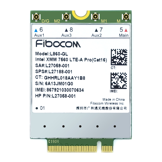
- Page 2 Applicability Type Product Model Description L860-GL-16 Reproduction forbidden without Fibocom Wireless Inc. written authorization - All Rights Reserved. FIBOCOM L860-GL Series Hardware Guide Page 2 of 60...
- Page 3 USI, or the host manufacturer can take responsibility through the change in FCC ID (new application) procedure followed by a Class II permissive change application. Reproduction forbidden without Fibocom Wireless Inc. written authorization - All Rights Reserved. FIBOCOM L860-GL Series Hardware Guide...
- Page 4 (including the transmitter) and obtaining a separate FCC/IC authorization. Manual Information to the End User Reproduction forbidden without Fibocom Wireless Inc. written authorization - All Rights Reserved. FIBOCOM L860-GL Series Hardware Guide Page 4 of 60...
- Page 5 Part 15 Subpart B compliance testing with the modular transmitter installed. This device is intended only for OEM integrators under the following conditions: (For Reproduction forbidden without Fibocom Wireless Inc. written authorization - All Rights Reserved. FIBOCOM L860-GL Series Hardware Guide Page 5 of 60...
- Page 6 This equipment complies with FCC radiation exposure limits set forth for an uncontrolled environment. This equipment should be installed and operated with minimum distance cm between the radiator & your body. Reproduction forbidden without Fibocom Wireless Inc. written authorization - All Rights Reserved. FIBOCOM L860-GL Series Hardware Guide Page 6 of 60...
- Page 7 Change History Version Author Date Remark V1.0.0 Shu Ying 2020-09-28 Draft version Reproduction forbidden without Fibocom Wireless Inc. written authorization - All Rights Reserved. FIBOCOM L860-GL Series Hardware Guide Page 7 of 60...
-
Page 8: Table Of Contents
USIM Interface......................37 USIM1 Pins ........................38 USIM Interface Circuit ....................38 3.5.2.1 N.C. SIM Card Slot ........................38 Reproduction forbidden without Fibocom Wireless Inc. written authorization - All Rights Reserved. FIBOCOM L860-GL Series Hardware Guide Page 8 of 60... - Page 9 M.2 Interface Model ....................56 M.2 Connector ......................57 Storage ........................58 Packing ........................58 Tray Package ........................ 58 Tray Size ........................60 Reproduction forbidden without Fibocom Wireless Inc. written authorization - All Rights Reserved. FIBOCOM L860-GL Series Hardware Guide Page 9 of 60...
-
Page 10: Foreword
PCI Express M.2 Specification Rev1.2 1.3 Related Documents FIBOCOM Design Guide_RF Antenna FIBOCOM L860 Series AT Commands_V3.4.1 Reproduction forbidden without Fibocom Wireless Inc. written authorization - All Rights Reserved. FIBOCOM L860-GL Series Hardware Guide Page 10 of 60... -
Page 11: Overview
Storage temperature: -40° C-+85° C Interface: M.2 Key-B Physical Dimension : 30×42×2.3mm Characteristics Weight: About 6.2 g Interface Antenna Connector WWAN Antenna×4 Reproduction forbidden without Fibocom Wireless Inc. written authorization - All Rights Reserved. FIBOCOM L860-GL Series Hardware Guide Page 11 of 60... - Page 12 When temperature goes beyond normal operating temperature range of -10°C-+55°C, RF performance of module may be slightly off 3GPP specifications. Reproduction forbidden without Fibocom Wireless Inc. written authorization - All Rights Reserved. FIBOCOM L860-GL Series Hardware Guide Page 12 of 60...
-
Page 13: Ca Combinations
2 inter-band 2+2+4+71,2+2+14+66,2+2+66+71,2+14+66+66,2+66+6 6+71, 2+5+5+30, 2+5+5+66, 2+5+46+46, 2+13+46+46, 2 intra-band (contiguous) plus 2+46+46+46, 2+46+46+66, 2+5+66+66, 2+13+66+66, 2 inter-band 2+66+66+71, Reproduction forbidden without Fibocom Wireless Inc. written authorization - All Rights Reserved. FIBOCOM L860-GL Series Hardware Guide Page 13 of 60... - Page 14 3 intra-band (contiguous) plus 2 46+46+46+66+66,5+5+46+46+46,7+7+46+46+46 intra-band (contiguous) 4 intra-band (contiguous) plus 2+46+46+46+46, 5+46+46+46+46, 13+46+46+46+46, inter-band 46+46+46+46+66 Intra-band (contiguous) 41,48 Intra-band (non-contiguous) Reproduction forbidden without Fibocom Wireless Inc. written authorization - All Rights Reserved. FIBOCOM L860-GL Series Hardware Guide Page 14 of 60...
-
Page 15: Application Framework
RF contains the followings: RF Transceiver RF Power/PA RF Front end RF Filter Antenna Connector Reproduction forbidden without Fibocom Wireless Inc. written authorization - All Rights Reserved. FIBOCOM L860-GL Series Hardware Guide Page 15 of 60... -
Page 16: Antenna Configuration
4×4 MIMO supported bands receive MIMO2 ANT 4×4 MIMO supported bands receive Diversity & GNSS ANT All supported bands and GNSS receive Reproduction forbidden without Fibocom Wireless Inc. written authorization - All Rights Reserved. FIBOCOM L860-GL Series Hardware Guide Page 16 of 60... -
Page 17: Application Interface
USB D+ FULL_CARD_POWER_OFF#(3.3/1.8V) +3.3V +3.3V CONFIG_3 Figure 3-1 Pin map Note: Pin “Notch” represents the gap of the gold fingers. Reproduction forbidden without Fibocom Wireless Inc. written authorization - All Rights Reserved. FIBOCOM L860-GL Series Hardware Guide Page 17 of 60... -
Page 18: Pin Definition
NC, L860 M.2 module is configured as the WWAN – PCIe, USB3.0 interface CONFIG_0 type UART_TX, MUX for UART_TX 1.8V ANT_TUNER_CONFIG/GPIO(High-z) Reproduction forbidden without Fibocom Wireless Inc. written authorization - All Rights Reserved. FIBOCOM L860-GL Series Hardware Guide Page 18 of 60... - Page 19 Master I2C1 DATA 1.8V PCIe TX differential signal PETp0 Positive I2C_IRQ# I2C1 INT, Wake up I2C HOST 1.8V Power Supply Reproduction forbidden without Fibocom Wireless Inc. written authorization - All Rights Reserved. FIBOCOM L860-GL Series Hardware Guide Page 19 of 60...
- Page 20 PCIe reference clock signal, Positive MIPI interface tunable ANT, RFFE_SCLK 1.8V RFFE clock Power Supply MIPI interface tunable ANT, RFFE_SDATA 1.8V RFFE data Reproduction forbidden without Fibocom Wireless Inc. written authorization - All Rights Reserved. FIBOCOM L860-GL Series Hardware Guide Page 20 of 60...
- Page 21 Voltage indication of PCIe side band. GND, Support PCIe Interface 3.3V. VIO_CFG NC, support 1.8V and compatible with 3.3V. +3.3V Power input Power Supply Reproduction forbidden without Fibocom Wireless Inc. written authorization - All Rights Reserved. FIBOCOM L860-GL Series Hardware Guide Page 21 of 60...
-
Page 22: Power
In addition, the DC/DC power supply other than PCIe ports should not be used as the external power cannot control the module status through the PCIe protocol. Reproduction forbidden without Fibocom Wireless Inc. written authorization - All Rights Reserved. FIBOCOM L860-GL Series Hardware Guide... -
Page 23: Power Supply
1500/1700/1800/1900, 18pF, 10pF, 2100/2300, 2500/2600MHz, Filter out medium/high frequency band RF 8.2pF, 6.8pF, 3500/3700MHz, 5GHz frequency interference 3.3pF band Reproduction forbidden without Fibocom Wireless Inc. written authorization - All Rights Reserved. FIBOCOM L860-GL Series Hardware Guide Page 23 of 60... -
Page 24: Logic Level
The L860 module 3.3V logic level definition is shown in the following table: Parameter Minimum Typical Maximum Unit 3.3V logic level 3.135 3.465 3.465 -0.3 Reproduction forbidden without Fibocom Wireless Inc. written authorization - All Rights Reserved. FIBOCOM L860-GL Series Hardware Guide Page 24 of 60... -
Page 25: Power Consumption
LTE FDD Data call Band 66 @+23dBm LTE FDD Data call Band 71 @+23dBm LTE TDD Data call Band 38 @+23dBm LTE TDD Reproduction forbidden without Fibocom Wireless Inc. written authorization - All Rights Reserved. FIBOCOM L860-GL Series Hardware Guide Page 25 of 60... -
Page 26: Control Signal
3.3/1.8V _OFF# Power on: High/Floating Power off: Low WWAN reset input, internal pull up RESET# 1.8V (10KΩ), active low Reproduction forbidden without Fibocom Wireless Inc. written authorization - All Rights Reserved. FIBOCOM L860-GL Series Hardware Guide Page 26 of 60... -
Page 27: Module Start-Up
FCPO# signal. After about 15s, module will complete initialization process. The start-up timing is shown in Figure 3-5: Reproduction forbidden without Fibocom Wireless Inc. written authorization - All Rights Reserved. FIBOCOM L860-GL Series Hardware Guide Page 27 of 60... -
Page 28: Module Shutdown
PMU. The control timing is shown in Figure 3-6: Reproduction forbidden without Fibocom Wireless Inc. written authorization - All Rights Reserved. FIBOCOM L860-GL Series Hardware Guide Page 28 of 60... -
Page 29: Module Reset
RESET# function, the PMU remains its power inside the module. The recommended circuit design is shown in the Figure 3-7: Reproduction forbidden without Fibocom Wireless Inc. written authorization - All Rights Reserved. FIBOCOM L860-GL Series Hardware Guide Page 29 of 60... - Page 30 +3.3V FCPO# RESET# off2 PERST# typical 15s Module State Activation Baseband reset Initialization Activation Figure 3-8 Reset control timing1 Reproduction forbidden without Fibocom Wireless Inc. written authorization - All Rights Reserved. FIBOCOM L860-GL Series Hardware Guide Page 30 of 60...
-
Page 31: Pcie Link State
D0 L1.2 Refer 3.2.3 Power Consumption sleep The extra 0.5mA is consumed on +0.5 cold sleep PERST# pull down Reproduction forbidden without Fibocom Wireless Inc. written authorization - All Rights Reserved. FIBOCOM L860-GL Series Hardware Guide Page 31 of 60... -
Page 32: D0 L1.2
L2 state in Win10 system. The D0->D3 L2@S0/S0ix cold cold ->D0 timing is shown in Figure 3-11 and Figure 3-12: Reproduction forbidden without Fibocom Wireless Inc. written authorization - All Rights Reserved. FIBOCOM L860-GL Series Hardware Guide Page 32 of 60... - Page 33 Modem assert Modem de-assert Module State D0 L0@S0/S0ix L2@S0/S0ix D0 L0@S0/S0ix cold Figure 3-12 D3 L2 timing (Modem wakeup) cold Reproduction forbidden without Fibocom Wireless Inc. written authorization - All Rights Reserved. FIBOCOM L860-GL Series Hardware Guide Page 33 of 60...
-
Page 34: Timing Application
MBIM port and a GNSS port in Win10 & Linux system. MBIM interface is used for initiating data service in Win10 & Linux system and GNSS interface is used for receiving GNSS data. Reproduction forbidden without Fibocom Wireless Inc. written authorization - All Rights Reserved. FIBOCOM L860-GL Series Hardware Guide... -
Page 35: Pcie Interface Definition
Active low, open drain output and should add external pull up (100KΩ) on platform Reproduction forbidden without Fibocom Wireless Inc. written authorization - All Rights Reserved. FIBOCOM L860-GL Series Hardware Guide Page 35 of 60... -
Page 36: Pcie Interface Application
When a serpentine line is used for length match with another line, the bended length of each segment should be at least 3 times the line width (≥ 3W). The largest spacing between the bended part of the Reproduction forbidden without Fibocom Wireless Inc. written authorization - All Rights Reserved. FIBOCOM L860-GL Series Hardware Guide... -
Page 37: Usim Interface
The L860 module support dual SIM card single standby, with one built-in USIM card interface, which supports 1.8V and 3V SIM cards. Reproduction forbidden without Fibocom Wireless Inc. written authorization - All Rights Reserved. FIBOCOM L860-GL Series Hardware Guide Page 37 of 60... -
Page 38: Usim1 Pins
When the SIM card is inserted, it connects an open circuit between CD and SW pins, and drives the SIM_DETECT pin high. Reproduction forbidden without Fibocom Wireless Inc. written authorization - All Rights Reserved. FIBOCOM L860-GL Series Hardware Guide Page 38 of 60... -
Page 39: Sim Card Slot
SIM_DETECT status will not be detected. After the SIM card hot-plug detection function is enabled, the module detects that the SIM card is inserted Reproduction forbidden without Fibocom Wireless Inc. written authorization - All Rights Reserved. FIBOCOM L860-GL Series Hardware Guide... -
Page 40: Usim Design
Module Status LED1# Signal RF function ON Low level (LED on) RF function OFF High level (LED off) Reproduction forbidden without Fibocom Wireless Inc. written authorization - All Rights Reserved. FIBOCOM L860-GL Series Hardware Guide Page 40 of 60... -
Page 41: Wowwan
Idle/Sleep Call/SMS/Data Figure 3-18 WOWWAN# timing Note: SMS wake-up host need send AT command: AT+GTSMSFILTERWUPEN=1 to enable this function. Reproduction forbidden without Fibocom Wireless Inc. written authorization - All Rights Reserved. FIBOCOM L860-GL Series Hardware Guide Page 41 of 60... -
Page 42: Interrupt Control
The module keeps the default emission power High/Floating Lower the maximum emission power to the threshold value of the module. Reproduction forbidden without Fibocom Wireless Inc. written authorization - All Rights Reserved. FIBOCOM L860-GL Series Hardware Guide Page 42 of 60... -
Page 43: Ant_Config
ANTCTL1 1.8V bit1 Tunable ANT control, GPO interface, ANTCTL2 1.8V Bit2 Tunable ANT control, GPO interface, ANTCTL3 1.8V Bit3 Reproduction forbidden without Fibocom Wireless Inc. written authorization - All Rights Reserved. FIBOCOM L860-GL Series Hardware Guide Page 43 of 60... -
Page 44: Configuration Interface
Master I2C1 DATA 1.8V I2C_IRQ# I2C1 INT, Wake up I2C HOST 1.8V Note: L860 works as a slave device. Reproduction forbidden without Fibocom Wireless Inc. written authorization - All Rights Reserved. FIBOCOM L860-GL Series Hardware Guide Page 44 of 60... -
Page 45: Radio Frequency
L860 module uses standard M.2 RF connectors. The RF connector part number is 818004607 manufactured by ECT corporation, and the size is 2×2×0.6mm. The connector dimension is shown as Reproduction forbidden without Fibocom Wireless Inc. written authorization - All Rights Reserved. FIBOCOM L860-GL Series Hardware Guide... - Page 46 Figure 4-3 0.81mm coaxial antenna dimensions Figure 4-4 Schematic diagram of 0.81mm coaxial antenna connected to the RF connector Reproduction forbidden without Fibocom Wireless Inc. written authorization - All Rights Reserved. FIBOCOM L860-GL Series Hardware Guide Page 46 of 60...
-
Page 47: Rf Connector Assembly
JIG must be lifted up vertically to PCB surface (see Figure 4-7 and 4-8). Figure 4-6 Pulling JIG Figure 4-7 Lift up pulling JIG Reproduction forbidden without Fibocom Wireless Inc. written authorization - All Rights Reserved. FIBOCOM L860-GL Series Hardware Guide Page 47 of 60... -
Page 48: Operating Band
Band 26 850MHz LTE FDD 814-849 859-894 Band 29 700MHz LTE FDD 716-728 Band 30 2300MHz LTE FDD 2305-2315 2350-2360 Reproduction forbidden without Fibocom Wireless Inc. written authorization - All Rights Reserved. FIBOCOM L860-GL Series Hardware Guide Page 48 of 60... -
Page 49: Transmitting Power
Band 26 23± 2.7 23+2/-1 10MHz Bandwidth, 1 RB Band 30 23± 2.7 22± 1 10MHz Bandwidth, 1 RB Reproduction forbidden without Fibocom Wireless Inc. written authorization - All Rights Reserved. FIBOCOM L860-GL Series Hardware Guide Page 49 of 60... -
Page 50: Receiver Sensitivity
10MHz Bandwidth Band 26 -93.8 -103.0 10MHz Bandwidth Band 29 -93.3 -101 10MHz Bandwidth Band 30 -95.3 -101 10MHz Bandwidth Reproduction forbidden without Fibocom Wireless Inc. written authorization - All Rights Reserved. FIBOCOM L860-GL Series Hardware Guide Page 50 of 60... -
Page 51: Four Antennas Receiver Sensitivity
The above values are measured in four antennas condition (Main+Diversity+M1+M2). If only use dual antennas (Main+Diversity), the sensitivity will drop about 3dBm for each band of LTE. Reproduction forbidden without Fibocom Wireless Inc. written authorization - All Rights Reserved. FIBOCOM L860-GL Series Hardware Guide... -
Page 52: Gnss
The L860 module provides main and diversity antenna interfaces, and the antenna design requirements are shown in the following table: Reproduction forbidden without Fibocom Wireless Inc. written authorization - All Rights Reserved. FIBOCOM L860-GL Series Hardware Guide Page 52 of 60... - Page 53 ANT on B30 suggestion: Peak gain < 1dBi, for FCC EIRP requirement, Efficient > 50% for carrier TRP requirement. If integrator doesn't follow the instruction, may cause FCC EIRP or carrier TRP certification fail. Reproduction forbidden without Fibocom Wireless Inc. written authorization - All Rights Reserved. FIBOCOM L860-GL Series Hardware Guide Page 53 of 60...
-
Page 54: Esd Characteristics
±15 kV Antenna Interface ±8 kV Golden Finger ±2 kV Note: ESD performance is based on EVB-M2 development board. Reproduction forbidden without Fibocom Wireless Inc. written authorization - All Rights Reserved. FIBOCOM L860-GL Series Hardware Guide Page 54 of 60... -
Page 55: Structure Specification
The label of each module is subject to the good shipped. 6.2 Dimension of Structure The structural dimension of the L860 module is shown in Figure 6-2: Reproduction forbidden without Fibocom Wireless Inc. written authorization - All Rights Reserved. FIBOCOM L860-GL Series Hardware Guide Page 55 of 60... -
Page 56: Interface Model
Structure. Based on the M.2 interface definition, L860 module adopts Type 3042-S3-B interface (30x42mm, the component maximum height on t top layer is 1.5mm, PCB thickness is 0.8mm, and KEY ID is B). Reproduction forbidden without Fibocom Wireless Inc. written authorization - All Rights Reserved. FIBOCOM L860-GL Series Hardware Guide... -
Page 57: Connector
APCI0026-P001A manufactured by LOTES Corporation, and the dimension is shown in Figure 6-4. The package of connector, please refer to the specification. Figure 6-4 M.2 dimension of structure Reproduction forbidden without Fibocom Wireless Inc. written authorization - All Rights Reserved. FIBOCOM L860-GL Series Hardware Guide Page 57 of 60... -
Page 58: Storage
The L860 module uses tray package, 20 pcs are packed in each tray, with 5 trays including one empty tray on top in each box and 5 boxes in each case. Tray packaging process is shown in Figure 6-5: Reproduction forbidden without Fibocom Wireless Inc. written authorization - All Rights Reserved. FIBOCOM L860-GL Series Hardware Guide... - Page 59 Figure 6-5 Tray packaging process Reproduction forbidden without Fibocom Wireless Inc. written authorization - All Rights Reserved. FIBOCOM L860-GL Series Hardware Guide Page 59 of 60...
-
Page 60: Tray Size
Figure 6-6 Tray size (unit: mm) ITEM DIM (Unit: mm) 315.0±2.0 170.0±2.0 6.5±0.3 0.8±0.1 43.0±0.3 31.0±0.3 79.0±0.2 60.0±0.2 180.0±0.2 60.0±0.2 40.0±0.2 Reproduction forbidden without Fibocom Wireless Inc. written authorization - All Rights Reserved. FIBOCOM L860-GL Series Hardware Guide Page 60 of 60...
Need help?
Do you have a question about the L860-GL-16 and is the answer not in the manual?
Questions and answers