Table of Contents
Advertisement
Advertisement
Table of Contents

Related Manuals for Fibocom FM350-GL


Summary of Contents for Fibocom FM350-GL
- Page 1 FM350-GL Hardware Guide General Version: V1.0.6 Date: 2020-04-25...
- Page 2 Applicability Type Product model Description FM350-GL-00 Reproduction forbidden without Fibocom Wireless Inc. written authorization - All Rights Reserved. FM350-GL Hardware Guide Page 2 of 67...
- Page 3 Trademark The trademark is registered and owned by Fibocom Wireless Inc. Reproduction forbidden without Fibocom Wireless Inc. written authorization - All Rights Reserved. FM350-GL Hardware Guide Page 3 of 67...
- Page 4 2020-6-30 ● Update FCPO# and RESET# recommended design ● Update WWAN M.2 module type configuration V1.0.0 Lei Daijun 2020-4-30 Draft version Reproduction forbidden without Fibocom Wireless Inc. written authorization - All Rights Reserved. FM350-GL Hardware Guide Page 4 of 67...
-
Page 5: Table Of Contents
D0 L1.2 ............................31 3.3.4.2 L2............................. 32 cold Timing Application ....................... 33 PCIe Interface ......................33 PCIe Interface Definition ..................... 33 Reproduction forbidden without Fibocom Wireless Inc. written authorization - All Rights Reserved. FM350-GL Hardware Guide Page 5 of 67... - Page 6 Antenna Design ......................56 ESD Characteristics ....................58 Structure Specification ....................59 Product Appearance ..................... 59 Dimension of Structure ....................59 M.2 Interface Model...................... 60 Reproduction forbidden without Fibocom Wireless Inc. written authorization - All Rights Reserved. FM350-GL Hardware Guide Page 6 of 67...
- Page 7 Top-mount Connection with Single-Sided Module ............64 Storage ......................... 65 Storage Life ........................ 65 Packing ........................65 Tray Package ......................65 Tray Size ........................67 Reproduction forbidden without Fibocom Wireless Inc. written authorization - All Rights Reserved. FM350-GL Hardware Guide Page 7 of 67...
-
Page 8: Foreword
The document describes the electrical characteristics, RF performance, dimensions and application environment, etc. of FM350-GL (hereinafter referred to as FM350). With the assistance of the document and other instructions, the developers can quickly understand the hardware functions of FM350 modules and develop products. -
Page 9: Related Document
1.3 Related Document FIBOCOM Design Guide_RF Antenna Reproduction forbidden without Fibocom Wireless Inc. written authorization - All Rights Reserved. FM350-GL Hardware Guide Page 9 of 67... -
Page 10: Overview
3GPP Release 15 100MHz 5 DLCA, 256 QAM LTE Modulation 40MHz 2 ULCA, 256 QAM 3GPP Release 8 UMTS Modulation RF Characteristic Reproduction forbidden without Fibocom Wireless Inc. written authorization - All Rights Reserved. FM350-GL Hardware Guide Page 10 of 67... -
Page 11: Key Features
Characteristics Weight: 8g Interface WWAN Antenna x 4 Antenna Connector Support 4x4 MIMO Function Interface Dual SIM (one built-in eSIM), 1.8V/3V Reproduction forbidden without Fibocom Wireless Inc. written authorization - All Rights Reserved. FM350-GL Hardware Guide Page 11 of 67... -
Page 12: Ca Combinations
3) When temperature goes beyond normal operating temperature range of -10°C to +55°C, RF performance of module may be slightly off 3GPP specifications. 2.3 CA Combinations DL CA Combinations Inter-band Intra-band Reproduction forbidden without Fibocom Wireless Inc. written authorization - All Rights Reserved. FM350-GL Hardware Guide Page 12 of 67... - Page 13 DL CA Combinations Inter-band Intra-band Inter-band Intra-band Inter-band Intra-band Reproduction forbidden without Fibocom Wireless Inc. written authorization - All Rights Reserved. FM350-GL Hardware Guide Page 13 of 67...
-
Page 14: Application Block
● RF ET Power/PA ● MCP (NAND+LPDDR4 RAM) ● RF PAMid/Front end ● Application interface ● RF SW ● RF Multi-plexer/Filter Reproduction forbidden without Fibocom Wireless Inc. written authorization - All Rights Reserved. FM350-GL Hardware Guide Page 14 of 67... -
Page 15: Antenna Configuration
Transmit, 4x4 MIMO receive ANT2(M2) 1452~5000 and SRS Diversity & GNSS ANT All supported bands and ANT3(D/G) 617~5925 and SRS GNSS receive, SRS Reproduction forbidden without Fibocom Wireless Inc. written authorization - All Rights Reserved. FM350-GL Hardware Guide Page 15 of 67... -
Page 16: Application Interface
The FM350 module applies standard M.2 Key-B interface, with a total of 75 pins. Pin Map Figure 3-1 Pin Map Note: Pin “Notch” represents the gap of the gold fingers. Reproduction forbidden without Fibocom Wireless Inc. written authorization - All Rights Reserved. FM350-GL Hardware Guide Page 16 of 67... -
Page 17: Pin Definition
WWAN – PCIe Gen3, USB3.1 21 CONFIG_0 Gen1 interface type UART TXD output , can mux as 22 UART_TX ANT_TUNER_CFG or GPIO. 1.8V Reserved Reproduction forbidden without Fibocom Wireless Inc. written authorization - All Rights Reserved. FM350-GL Hardware Guide Page 17 of 67... - Page 18 PCIe TX differential signals positive I2C interrupt request 1.8V 44 I2C_IRQ# 45 GND Power Supply 46 NC PCIe RX differential signals 47 PERn0 negative Reproduction forbidden without Fibocom Wireless Inc. written authorization - All Rights Reserved. FM350-GL Hardware Guide Page 18 of 67...
- Page 19 Tunable ANT CTRL0 1.8V Wireless coexistence between WWAN and WiFi/BT modules, based on BT-SIG 60 COEX3 1.8V coexistence protocol. COEX_EXT_FTA, Reserved Reproduction forbidden without Fibocom Wireless Inc. written authorization - All Rights Reserved. FM350-GL Hardware Guide Page 19 of 67...
- Page 20 Power input Power Supply GND, FM350 M.2 module is configured as the WWAN – PCIe Gen3, USB3.1 75 CONFIG_2 Gen1 interface type Reproduction forbidden without Fibocom Wireless Inc. written authorization - All Rights Reserved. FM350-GL Hardware Guide Page 20 of 67...
-
Page 21: Power Supply
In addition, the DC/DC power supply other than PCIe ports should not be used as the external power cannot control the module status through the PCIe protocol. Reproduction forbidden without Fibocom Wireless Inc. written authorization - All Rights Reserved. FM350-GL Hardware Guide... -
Page 22: Power Supply
300mV in design. Module supports 5G NR Sub-6 download, when module operates with the maximum data transfer throughput, the peak current can reach to upper 3500mA. It Reproduction forbidden without Fibocom Wireless Inc. written authorization - All Rights Reserved. FM350-GL Hardware Guide... -
Page 23: Logic Level
In the condition of 3.3V power supply, the FM350 power consumption is shown in the following table: Average Parameter Mode Condition Current (mA) Power supply, module power off Power off WCDMA DRX=8 Sleep Reproduction forbidden without Fibocom Wireless Inc. written authorization - All Rights Reserved. FM350-GL Hardware Guide Page 23 of 67... - Page 24 Band5 Band8 Band1 Band2 Band3 Band4 Band5 Band7 Band8 Band12 LTE FDD LTE-RMS Band13 Band14 Band17 Band18 Band19 Band20 Band25 Band26 Reproduction forbidden without Fibocom Wireless Inc. written authorization - All Rights Reserved. FM350-GL Hardware Guide Page 24 of 67...
- Page 25 Average Parameter Mode Condition Current (mA) Band28 Band30 Band66 Band71 Band34 Band38 Band39 Band40 LTE TDD Band41 Band42 Band43 Band48 NR-RMS Reproduction forbidden without Fibocom Wireless Inc. written authorization - All Rights Reserved. FM350-GL Hardware Guide Page 25 of 67...
-
Page 26: Control Signal
If module went into PERST# core dump, it will reset whole 3.3/1.8V module, not only PCIe interface. Active low, internal pull up(10KΩ) Reproduction forbidden without Fibocom Wireless Inc. written authorization - All Rights Reserved. FM350-GL Hardware Guide Page 26 of 67... -
Page 27: Module Start-Up
When power supply is ready, the PMU of module will power on and start initialization process by pulling high FCPO# signal. After about 20s, module will complete initialization process. The start-up timing is shown in Figure 3-5: Reproduction forbidden without Fibocom Wireless Inc. written authorization - All Rights Reserved. FM350-GL Hardware Guide Page 27 of 67... -
Page 28: Module Shutdown
PMU. The control timing is shown in Figure 3-6: Reproduction forbidden without Fibocom Wireless Inc. written authorization - All Rights Reserved. FM350-GL Hardware Guide Page 28 of 67... -
Page 29: Module Reset
RESET# function, the PMU remains its power inside the module. The recommended circuit design is shown in the Figure 3-7: Figure 3-7 Recommended design for reset circuit Reproduction forbidden without Fibocom Wireless Inc. written authorization - All Rights Reserved. FM350-GL Hardware Guide Page 29 of 67... - Page 30 500ms 500ms again. This is required for both Pre-OS as well as Runtime flow Reproduction forbidden without Fibocom Wireless Inc. written authorization - All Rights Reserved. FM350-GL Hardware Guide Page 30 of 67...
-
Page 31: Pcie Link State
D0 L1.2@S0/S0ix→D0 L0@S0/S0ix timing is shown in figure 3-10: +3.3V FCPO# RESET# PERST# CLKREQ# Module State D0 L0@S0/S0ix D0 L1.2@S0/S0ix D0 L0@S0/S0ix Figure 3-10 D0 L1.2 timing Reproduction forbidden without Fibocom Wireless Inc. written authorization - All Rights Reserved. FM350-GL Hardware Guide Page 31 of 67... -
Page 32: D3 Cold L2
PEWAKE# Modem assert Modem de-assert Module State D0 L0@S0/S0ix L2@S0/S0ix D0 L0@S0/S0ix cold Figure 3-12 D3 L2 timing (modem wakeup) cold Reproduction forbidden without Fibocom Wireless Inc. written authorization - All Rights Reserved. FM350-GL Hardware Guide Page 32 of 67... -
Page 33: Timing Application
PCIe TX Differential signals, positive PETP0 PERn0 PCIe RX Differential signals, negative PERP0 PCIe RX Differential signals, positive PCIe Reference Clock signal REFCLKN Negative Reproduction forbidden without Fibocom Wireless Inc. written authorization - All Rights Reserved. FM350-GL Hardware Guide Page 33 of 67... -
Page 34: Pcie Interface Application
RXP/N and clock pair CLKP/N. PCIe can achieve the maximum transmission rate of 8 GT/s, and must strictly follow the rules below in PCB Layout: Reproduction forbidden without Fibocom Wireless Inc. written authorization - All Rights Reserved. FM350-GL Hardware Guide Page 34 of 67... - Page 35 Reproduction forbidden without Fibocom Wireless Inc. written authorization - All Rights Reserved. FM350-GL Hardware Guide...
-
Page 36: Usim Interface
3.5.2.1 N.C. SIM Card Slot The reference circuit design for N.C. (Normally Closed) SIM card slot is shown in Figure 3-16: Reproduction forbidden without Fibocom Wireless Inc. written authorization - All Rights Reserved. FM350-GL Hardware Guide Page 36 of 67... -
Page 37: Sim Card Slot
When the SIM card is inserted, it connects the short circuit between CD and SW pins, and drives the SIM_DETECT pin high. Reproduction forbidden without Fibocom Wireless Inc. written authorization - All Rights Reserved. FM350-GL Hardware Guide Page 37 of 67... -
Page 38: Usim Hot-Plug
The filter capacitors and ESD devices for SIM card signals should be placed near to the SIM card slot, and the ESD devices with 22 to 33pF capacitance should be used. Reproduction forbidden without Fibocom Wireless Inc. written authorization - All Rights Reserved. FM350-GL Hardware Guide... -
Page 39: Status Indicator
Figure 3-18 LED driving circuit Note: The resistance of LED current-limiting resistor is selected according to the driving voltage and the driving current. Reproduction forbidden without Fibocom Wireless Inc. written authorization - All Rights Reserved. FM350-GL Hardware Guide Page 39 of 67... -
Page 40: Wowwan
Enable/Disable RF network W_DISABLE1# 3.3/1.8V Dynamic Power Reduction - Body SAR control signal 3.3/1.8V (SAR_BACK_OFF) GNSS Disable signal W_DISABLE2# 3.3/1.8V Reserved Reproduction forbidden without Fibocom Wireless Inc. written authorization - All Rights Reserved. FM350-GL Hardware Guide Page 40 of 67... -
Page 41: W_Disable1
GPIO. 1.8V Reserved Tunable ANT control, MIPI Interface, RFFE_SCLK 1.8V RFFE clock Tunable ANT control, MIPI Interface, RFFE_SDATA 1.8V RFFE data Reproduction forbidden without Fibocom Wireless Inc. written authorization - All Rights Reserved. FM350-GL Hardware Guide Page 41 of 67... -
Page 42: Configuration Interface
(pin1) Main Host Interface WWAN–PCIe Gen3, USB3.1 Vendor defined Gen1 Please refer to “PCI Express M.2 Specification Rev1.2” for more details. Reproduction forbidden without Fibocom Wireless Inc. written authorization - All Rights Reserved. FM350-GL Hardware Guide Page 42 of 67... -
Page 43: Radio Frequency
Figure 4-1 RF connectors RF Connector Characteristic Rated Condition Environment Condition Frequency Range DC~6GHz Temperature Range: –40° C to +85° C 50Ω Characteristic Impedance Reproduction forbidden without Fibocom Wireless Inc. written authorization - All Rights Reserved. FM350-GL Hardware Guide Page 43 of 67... -
Page 44: Rf Connector Dimension
ECT Corporation, and the connector size is 2x2x0.6m. The connector dimension is shown as following picture: Figure 4-2 RF connector dimensions Figure 4-3 0.81mm coaxial antenna dimensions Reproduction forbidden without Fibocom Wireless Inc. written authorization - All Rights Reserved. FM350-GL Hardware Guide Page 44 of 67... -
Page 45: Rf Connector Assembly
To avoid damage in RF connector unmating, it is recommended using pulling JIG as Figure 4-6, and the pulling JIG must be lifted up vertically to PCB surface (see Figure 4-7 and 4-8). Figure 4-6 Pulling JIG Reproduction forbidden without Fibocom Wireless Inc. written authorization - All Rights Reserved. FM350-GL Hardware Guide Page 45 of 67... - Page 46 Figure 4-7 Lift up pulling JIG Figure 4-8 Pulling direction Reproduction forbidden without Fibocom Wireless Inc. written authorization - All Rights Reserved. FM350-GL Hardware Guide Page 46 of 67...
-
Page 47: Operating Band
LTE TDD 2300 - 2400 2496 - 2690 Band 41 2500MHz LTE TDD 3400 - 3600 Band 42 3500MHZ LTE TDD Reproduction forbidden without Fibocom Wireless Inc. written authorization - All Rights Reserved. FM350-GL Hardware Guide Page 47 of 67... - Page 48 NR TDD 4400 - 5000 NR TDD GPS L1 1575.42± 1.023 GLONASS G1 1602.5625±4 Galileo E1 1575.42± 2.046 BDS B1 1561.098± 2.046 Reproduction forbidden without Fibocom Wireless Inc. written authorization - All Rights Reserved. FM350-GL Hardware Guide Page 48 of 67...
-
Page 49: Transmitting Power
10MHz Bandwidth, 1 RB Band 38 23± 2.7 23± 1 10MHz Bandwidth, 1 RB Band 39 23± 2.7 23± 1 10MHz Bandwidth, 1 RB Reproduction forbidden without Fibocom Wireless Inc. written authorization - All Rights Reserved. FM350-GL Hardware Guide Page 49 of 67... - Page 50 26+3/-4 25± 1 50MHz BW, Inner RB 26+3/-4 26± 1 50MHz BW, Inner RB 26+3/-4 26± 1 60MHz BW, Inner RB Reproduction forbidden without Fibocom Wireless Inc. written authorization - All Rights Reserved. FM350-GL Hardware Guide Page 50 of 67...
-
Page 51: Receiver Sensitivity
10MHz Bandwidth Band 26 -93.8 10MHz Bandwidth Band 28 -94.8 10MHz Bandwidth Band 29 -93.3 10MHz Bandwidth Band 30 -95.3 10MHz Bandwidth Reproduction forbidden without Fibocom Wireless Inc. written authorization - All Rights Reserved. FM350-GL Hardware Guide Page 51 of 67... - Page 52 SCS 30KHz 30MHz BW -86.2 SCS 30KHz 60MHz BW -91.9 SCS 30KHz 20MHz BW -92.6 SCS 15KHz 20MHz BW -90.9 SCS 15KHz 10MHz BW Reproduction forbidden without Fibocom Wireless Inc. written authorization - All Rights Reserved. FM350-GL Hardware Guide Page 52 of 67...
-
Page 53: Four Antenna Receiver Sensitivity
10MHz Bandwidth LTE TDD Band 40 10MHz Bandwidth Band 41 10MHz Bandwidth Band 42 -97.2 10MHz Bandwidth Band 43 -97.2 10MHz Bandwidth Reproduction forbidden without Fibocom Wireless Inc. written authorization - All Rights Reserved. FM350-GL Hardware Guide Page 53 of 67... - Page 54 The above values are measured in four antennas condition (Main+Diversity+M1+M2). If only use dual antennas (Main+Diversity), the sensitivity will drop about 3dBm for each band. Reproduction forbidden without Fibocom Wireless Inc. written authorization - All Rights Reserved. FM350-GL Hardware Guide...
-
Page 55: Gnss
Cold start TTFF Warm start Hot Start Tracking Sensitivity Acquisition Note: GNSS current is tested with RF disabled at 25℃ temperature. Reproduction forbidden without Fibocom Wireless Inc. written authorization - All Rights Reserved. FM350-GL Hardware Guide Page 55 of 67... -
Page 56: Antenna Design
LTE band 48 (3600): 150MHz LTE band 66 (1700): 490MHz LTE band 71 (600): 81MHz n1 (2100): 250MHz n2 (1900): 140MHz n3 (1800): 170MHz Reproduction forbidden without Fibocom Wireless Inc. written authorization - All Rights Reserved. FM350-GL Hardware Guide Page 56 of 67... - Page 57 BDS: 4MHz QZSS: Impedance 50Ω Input power > 28dBm average power WCDMA & LTE & NR Recommended standing-wave ≤ 2:1 ratio (SWR) Reproduction forbidden without Fibocom Wireless Inc. written authorization - All Rights Reserved. FM350-GL Hardware Guide Page 57 of 67...
-
Page 58: Esd Characteristics
±8 kV ±15 kV Antenna Interface ±8 kV Golden Finger ±2 kV Note: ESD performance is based on EVB-M2 development board. Reproduction forbidden without Fibocom Wireless Inc. written authorization - All Rights Reserved. FM350-GL Hardware Guide Page 58 of 67... -
Page 59: Structure Specification
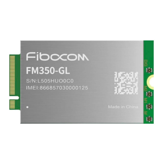
The product appearance for FM350 module is shown in Figure 6-1: Figure 6-1 Module appearance 6.2 Dimension of Structure The structural dimension of the FM350 module is shown in Figure 6-2: Reproduction forbidden without Fibocom Wireless Inc. written authorization - All Rights Reserved. FM350-GL Hardware Guide Page 59 of 67... -
Page 60: Interface Model
(30x52mm, the component maximum height on t top layer is 1.5mm, PCB thickness is 0.8mm, and KEY ID is B). Reproduction forbidden without Fibocom Wireless Inc. written authorization - All Rights Reserved. FM350-GL Hardware Guide Page 60 of 67... -
Page 61: Connector
LOTES Corporation, and the dimension is shown in Figure 6-5. The package of connector, please refer to the specification. Reproduction forbidden without Fibocom Wireless Inc. written authorization - All Rights Reserved. FM350-GL Hardware Guide Page 61 of 67... - Page 62 Figure 6-4 M.2 Dimension of structure for stack-up Mid-mount single-sided module Figure 6-5 M.2 dimension of structure for stack-up top-mount single-sided module Reproduction forbidden without Fibocom Wireless Inc. written authorization - All Rights Reserved. FM350-GL Hardware Guide Page 62 of 67...
-
Page 63: Card Assembly
APCI0026-P001A, the maximum angle of insertion is 20°. PLS refer to Figure 6-6 and Figure 6-7 to insert and extract the module. Figure 6-6 Angle of insertion for APCI0144-P001A Figure 6-7 Angle of insertion for APCI0026-P001A Reproduction forbidden without Fibocom Wireless Inc. written authorization - All Rights Reserved. FM350-GL Hardware Guide Page 63 of 67... -
Page 64: Mid-Mount Connection With Single-Sided Module
Full keep out area 30×42mm below module, which means don’t place any components and routings below M.2 module Add thermal pad between M.2 module and mother board for thermal dissipation. Reproduction forbidden without Fibocom Wireless Inc. written authorization - All Rights Reserved. FM350-GL Hardware Guide Page 64 of 67... -
Page 65: Storage
The FM350 module uses tray package, 20 pcs are packed in each tray, with 5 trays including one empty tray on top in each box and 5 boxes in each case. Tray packaging process is shown in Figure 6-10: Reproduction forbidden without Fibocom Wireless Inc. written authorization - All Rights Reserved. FM350-GL Hardware Guide... - Page 66 Figure 6-10 Tray packaging process Reproduction forbidden without Fibocom Wireless Inc. written authorization - All Rights Reserved. FM350-GL Hardware Guide Page 66 of 67...
-
Page 67: Tray Size
Tray Size The pallet size is 330x175x6.5mm, and is shown in Figure 6-11: Figure 6-11 Tray size (unit: mm) Reproduction forbidden without Fibocom Wireless Inc. written authorization - All Rights Reserved. FM350-GL Hardware Guide Page 67 of 67...
Need help?
Do you have a question about the FM350-GL and is the answer not in the manual?
Questions and answers