Advertisement
Quick Links
Advertisement

Related Manuals for NAD T748


Summary of Contents for NAD T748
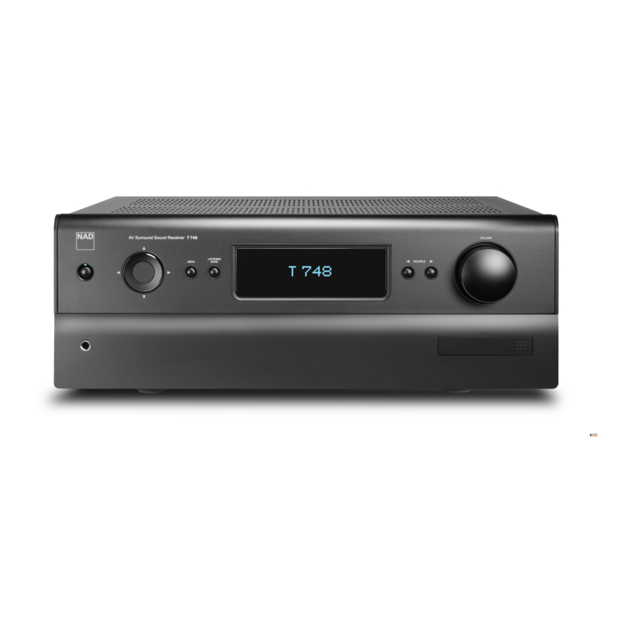
- Page 1 T748 AV Surround Sound Receiver...
-
Page 2: Table Of Contents
SECTION 1 SUMMARY CONTENTS PRODUCT SAFETY SERVICING GUIDELINES ..................SERVICING PRECAUTIONS ........................* General Servicing Precautions * Insulation checking prodedure * Electrostatically Sensitive Devices SPECIFICATIONS ........................................................DISASSEMBLY PRINCIPAL PART LOCATION ........................EXPLODED VIE ............................ -
Page 3: Product Safety Servicing Guidelines
PRODUCT SAFETY SERVICING GUIDELINES CAUTION : DO NOT ATTEMPT TO MODIFY THIS PRODUCT IN VOLTAGE MEASURE MUST NOT EXCEED 75 VOLTS R.M.S. ANY WAY. NEVER PERFORM CUSTOMIZED INSTALLATIONS THIS CORRESPONDS TO 0.5 MILLIAMP AC ANY VALUE WITHOUT MANUFACTURER’S APPROVAL. UNAUTHORIZED EXCEEDING THIS LIMIT CONSTITUTES A POTENTIAL MODIFICATIONS WILL NOT ONLY VOID THE WARRANTY, BUT SHOCK HAZARD AND MUST BE CORRECTED IMMEDIATELY. -
Page 4: Servicing Precautions
SERVICING PRECAUTIONS CAUTION : Before servicing the A/V Receiver covered by this Electrostatically Sensitive (ES) Devices service data and its supplements and addends, read and follow the Some semiconductor (solid state) devices can be damaged easily by SAFETY PRECAUTIONS. NOTE : if unforeseen circumstances static electricity. -
Page 5: Specifications
SPECIFICATIONS Amplifier Section FM Tuner Section (Without notes 100.1MHz, 60dB) Output Power(Front): i n i 20Hz to 20KHz with no more than 0.08% AH : 45 dB Surround Output Power (0.08% THD, 1KHz, 8 ohms): ) r r 45 + 45 Watt (Back Surr) Freqency Response : 50Hz - 13KHz, +3/-3dB Total Harmonic Distortion (Front): Audio input Sensitivity/Impedance :... -
Page 6: Disassembly
DISASSEMBLY REMOVAL OF FRONT PANEL... -
Page 7: Principal Part Location
PRINCIPAL PART LOCATION... - Page 8 T748AH EXPLODED VIEW PARTS LIST DESCRIPTION PARTS NO Q,ty REMARK DESCRIPTION PARTS NO. Q,ty WINDOW ,FIP CGU1A434Z SCREW CTB3+8JFZR VOLUME KNOB ASS'Y CGK1A145ZA KNOB,VOLUME CBN1A216 CAP,VOLUME CGK1A145C64 PANEL,AL CKM1A208XC64 SCREW CTWS3+10GR PANEL,FRONT CGW2A475RBB29 SCREW CTB4+6FFZR COVER,JACK CGR1A476B29 SCREW CTW3+12JR BRACKET CMD2A563 SCREW,SPECIAL CHD1A012R...
- Page 9 T748AH EXPLODED VIEW 31-2 31-3 29-1 31-4 31-1 28-2 27-2 29-2 27-5 27-7 28-1 27-1 27-8 27-6 27-4 27-3 1-10...
- Page 10 T748C EXPLODED VIEW PARTS LIST DESCRIPTION PARTS NO Q,ty REMARK Q,ty DESCRIPTION PARTS NO. WINDOW ,FIP CGU1A434Z SCREW CTB3+8JFZR VOLUME KNOB ASS'Y CGK1A145ZA SCREW CTB3+8JFC KNOB,VOLUME CBN1A216 SCREW CTWS3+10GR CAP,VOLUME CGK1A145C64 CKM1A208XC64 SCREW CTB4+6FFZR PANEL,AL PANEL,FRONT CGW2A475RBB29 SCREW CTW3+12JR COVER,JACK CGR1A476B29 SCREW,SPECIAL CHD1A012R...
- Page 11 T748C EXPLODED VIEW 31-2 29-2 31-3 29-1 31-4 31-1 28-2 27-2 27-5 27-7 28-1 27-1 27-8 27-6 27-4 27-3 1-12 1-13...
- Page 12 T748CT EXPLODED VIEW PARTS LIST DESCRIPTION PARTS NO Q,ty REMARK DESCRIPTION PARTS NO. Q,ty WINDOW ,FIP CGU1A434Z SCREW CTB3+8JFZR VOLUME KNOB ASS'Y CGK1A145YA SCREW CTB3+8JFC KNOB,VOLUME CBN1A216 SCREW CTWS3+10GR CAP,VOLUME CGK1A145C37 PANEL,AL CKM1A208XC37 SCREW CTB4+6FC PANEL,FRONT CGW2A475RBG38 SCREW CTW3+12JR COVER,JACK CGR1A476G38 SCREW,SPECIAL CHD1A012R...
- Page 13 T748CT EXPLODED VIEW 31-2 29-2 31-3 29-1 31-4 31-1 28-2 27-2 27-5 27-7 28-1 27-1 27-8 27-6 27-4 27-3 1-15 1-16...
- Page 14 IC BLOCK DIAGRAMS & PIN DESCRIPTION IC101 : STM32F103ZET6 (FLASH MCU) IC BLOCK DIAGRAMS TRACECLK TRACED[0:3] @V DD TPIU as AS Trace/trig Trace Power Pbus V DD SW/JTAG controller NJTRST Volt. reg. V SS JTDI 3.3 V to 1.8 V Ibus JTCK/SWCLK Flash 512 Kbytes...
- Page 15 IC PIN DESCRIPTION DD_2 SS_2 PA13 PA12 VBAT PA11 PC13-TAMPER-RTC PA10 PC14-OSC32_IN PC15-OSC32_OUT DD_9 SS_9 SS_5 LQFP144 DD_5 PF10 OSC_IN PD15 OSC_OUT PD14 NRST DD_8 SS_8 PD13 PD12 PD11 PD10 REF- REF+ PB15 PA0-WKUP PB14 PB13 PB12 ai14667...
- Page 16 IC 301 : R2A15218FP (INPUT SELECTOR TONE CONTROL) BLOCK DIAGRAM AND PIN CONFIGURATION (TOP VIEW) AVCC MUTE AVCC N.C. AVEE AVEE N.C. TREL 0/-6/-12/-18dB ADCL BASSL2 BASSL1 ADCR N.C. AGND Bass/ Treble 0~-95dB, -14~+14dB -∞ +42~0dB MAIN N.C. (2dB step) (0.5dBstep) (0.5dBstep) Bypass...
- Page 17 PIN DESCRIPTION PIN No. Function Name 23,21, FROUT,FLOUT, 17,15, COUT,SWOUT, Output pin of FL/FR/C/SW/SL/SR/SBL/SBR channel 11,9, SROUT, SLOUT, SBROUT,SBLOUT 24,20, FRC,FLC, 18,14, CC,SWC, Connects capacitor for reducing click noise of 12,8, SRC,SLC, L/R/C/SW/SL/SR/SBL/SBR channel volume SBRC,SBLC 4,7,10,16, Analog ground of internal circuit AGND 19,22,56 TREL, TRER...
- Page 18 IC 211 : MX29LV32DTTI - 70G (FLASH OF DSP)
- Page 20 IC 201 : TMS320DA788B (AUDIO DSP) Device Block Diagram Program/Data JTAG EMU 256K Bytes McASP0 Data 16 Serializers Program/Data C67x+ CPU ROM Page1 256K Bytes Memory Data Controller Program/Data McASP1 ROM Page2 6 Serializers 256K Bytes Program Fetch Program/Data McASP2 ROM Page3 2 Serializers 256K Bytes...
- Page 21 Pin Maps SPI0_SIMO EM_CKE SPI0_SOMI/I2C0_SDA EM_CLK AXR0[0] EM_WE_DQM[1] AXR0[1] EM_D[8] AXR0[2] AXR0[3] EM_D[9] EM_D[10] AXR0[4] AXR0[5]/SPI1_SCS EM_D[11] AXR0[6]/SPI1_ENA AXR0[7]/SPI1_CLK EM_D[12] EM_D[13] EM_D[14] AXR0[8]/AXR1[5]/SPI1_SOMI EM_D[15] AXR0[9]/AXR1[4]/SPI1_SIMO EM_D[0] EM_D[1] AXR0[10]/AXR1[3] AXR0[11]/AXR1[2] EM_D[2] EM_D[3] AXR0[12]/AXR1[1] EM_D[4] AXR0[13]/AXR1[0] EM_D[5] AXR0[14]/AXR2[1] AXR0[15]/AXR2[0] EM_D[6] ACLKR0 EM_D[7] AFSR0 ACLKX0 EM_WE_DQM[0]...
- Page 22 IC 299 : CS42528-CQ TYPICAL CONNECTION DIAGRAM + 3.3 V to + 5 V +5 V 0.01 μ F 0.1 μ F 0.1 μ F 0.01 μ F 10 μ F 10 μ F 0.01 μ F 0.1 μ F 0.1 μ...
- Page 23 PIN DESCRIPTIONS 64 63 62 61 60 59 58 57 56 55 54 53 52 51 50 49 CX_SDIN1 RXP1/G PO 1 CX_SCLK RXP2/G PO 2 CX_LRCK RXP3/G PO 3 RXP4/G PO 4 DGND RXP5/G PO 5 RXP6/G PO 6 SCL/CCLK RXP7/G PO 7 CS42528...
- Page 24 AD0/CS C)/Control Port Chip Select (SPI) (Input ) - AD0 is a chip address pin in I Address Bit 0 (I C mode; CS is the chip select signal in SPI mode. Interrupt (Output ) - The CS42528 will generate an interrupt condition as per the Interrupt Mask register. See “Interrupts”...
- Page 25 CODEC Serial Data Output ( Output ) - Output for two’s complement serial audio data from the internal CX_SDOUT and external ADCs. External ADC Serial Input ( Input ) - The CS42528 provides for up to two external stereo analog to digital ADCIN1 converter inputs to provide a maximum of six channels on one serial data output line when the CS42528 ADCIN2...
- Page 26 IC 212 : A3V64S40ETP-G6 (64MXDRAM) Pin Configuration DQML DQMU : Master Clock DQMU,L : Output Disable / Write Mask : Clock Enable A0-11 : Address Inpu : Chip Select BA0,1 : Bank Address /RAS : Row Address Strobe : Power Supply /CAS : Column Address Strobe VddQ...
- Page 27 Pin Descriptions SYMBOL TYPE DESCRIPTION Clock: CLK is driven by the system clock. All SDRAM input signals are sampled on the positive edge of CLK. CLK also increments the internal burst counter and controls the output registers. Input Clock Enable: CKE activates (HIGH) and deactivates (LOW) the CLK signal. Deactivating the clock provides PRECHARGE POWER-DOWN and SELF REFRESH operation (all banks idle), ACTIVE POWER-DOWN (row active in any bank), DEEP POWER DOWN (all banks idle), or CLOCK SUSPEND operation (burst/access in progress).
- Page 28 IC 451 : NJW1321FP1C PIN CONFIGURATION Pb OUT2 Pr IN4 PORT0 PORT1 Y IN3 Pr OUT2 Pb IN3 VREF DGND Pr IN3 Y IN2 1. V+ 13. PORT2 25. AUX0 37. V+ 38. Pb IN4 2. Pb IN2 14. ADR 26.
- Page 29 BLOCK DIAGRAM < 5 ,1 < 5 287 < 5 ,1 < 5 ,1 < 5 ,1 < 5 287 3E * ,1 3E * 287 3E * ,1 3E * ,1 3E * ,1 3E * 287 3U % ,1 3U % 287 3U % ,1 3U % ,1...
- Page 30 IC 912 : A3S56D40FTPG5 (HDMI / DDR SDRAM) PIN FUNCTION SYMBOL TYPE DESCRIPTION Clock: CLK and /CLK are differential clock inputs. All address and control input signals are sampled on the crossing of the positive edge of CLK and CLK, /CLK Input negative edge of /CLK.
- Page 31 DQ0 - 15 UDQS, LDQS BLOCK DIAGRAM A3S56D40FTP I/O Buffer DQS Buffer Memory Memory Memory Memory Array Array Array Array Bank #0 Bank #1 Bank #2 Bank #3 Mode Register Control Circuitry Address Buffer Control Signal Buffer Clock Buffer /CS /RAS /CAS /WE UDM, A0-12 BA0,1...
- Page 32 IC 915 : ADV7511KSTZ (HDMI 1.4TX) PIN AND PACKAGE INFORMATION PIN 1 VSYNC INDICATOR DSD0 DSD1 DSD2 DSD3 DSD4 DSD5 DSD_ CLK SPDIF MCLK ADV 7511 I2S0 I2S1 TOP VIEW I2S2 ( Not to Scale) I2S3 SCLK LRCLK DDCSDA DDCSCL HEAC+ HEAC- 2-20...
- Page 33 BLOCK DIAGRAMS HEAC+ CEC_IO CEC CONTROLLER/ HEAC- BUFFER CEC_CLK SPDIF HDCP KEYS SPDIF_OUT I2S[3:0] HDCP AUDIO DSD[5:0] ENCRYPTION DATA MCLK CAPTURE 4:2:2 LRCLK SCLK DSD_CLK 4:4:4 COLOR D[35:0] TX0+/TX0– SPACE VSYNC VIDEO CONVERTER DATA HSYNC CAPTURE TX1+/TX1– TMDS OUTPUTS TX2+/TX2– REGISTERS CONFIG.
- Page 34 IC 911 : ADV7844KBCZ (HDMI Processor & ADC & DECODER) PIN CONFIGURATION AND FUNCTION DESCRIPTIONS TVDD TVDD TVDD RXB_2– RXB_1– RXB_0– RXB_C– ARC_1– TEST6 TEST7 RXD_2– RXD_1– RXD_0– RXD_C– ARC_2– RXC_2– RXC_1– RXC_0– RXC_C– VS/FIELD HS/CS TVDD TVDD TVDD TEST8 TEST9 RXD_2+ RXD_1+ RXD_0+ RXD_C+ ARC_2+ RXC_2+ RXC_1+ RXC_0+ RXC_C+...
- Page 35 DETAILED FUNCTIONAL BLOCK DIAGRAM 2-23...
- Page 36 PIN OUT BST2 VIN2 QFN RHA40 (power pad connected to ground) VIN1 VIN3 BST3 BST1 2-24...
- Page 37 TERMINAL FUNCTIONS (DCA) NAME DESCRIPTION RLIM3 Current limit setting for Buck 3. Fit a resistor from this pin to ground to set the peak current limit on the output inductor. Soft start pin for Buck 3. Fit a small ceramic capacitor to this pin to set the converter soft start time.
- Page 38 TERMINAL FUNCTIONS (DCA) (continued) NAME DESCRIPTION Input supply Input supply Input supply Ground pin 36, 37 Switching node for Buck 3 VIN3 Input supply for Buck 3. Fit a 10-μF ceramic capacitor close to this pin. BST3 Bootstrap capacitor for Buck 3. Fit a 47-nF ceramic capacitor from this pin to the switching node.
- Page 39 IC BLOCK DIAGRAMS BST2 VIN2 VIN2 TPS65251 VIN3 VIN1 VIN1 VIN3 BST1 BST3 FUNCTIONAL BLOCK DIAGRAM AGND ROSC INTERNAL SYNC VOLTAGE RAILS 12V DC Supply BST1 Vout BUCK1 VIN1 BUCK1 from enable logic COMP1 Rlim1 BST2 Vout BUCK2 VIN2 BUCK2 from enable logic COMP2 Rlim2...
- Page 40 IC 913, IC 918 : TC74VCX541FT (OCTAL BUS BUFFER) 2-28...
- Page 41 IC 332 : AZ4580M (DUAL LOW NOISE OPERATIONAL AMPLIFIERS) Pin Configuration M/G Package P Package (SOIC-8/TSSOP-8) (DIP-8) OUTPUT 1 OUTPUT 1 INPUT 1- OUTPUT 2 INPUT 1- OUTPUT 2 INPUT 2- INPUT 1+ INPUT 2- INPUT 1+ INPUT 2+ INPUT 2+ (Top View) Q Package (SIP-8)
- Page 42 IC 407 : ST3232ECDR (RS-232 DRIVERS & RECEIVERS) Pin configuration Pin connection Pin description ° Positive terminal for the first charge pump capacitor Doubled voltage terminal Negative Terminal for the first charge pump capacitor Positive terminal for the second charge pump capacitor Negative terminal for the second charge pump capacitor Inverted voltage terminal Second transmitter output voltage...
- Page 43 TRANSISTOR, REGULATOR IC BLOCK DIAGRAM 1. Emitter 1. Emitter 1. INPUT 1. Base 2. Collector 2. Collector 2. OUTPUT 2. Collector 3. Base 3. Base 3. GND 3. Emitter 4. CONTROL KSC2785Y KRC107M KTC3200GR KTA1271Y KIA378R00 KIA578R05 KIA78DL05 KIA7 905 KSA1175Y KTC2875Y KTA1268GR KTC3199Y KIA278R12...
- Page 44 BLOCK DIAGRAM (MCU & DSP PART) 2-32 2-33...
- Page 45 BLOCK DIAGRAM (AUDIO PART) 2-34 2-35...
- Page 46 BLOCK DIAGRAM (HDMI PART) 2-36 2-37...
- Page 47 WIRING DIAGRAM RS232C B'd VIDEO B'd BN414 2.0mm Pitch Sub_Trans B'd HDMI B'd CN501 2.0mm Pitch CN905 CN452 Dual(18P) Dual(18P) F A N CN417 AC IN CN901 3.96mm Pitch CN902 2.0mm Pitch 1.0mm pitch CN903 Dual(18P) CN416 3.96mm Pitch * WIRE ASS'Y REF.
- Page 48 SCHEMATIC DIAGRAM (FRONT PART) FROM POWER TRANS CN502 FRONT PCB CUP12370Z-3 MIC & OPTICAL PCB JK522 D+5V D+5V R5009 CUP12370Z-1 FIP51 OPT_IN OPT_IN VFD DISPLAY DGND DGND IC522 56 55 54 53 OPEN MIC_ON MIC_ON R5056 3.3 1% MIC_IN MIC_IN R5045 Q5051 A+12V...
- Page 49 SCHEMATIC DIAGRAM (MCU PART) 2.0mm PITCH(7P) FRONT PART <==> MCU PART FRONT PART <==> MCU PART 1.25mm PITCH(23P) 10.11.16 CN171 CN111 IC221 LM94022BIMG F_OPTICAL_IN ** IMPORTANT SAFETY NOTICE. COMPONENT IDENTIFIED BY MARK HAVE SPECIAL CHARACTERISICS. 2.05V : FAN1_ON IMPORTANT FOR SAFETY. WHEN REPLACING ANY OF THESE COMPONENTS USE ONLY MANUFACTURER'S SPECIFIED PARTS.
- Page 50 SCHEMATIC DIAGRAM (DSP PART) DOUT1-[00:08] DOUT1-00 DOUT1-00 DOUT1-01 DOUT1-01 * BOOT MODE SETTING DOUT1-03 DOUT1-03 BOOT MODE SPIO_SOMI SPIO_SIMO SPIO_CLK DOUT1-04 DOUT1-04 HDMI_S0/DL0 IROM DOUT1-05 DOUT1-05 HDMI_S1/DR0 PARALLEL FLASH DOUT1-06 DOUT1-06 HDMI_S2/DR1 SPIO SLAVE(16BIT) HDMI_S3/DL1 DOUT1-00 R2401 DOUT2-06 CODEC_SD DOUT1-01 R2402 DOUT2-07 BCLK...
- Page 51 SCHEMATIC DIAGRAM ( CODEC / DIR PART) 2-46 2-47...
- Page 52 SCHEMATIC DIAGRAM ( INPUT/ VOL PART) R3521 -12V R3211 C3161 C3167 R3165 R3169 +12V CLIPPING PART -12V OPEN 0ohm 10/16V R3001 ANALOG1_L C3165 OPEN D3780 1SS355 ANALOG 1 D3781 1SS355 HD RADIO AUDIO PART R3780 HVD1SR159-200 C3426 R3425 D3101 OPEN C3780 *Not Use* IC316...
- Page 53 SCHEMATIC DIAGRAM ( DAB PART ) XM BUS 2-50 2-51...
- Page 54 SCHEMATIC DIAGRAM ( AMP PART ) FL_FB1 SR_FB1 R8003 R8005 R8403 R8405 18(1/4W) 18(1/4W) 1.MUTE_P MUTE_P FL+SIG Q8001 SR+SIG Q8401 2. N.C Q8004 A1360Y A1360Y Q8404 3.HEAT (N.C) SIGNAL_CHK 2SD2390 2SD2390 R8017 R8417 4. N.C +1.2V +1.2V Q8403 Q8003 Q8006 Q8406 OVER OVER...
- Page 55 SCHEMATIC DIAGRAM ( MAIN PART ) Q8814 PROTECTION_IN KRA107M Q8705 DC & POWER PROTECT KTA1267Y R8723 2.2K Q8707 POWER_PROTECTION Q8706 KTC3198Y R8724 Q8809 Q8804 KTC3198Y KRA107M KRC107M R8807 P_GND +12V R8725 HP_RY_ON 470/1W 3.H/P_R P_GND 2.P_GND R8726 R8808 1.H/P_L P_GND P_GND P_GND P_GND...
- Page 56 SCHEMATIC DIAGRAM ( PRE-AMP PART ) PRE-AMP CUP12373Z-1 MUTE_P 1.MUTE_P 2.N.C HEAT 3.HEAT 4.N.C CNT_FB1 SR_FB1 5.N.C CLIPPING_ON 6.CLIPPING_ON CNT_CH FR_CH 7.P_GND 8.P_GND CNT+SIG SR+SIG CN409 1.SL_IN FL_IN V_GND 2.S_GND 3.CNT_IN CNT_IN Q4041 Q4029 A1268GR CN408 4.S_GND A1268GR 5.SR_IN FR_IN R4060 C4021 C4017...
- Page 57 SCHEMATIC DIAGRAM ( POWER & RS232C PART ) SUB_TRANS B'D CUP12373Z-2 D4048 1N4003SR RY401 D4049 1N4003SR (EUR) OL402 IC414 CJJ7A021Z KIC3201S-50 T 2.5A L 250V F4004 +12V (USA) 2.5A/250V OL401 CJJ7A012Z P_DOWN R4134 D4042 D4044 T4001 ST+5.6V 10 1W 1N4003SR CLT5I020ZE/U 1N4003SR POWER_ON...
- Page 58 SCHEMATIC DIAGRAM ( VIDEO PART ) CUP12373Z-4 VIDEO B'D * LC74763M OPTION TABLE C4548 C4549 X4511 X4512 L4511 17.734 14.318 V+5V 22uH NTSC 14.318 C4511 0.01 FRONT_CVBS IC454 LC74763M C4512 1/50V V+5V 0.01 C4513 VGND VGND VGND FRONT_SC VDD1 VGND R4548 Xin1 C4514...
- Page 59 SCHEMATIC DIAGRAM ( HDMI - INPUT PART ) #21: HPD Part KRA102S Q9211 Q9212 KRC103S HDMI_HPD1 Analog Input HP DET R9213 R9217 PWR1 C9211 0.1uF R9214 R9216 10K_NC DDC DATA HDMI1_DDC_SDA DDC CLK HDMI1_DDC_SCL #7: Added pull-up CE REMOTE C9215 1000P SYNC1 HDMI1_CK-...
- Page 60 SCHEMATIC DIAGRAM ( HDMI - RX ) L9301 +2.5V_DDR 9R005Z IC912 RN931 C9390 RN936 DVDDIO_3.3V +2.5V_DVDDIO_SDRAM +2.5V_DDR DDR_VREF AVDD_1.8V DQ15 C9391 DQ14 R9301 DQ13 1K(1%) DQ12 C9396 RN932 RN937 DQ11 C9392 DQ10 TVDD_3.3V DVDD_1.8V C9397 C9393 RN933 R9331 UDQS LDQS C9394 DDR_VREF PVDD_1.8V...
- Page 61 SCHEMATIC DIAGRAM ( HDMI - TX ) L9002 DVDD_1.8V L9003 CVDD_1.8V L9004 PVDD_1.8V 11.01.07 :Added L9005 AVDD_1.8V L9006 DVDD_TX_1.8V L9007 L9559 +2.5V_DDR AVDD_TX_1.8V 4.7UH/4A L9009 L9008 +2.5V_DVDDIO_SDRAM +1.8V_PLVDD R9628 +12VH R9629 OPEN C9625 4.7nF L9556 C9624 0.047u BST2 C9623 10uF/25V 4.7UH/4A VIN2 +5.6VDD...
- Page 62 PRINTED CIRCUIT BOARD FRONT ( TOP VIEW ) 2-68 2-69...
- Page 63 FRONT ( BOTTOM VIEW ) 2-70 2-71...
- Page 64 INPUT ( TOP VIEW ) 2-72 2-73...
- Page 65 INPUT ( BOTTOM VIEW ) 2-74 2-75...
- Page 66 MAIN ( TOP VIEW ) 2-76 2-77...
- Page 67 MAIN ( BOTTOM VIEW ) 2-78 2-79...
- Page 68 SUB ( TOP VIEW ) 2-80 2-81...
- Page 69 SUB ( BOTTOM VIEW ) 2-82 2-83...
- Page 70 HDMI ( TOP VIEW ) HDMI ( BOTTOM VIEW ) 2-84 2-85...
- Page 71 * T748 HDMI PART TROUBLESHOOTING CHECK AT POWER NO HDMI AUDIO SUPPLY CHECK AT CN901 REPLACE HDMI CHECK AT CN901 WAFER & INPUT PCB JACK or CONNECT PIN1(+12V), PIN5(+5.6V), CHECK HDMI JACK REGULATOR & IC THE HDMI CABLE PIN9(+2.5V), PIN13(+12V)
- Page 72 * T748 AUDIO PART TROUBLESHOOTING NO AUDIO OUT NO AUDIO OUT (DIGITAL INPUT) (ANALOG INPUT) REPLACE DIGITAL REPLACE ANALOG CHECK AT JACK or CONNECT JACK or CONNECT CHECK AT JK291, JK301 ~ JK292, JK522 THE DIGITAL CABLE THE ANALOG CABLE...
- Page 73 * T748 DISPLAY PART TROUBLESHOOTING NO LED LIGHT UP NO DISPLAY ON VFD PLUG THE POWER IS THE POWER CHECK AT CORD INTO THE CHECK POWER CORD CN502 PIN1, WALL OUTLET SUPPLY CIRCUIT CONNECTED? PIN3, PIN5 SECURELY CHECK POWER CHECK OPEN...
- Page 74 SECTION 3 ELECTRICAL PARTS LIST ■ RESISTORS AND CAPACITORS Notes : * Please use this part number for parts order. * IMPORTANT SAFETY NOTICE. Components identified by mark have special characteristics important for safety. When replacing any of these components, use only manufacture's specified parts. * The unit of resistance is ohm(Ω) k=1000Ω...
- Page 75 LOAD No. PART No. DESCRIPTION SPECIFICATION CUP12370Z PCB , FRONT T748 (330x197, FR-1/1) C5103 CCUS1H101JA CAP, CHIP(1608, 50V/100pF) C5104 CCUS1H101JA CAP, CHIP(1608, 50V/100pF) C5105 CCUS1H680JA CAP, CHIP(1608, 50V/68pF) C5106 CCUS1H680JA CAP, CHIP(1608, 50V/68pF) C5107 CCUS1H680JA CAP, CHIP(1608, 50V/68pF) C5121 CCUS1H104KC CAP, CHIP(1608, 50V/0.1uF)
- Page 76 C5032 CCBS1H104ZFT CAP , CERAMIC C5033 CCEA1CKS101TC CAP , ELECT(16V/100uF) C5034 CCBS1H101KBT CAP , CERAMIC(100PF/50V) C5035 CCBS1H104ZFT CAP , CERAMIC C5037 CCEA1CKS100TC CAP , ELECT(16V/10uF) C5038 CCBS1H104ZFT CAP , CERAMIC C5041 CCBS1H104ZFT CAP , CERAMIC C5042 CCBS1H102KBT CAP , CERAMIC(1000PF/50V) C5043 CCBS1H102KBT CAP , CERAMIC(1000PF/50V)
- Page 77 J5032 C3A206 WIRE , COPPER J5034 C3A206 WIRE , COPPER J5035 C3A206 WIRE , COPPER J5037 C3A206 WIRE , COPPER J5039 C3A206 WIRE , COPPER J5052 C3A206 WIRE , COPPER J5053 C3A206 WIRE , COPPER J5058 C3A206 WIRE , COPPER J5071 C3A206 WIRE , COPPER...
- Page 78 R5009 CRD20TJ4R7T RES, CARBON(1/5W,4.7ohm,J) R5010 CRD20TF3301T RES , CARBON R5011 CRD20TF3301T RES , CARBON R5012 CRD20TF5601T RES , CARBON(5.6K/F) R5023 CRD20TJ272T RES, CARBON(1/5W,2.7Kohm,J) R5024 CRD20TJ272T RES, CARBON(1/5W,2.7Kohm,J) R5026 CRD20TJ101T RES, CARBON(1/5W,100ohm,J) R5027 CRD20TJ102T RES, CARBON(1/5W,1Kohm,J) R5028 CRD20TJ102T RES, CARBON(1/5W,1Kohm,J) R5029 CRD20TJ102T RES, CARBON(1/5W,1Kohm,J) R5030...
- Page 79 CWE8202120RV WIRE ASS'Y RC501 CRVKSM603TM2M SENSOR , REMOCON(H=5.2MM) RY521 CSL4A016ZU RELAY,BC3-12H,DC12V,2C2P VR502 CSR2A036Z ENCODER VR CUP12371Z PCB , INPUT T748 (252x191, FR-4/4) C1005 CCUS1H104KC CAP, CHIP(1608, 50V/0.1uF) C1037 CCUS1H104KC CAP, CHIP(1608, 50V/0.1uF) C1038 CCUS1H104KC CAP, CHIP(1608, 50V/0.1uF) C1040 CCUS1H104KC CAP, CHIP(1608, 50V/0.1uF)
- Page 80 C2049 CCUS1H104KC CAP, CHIP(1608, 50V/0.1uF) C2050 CCUS1H104KC CAP, CHIP(1608, 50V/0.1uF) C2065 CCUS1H104KC CAP, CHIP(1608, 50V/0.1uF) C2066 CCUS1H104KC CAP, CHIP(1608, 50V/0.1uF) C2067 CCUS1H104KC CAP, CHIP(1608, 50V/0.1uF) C2068 CCUS1H104KC CAP, CHIP(1608, 50V/0.1uF) C2121 CCUS1H104KC CAP, CHIP(1608, 50V/0.1uF) C2122 CCUS1H104KC CAP, CHIP(1608, 50V/0.1uF) C2123 CCUS1H104KC CAP, CHIP(1608, 50V/0.1uF)
- Page 81 D1021 CVD1SS355T DIODE, SMD, SWITCHING D1022 CVD1SS355T DIODE, SMD, SWITCHING D1040 CVD1SS355T DIODE, SMD, SWITCHING D1198 HVD1SR159-200 DIODE , RECTIFIER D3094 HVDRB160L60TE25 DIODE , SCHOTTKEY BARRIER D3095 HVDRB160L60TE25 DIODE , SCHOTTKEY BARRIER D3096 HVD1SR159-200 DIODE , RECTIFIER D3097 HVD1SR159-200 DIODE , RECTIFIER D3098 HVDRB160L60TE25 DIODE , SCHOTTKEY BARRIER...
- Page 82 R3179 CRJ10DJ561T RES, CHIP(1608/5%/560ohm) R3180 CRJ10DJ561T RES, CHIP(1608/5%/560ohm) R3311 CRJ10DJ472T RES, CHIP(1608/5%/4.7Kohm) R3312 CRJ10DJ472T RES, CHIP(1608/5%/4.7Kohm) R3313 CRJ10DJ182T RES, CHIP(1608/5%/1.8Kohm) R3314 CRJ10DJ182T RES, CHIP(1608/5%/1.8Kohm) R3315 CRJ10DJ101T RES, CHIP(1608/5%/100ohm) R3316 CRJ10DJ101T RES, CHIP(1608/5%/100ohm) R3317 CRJ10DJ104T RES, CHIP(1608/5%/100Kohm) R3318 CRJ10DJ104T RES, CHIP(1608/5%/100Kohm) R3331 CRJ10DJ472T RES, CHIP(1608/5%/4.7Kohm)
- Page 83 C1023 CCUI1C104KC CAP , CHIP (1005, 16V/0.1uF) C1024 HCEC0JRV2220T CAP , CHIP ELECT C1025 CCUI1C104KC CAP , CHIP (1005, 16V/0.1uF) C1032 CCUI1C104KC CAP , CHIP (1005, 16V/0.1uF) C1039 HCEC1CRV2100T CAP, CHIP ELECT(16V/10uF) C1041 CCUI1C104KC CAP , CHIP (1005, 16V/0.1uF) C1050 CCUI1C104KC CAP , CHIP (1005, 16V/0.1uF) C1051...
- Page 84 C2109 CCUI1H102KC CAP, CHIP(1005, 50V/1000pF) C2125 CCUI1C104KC CAP , CHIP (1005, 16V/0.1uF) C2126 CCUI1C104KC CAP , CHIP (1005, 16V/0.1uF) C2127 CCUI1C104KC CAP , CHIP (1005, 16V/0.1uF) C2154 HCEC1CRV2220T CAP, CHIP ELECT(16V/22uF) C2155 CCUS1H104KC CAP, CHIP(1608, 50V/0.1uF) C2156 HCEC0JRV2220T CAP , CHIP ELECT C2157 HCEC0JRV2220T CAP , CHIP ELECT...
- Page 85 C2956 HCEC1CRV2100T CAP, CHIP ELECT(16V/10uF) C2957 CCUI1H101JA CAP, CHIP(1005, 50V/100pF) C2968 CCUI1C104KC CAP , CHIP (1005, 16V/0.1uF) C2970 CCUI1C104KC CAP , CHIP (1005, 16V/0.1uF) C2980 CCUS1H220JA CAP, CHIP(1608, 50V/22pF) C2981 CCUS1H220JA CAP, CHIP(1608, 50V/22pF) C2982 CCUI1C104KC CAP , CHIP (1005, 16V/0.1uF) C2983 CCUI1C104KC CAP , CHIP (1005, 16V/0.1uF)
- Page 86 C3302 CCUI1H152KC CAP, CHIP(1005, 50V/1500pF) C3305 CCUI1H182KC CAP, CHIP(1005, 50V/1800pF) C3306 CCUI1H182KC CAP, CHIP(1005, 50V/1800pF) C3309 CCUI1H331JA CAP, CHIP(1005, 50V/330pF) C3310 CCUI1H331JA CAP, CHIP(1005, 50V/330pF) C3315 HCEC1CRV2100T CAP, CHIP ELECT(16V/10uF) C3316 HCEC1CRV2100T CAP, CHIP ELECT(16V/10uF) C3321 CCUI1H152KC CAP, CHIP(1005, 50V/1500pF) C3322 CCUI1H152KC CAP, CHIP(1005, 50V/1500pF)
- Page 87 D1102 HVDRB160L60TE25 DIODE , SCHOTTKEY BARRIER D1195 CVD1SS355T DIODE, SMD, SWITCHING D1199 HVD1SR159-200 DIODE , RECTIFIER D1200 HVD1SR159-200 DIODE , RECTIFIER ONLY C/CT VERSION D1201 CVD1SS355T DIODE, SMD, SWITCHING D1251 HVD1SR159-200 DIODE , RECTIFIER D1811 CVD1SS355T DIODE, SMD, SWITCHING D1812 CVD1SS355T DIODE, SMD, SWITCHING D1821...
- Page 88 L1811 CLZ9R005Z FERRITE CHIP BEAD(1608/60ohm) L1812 CLZ9R005Z FERRITE CHIP BEAD(1608/60ohm) L1821 CLZ9R005Z FERRITE CHIP BEAD(1608/60ohm) L1822 CLZ9R005Z FERRITE CHIP BEAD(1608/60ohm) L2016 CLZ9R007Z CHIP , BEAD (EMC FILTER) L2153 CLZ9Z014Z FERRITE , CHIP BEAD(60ohm, 4516) L2154 CLZ9Z014Z FERRITE , CHIP BEAD(60ohm, 4516) Q1051 HVTKRC107S T.R , CHIP , SOT-23...
- Page 89 R1004 CRJ06IJ103T RES, CHIP(1005/5%/10Kohm) ONLY AH VERSION R1005 CRJ06IJ0R0T RES, CHIP(1005/5%/0ohm) R1007 CRJ06IJ103T RES, CHIP(1005/5%/10Kohm) R1008 CRJ06IJ103T RES, CHIP(1005/5%/10Kohm) R1009 CRJ06IJ103T RES, CHIP(1005/5%/10Kohm) R1010 CRJ06IJ103T RES, CHIP(1005/5%/10Kohm) R1011 CRJ06IJ103T RES, CHIP(1005/5%/10Kohm) R1016 CRJ10DJ105T RES, CHIP(1608/5%/1Mohm) R1017 CRJ10DJ471T RES, CHIP(1608/5%/470ohm) R1018 CRJ06IJ101T RES, CHIP(1005/5%/100ohm) R1019...
- Page 90 R1095 CRJ06IJ103T RES, CHIP(1005/5%/10Kohm) R1101 CRJ10DJ101T RES, CHIP(1608/5%/100ohm) R1102 CRJ10DJ101T RES, CHIP(1608/5%/100ohm) R1120 CRJ14CJ0R0T RES, CHIP(3216/5%/0ohm) R1195 CRJ06IJ103T RES, CHIP(1005/5%/10Kohm) R1201 CRJ06IJ271T RES, CHIP(1005/5%/270ohm) R1202 CRJ06IJ271T RES, CHIP(1005/5%/270ohm) R1207 CRJ06IJ273T RES, CHIP(1005/5%/27Kohm) R1208 CRJ06IJ273T RES, CHIP(1005/5%/27Kohm) R1209 CRJ06IJ472T RES, CHIP(1005/5%/4.7Kohm) R1210 CRJ06IJ472T RES, CHIP(1005/5%/4.7Kohm)
- Page 91 R2103 CRJ06IJ103T RES, CHIP(1005/5%/10Kohm) R2105 CRJ06IJ103T RES, CHIP(1005/5%/10Kohm) R2106 CRJ06IJ103T RES, CHIP(1005/5%/10Kohm) R2108 CRJ06IJ103T RES, CHIP(1005/5%/10Kohm) R2109 CRJ06IJ103T RES, CHIP(1005/5%/10Kohm) R2110 CRJ06IJ103T RES, CHIP(1005/5%/10Kohm) R2161 CRJ10DF3R30T RES, CHIP(1608/1%/3.3ohm) R2162 CRJ10DF2200T RES, CHIP(1608/1%/220ohm) R2171 CRJ06IJ222T RES, CHIP(1005/5%/2.2Kohm) R2172 CRJ06IJ223T RES, CHIP(1005/5%/22Kohm) R2173 CRJ06IJ222T RES, CHIP(1005/5%/2.2Kohm)
- Page 92 R2969 CRJ06IJ0R0T RES, CHIP(1005/5%/0ohm) R2971 CRJ06IJ101T RES, CHIP(1005/5%/100ohm) R2975 CRJ06IJ473T RES, CHIP(1005/5%/47Kohm) R2976 CRJ06IJ473T RES, CHIP(1005/5%/47Kohm) R2977 CRJ06IJ473T RES, CHIP(1005/5%/47Kohm) R2978 CRJ06IJ473T RES, CHIP(1005/5%/47Kohm) R2979 CRJ06IJ101T RES, CHIP(1005/5%/100ohm) R2980 CRJ06IJ105T RES, CHIP(1005/5%/1Mohm) R2981 CRJ06IJ560T RES, CHIP(1005/5%/56ohm) R2982 CRJ06IJ101T RES, CHIP(1005/5%/100ohm) R3001 CRJ06IJ471T RES, CHIP(1005/5%/470ohm)
- Page 93 R3129 CRJ06IJ561T RES, CHIP(1005/5%/560ohm) R3130 CRJ06IJ561T RES, CHIP(1005/5%/560ohm) R3131 CRJ06IJ183T RES, CHIP(1005/5%/18Kohm) R3133 CRJ06IJ392T RES, CHIP(1005/5%/3.9Kohm) R3134 CRJ06IJ392T RES, CHIP(1005/5%/3.9Kohm) R3136 CRJ06IJ392T RES, CHIP(1005/5%/3.9Kohm) R3137 CRJ06IJ561T RES, CHIP(1005/5%/560ohm) R3145 CRJ06IJ0R0T RES, CHIP(1005/5%/0ohm) R3146 CRJ06IJ0R0T RES, CHIP(1005/5%/0ohm) R3147 CRJ06IJ104T RES, CHIP(1005/5%/100Kohm) R3148 CRJ06IJ104T RES, CHIP(1005/5%/100Kohm)
- Page 94 R3341 CRJ06IJ332T RES, CHIP(1005/5%/3.3Kohm) R3342 CRJ06IJ332T RES, CHIP(1005/5%/3.3Kohm) R3343 CRJ06IJ332T RES, CHIP(1005/5%/3.3Kohm) R3344 CRJ06IJ332T RES, CHIP(1005/5%/3.3Kohm) R3345 CRJ06IJ472T RES, CHIP(1005/5%/4.7Kohm) R3346 CRJ06IJ472T RES, CHIP(1005/5%/4.7Kohm) R3349 CRJ06IJ182T RES, CHIP(1005/5%/1.8Kohm) R3350 CRJ06IJ182T RES, CHIP(1005/5%/1.8Kohm) R3361 CRJ06IJ332T RES, CHIP(1005/5%/3.3Kohm) R3362 CRJ06IJ332T RES, CHIP(1005/5%/3.3Kohm) R3363 CRJ06IJ332T RES, CHIP(1005/5%/3.3Kohm)
- Page 95 X1016 HOX08000E160C CRYSTAL 8MHz X2010 COX17733E12TD CRYSTAL, 17.733MHz, AT-49, 12pF, 10PPM X2980 COX24576E180TF CRYSTAL, 24.576MHz, HC-49/S, 18pF, 20PPM CUP12372Z PCB , MAIN T748 (330x247, FR-1/1) C8003 CCEA1HH100TC CAP , ELECT(50V/10uF) C8004 CCFT1H103ZF CAP , CERAMIC C8103 CCEA1HH100TC CAP , ELECT(50V/10uF)
- Page 96 C8704 CCEA1HH100TC CAP , ELECT(50V/10uF) C8705 CCFT1H103ZF CAP , CERAMIC C8715 CCBS1H221KBT CAP , CERAMIC(220PF/50V) C8716 CCBS1H221KBT CAP , CERAMIC(220PF/50V) C8717 CCBS1H221KBT CAP , CERAMIC(220PF/50V) C8718 CCBS1H221KBT CAP , CERAMIC(220PF/50V) C8719 CCBS1H221KBT CAP , CERAMIC(220PF/50V) C8720 CCBS1H221KBT CAP , CERAMIC(220PF/50V) C8721 CCBS1H221KBT CAP , CERAMIC(220PF/50V)
- Page 97 D8803 CVD1N4003SRT DIODE , RECT D8804 CVD1N4003SRT DIODE , RECT D8811 CVD1N4003ST DIODE , RECT D8812 CVD1N4003ST DIODE , RECT D8813 CVD1N4003ST DIODE , RECT D8814 CVD1N4003ST DIODE , RECT D8822 CVD1SS133MT DIODE , SWITCHING GND81 HJT1A025 PALTE , EARTH GND85 HJT1A025 PALTE , EARTH...
- Page 98 J2015 C3A206 WIRE , COPPER J2016 C3A206 WIRE , COPPER J2017 C3A206 WIRE , COPPER J2018 C3A206 WIRE , COPPER J2019 C3A206 WIRE , COPPER J2020 C3A206 WIRE , COPPER J2021 C3A206 WIRE , COPPER J2022 C3A206 WIRE , COPPER J2023 C3A206 WIRE , COPPER...
- Page 99 J5009 C3A206 WIRE , COPPER J5010 C3A206 WIRE , COPPER J5011 C3A206 WIRE , COPPER J5012 C3A206 WIRE , COPPER J5013 C3A206 WIRE , COPPER J5014 C3A206 WIRE , COPPER J5015 C3A206 WIRE , COPPER J5016 C3A206 WIRE , COPPER J5017 C3A206 WIRE , COPPER...
- Page 100 J5224 C3A206 WIRE , COPPER J5225 C3A206 WIRE , COPPER J5226 C3A206 WIRE , COPPER J5227 C3A206 WIRE , COPPER J5301 C3A206 WIRE , COPPER J5303 C3A206 WIRE , COPPER J5306 C3A206 WIRE , COPPER J5307 C3A206 WIRE , COPPER J5308 C3A206 WIRE , COPPER...
- Page 101 J5602 C3A206 WIRE , COPPER J5603 C3A206 WIRE , COPPER J5604 C3A206 WIRE , COPPER J5605 C3A206 WIRE , COPPER J5606 C3A206 WIRE , COPPER J5607 C3A206 WIRE , COPPER J5608 C3A206 WIRE , COPPER J5609 C3A206 WIRE , COPPER J5610 C3A206 WIRE , COPPER...
- Page 102 R8020 CRD20TJ274T RES, CARBON(1/5W,270Kohm,J) R8101 CRD20TJ223T RES, CARBON(1/5W,22Kohm,J) R8102 CRD20TJ223T RES, CARBON(1/5W,22Kohm,J) R8103 CRD20TJ750T RES, CARBON(1/5W,75ohm,J) R8104 CRD20TJ750T RES, CARBON(1/5W,75ohm,J) R8105 CRD25FJ180T RES , CARBON (18 OHM) NONFLAMMABLE R8106 CRD25FJ180T RES , CARBON (18 OHM) NONFLAMMABLE R8107 CRD20TJ100T RES, CARBON(1/5W,10ohm,J) R8108 CRD20TJ122T RES, CARBON(1/5W,1.2Kohm,J)
- Page 103 R8402 CRD20TJ223T RES, CARBON(1/5W,22Kohm,J) R8403 CRD20TJ750T RES, CARBON(1/5W,75ohm,J) R8404 CRD20TJ750T RES, CARBON(1/5W,75ohm,J) R8405 CRD25FJ180T RES , CARBON (18 OHM) NONFLAMMABLE R8406 CRD25FJ180T RES , CARBON (18 OHM) NONFLAMMABLE R8407 CRD20TJ100T RES, CARBON(1/5W,10ohm,J) R8408 CRD20TJ122T RES, CARBON(1/5W,1.2Kohm,J) R8410 CRD20TJ361T RES, CARBON(1/5W,360ohm,J) R8411 CRD25FJ3R3T RES , CARBON...
- Page 104 R8710 CRD20TJ103T RES, CARBON(1/5W,10Kohm,J) R8718 CRD20TJ473T RES, CARBON(1/5W,47Kohm,J) R8719 CRD20TJ334T RES, CARBON(1/5W,330Kohm,J) R8720 CRD20TJ102T RES, CARBON(1/5W,1Kohm,J) R8721 CRD20TJ223T RES, CARBON(1/5W,22Kohm,J) R8722 CRD20TJ223T RES, CARBON(1/5W,22Kohm,J) R8723 CRD20TJ222T RES, CARBON(1/5W,2.2Kohm,J) R8724 CRD20TJ683T RES, CARBON(1/5W,68Kohm,J) R8725 CRD20TJ683T RES, CARBON(1/5W,68Kohm,J) R8726 CRD20TJ683T RES, CARBON(1/5W,68Kohm,J) R8727 CRD20TJ683T RES, CARBON(1/5W,68Kohm,J)
- Page 105 VR820 CVN12A221B03T RES , SEMI FIXED (220 OHM) VR830 CVN12A221B03T RES , SEMI FIXED (220 OHM) VR840 CVN12A221B03T RES , SEMI FIXED (220 OHM) VR850 CVN12A221B03T RES , SEMI FIXED (220 OHM) VR860 CVN12A221B03T RES , SEMI FIXED (220 OHM) Q8003 CVTKTD1691Y T.R ( TO-126, EPITAXIAL PLANAR NPN )
- Page 106 C8102 CCEA2AH101EC CAP , ELECT(100V/100uF) C8201 CCEA2AH101EC CAP , ELECT(100V/100uF) C8202 CCEA2AH101EC CAP , ELECT(100V/100uF) C8301 CCEA2AH101EC CAP , ELECT(100V/100uF) C8302 CCEA2AH101EC CAP , ELECT(100V/100uF) C8401 CCEA2AH101EC CAP , ELECT(100V/100uF) C8402 CCEA2AH101EC CAP , ELECT(100V/100uF) C8501 CCEA2AH101EC CAP , ELECT(100V/100uF) C8502 CCEA2AH101EC CAP , ELECT(100V/100uF)
- Page 107 RES , FUSE(1W/0.15 OHM) R8812 CRQ1AJR15H RES , FUSE(1W/0.15 OHM) R8819 CRF5EKR10H RES , CEMENT R8820 CRF5EKR10H RES , CEMENT CUP12373Z PCB , SUB T748 (253x160, FR-4/2) C4124 CCUS1H104KC CAP, CHIP(1608, 50V/0.1uF) C4511 CCUS1H103KC CAP, CHIP(1608, 50V/0.01uF) C4513 CCUS1H103KC CAP, CHIP(1608, 50V/0.01uF) C4515 CCUS1H103KC CAP, CHIP(1608, 50V/0.01uF)
- Page 108 C4502 CCUS1H680JA CAP, CHIP(1608, 50V/68pF) C4503 CCUS1H680JA CAP, CHIP(1608, 50V/68pF) C4504 CCUS1H680JA CAP, CHIP(1608, 50V/68pF) C4526 CRJ10DJ0R0T RES, CHIP(1608/5%/0ohm) C4528 CRJ10DJ0R0T RES, CHIP(1608/5%/0ohm) C4530 CRJ10DJ0R0T RES, CHIP(1608/5%/0ohm) C4532 CCUS1H020CA CAP, CHIP(1608, 50V/2pF) C4533 CCUS1H020CA CAP, CHIP(1608, 50V/2pF) C4534 CCUS1H020CA CAP, CHIP(1608, 50V/2pF) C4535 CCUS1H104KC CAP, CHIP(1608, 50V/0.1uF)
- Page 109 R4528 CRJ10DJ105T RES, CHIP(1608/5%/1Mohm) R4529 CRJ10DJ105T RES, CHIP(1608/5%/1Mohm) R4530 CRJ10DJ104T RES, CHIP(1608/5%/100Kohm) R4533 CRJ10DJ102T RES, CHIP(1608/5%/1Kohm) R4539 CRJ10DJ822T RES, CHIP(1608/5%/8.2Kohm) R4540 CRJ10DJ103T RES, CHIP(1608/5%/10Kohm) R4541 CRJ10DJ271T RES, CHIP(1608/5%/270ohm) R4542 CRJ10DJ222T RES, CHIP(1608/5%/2.2Kohm) R4544 CRJ10DJ152T RES, CHIP(1608/5%/1.5Kohm) R4545 CRJ10DJ682T RES, CHIP(1608/5%/6.8Kohm) R4546 CRJ10DJ102T RES, CHIP(1608/5%/1Kohm)
- Page 110 C4030 CCCT1H330JC CAP , CERAMIC C4031 CCCT1H330JC CAP , CERAMIC C4032 CCCT1H330JC CAP , CERAMIC C4033 CCCT1H330JC CAP , CERAMIC C4034 CCCT1H330JC CAP , CERAMIC C4035 CCCT1H330JC CAP , CERAMIC C4036 CCCT1H120JC CAP , CERAMIC C4037 CCCT1H120JC CAP , CERAMIC C4038 CCCT1H120JC CAP , CERAMIC...
- Page 111 D4007 CVD1SS133MT DIODE , SWITCHING D4008 CVD1SS133MT DIODE , SWITCHING D4009 CVD1SS133MT DIODE , SWITCHING D4010 CVD1SS133MT DIODE , SWITCHING D4011 CVD1SS133MT DIODE , SWITCHING D4012 CVD1SS133MT DIODE , SWITCHING D4013 CVD1SS133MT DIODE , SWITCHING D4014 CVD1SS133MT DIODE , SWITCHING D4015 CVD1SS133MT DIODE , SWITCHING...
- Page 112 Q4028 HVTKTA1268GRT Q4029 HVTKTA1268GRT Q4030 HVTKTC3200GRT Q4031 HVTKTA1268GRT Q4032 HVTKTA1268GRT Q4033 HVTKTC3200GRT Q4034 HVTKTA1268GRT Q4035 HVTKTA1268GRT Q4036 HVTKTC3200GRT Q4037 HVTKTA1268GRT Q4038 HVTKTA1268GRT Q4039 HVTKTC3200GRT Q4040 HVTKTA1268GRT Q4041 HVTKTA1268GRT Q4042 HVTKTC3200GRT Q4046 HVTKTC3198YT R4001 CRD20TJ333T RES, CARBON(1/5W,33Kohm,J) R4002 CRD20TJ271T RES, CARBON(1/5W,270ohm,J) R4003 CRD20TJ333T RES, CARBON(1/5W,33Kohm,J)
- Page 113 R4038 CRD20TJ152T RES, CARBON(1/5W,1.5Kohm,J) R4039 CRD20TJ471T RES, CARBON(1/5W,470ohm,J) R4040 CRD20TJ221T RES, CARBON(1/5W,220ohm,J) R4041 CRD20TJ221T RES, CARBON(1/5W,220ohm,J) R4042 CRD20TJ473T RES, CARBON(1/5W,47Kohm,J) R4043 CRD20TJ122T RES, CARBON(1/5W,1.2Kohm,J) R4044 CRD20TJ152T RES, CARBON(1/5W,1.5Kohm,J) R4045 CRD20TJ152T RES, CARBON(1/5W,1.5Kohm,J) R4046 CRD20TJ471T RES, CARBON(1/5W,470ohm,J) R4047 CRD20TJ221T RES, CARBON(1/5W,220ohm,J) R4048 CRD20TJ221T RES, CARBON(1/5W,220ohm,J)
- Page 114 R4091 CRD20TJ561T RES, CARBON(1/5W,560ohm,J) R4092 CRD20TJ561T RES, CARBON(1/5W,560ohm,J) R4093 CRD20TJ561T RES, CARBON(1/5W,560ohm,J) R4094 CRD20TJ561T RES, CARBON(1/5W,560ohm,J) R4095 CRD20TJ561T RES, CARBON(1/5W,560ohm,J) R4096 CRD20TJ561T RES, CARBON(1/5W,560ohm,J) R4097 CRD20TJ561T RES, CARBON(1/5W,560ohm,J) R4098 CRD20TJ561T RES, CARBON(1/5W,560ohm,J) R4099 CRD20TJ561T RES, CARBON(1/5W,560ohm,J) R4100 CRD20TJ561T RES, CARBON(1/5W,560ohm,J) R4101 CRD20TJ561T RES, CARBON(1/5W,560ohm,J)
- Page 115 ONLY AH VERSION X4511 HOX17734E220C CRYSTAL, 17.734MHz, HC-49/S, 22pF, 30PPM ONLY C/CT VERSION X4512 HOX14318E220C CRYSTAL (14.318MHz) ONLY C/CT VERSION CUP12374Z PCB , HDMI T748 (192x160, FR-4/4) C9002 CCUS1H104KC CAP, CHIP(1608, 50V/0.1uF) C9110 CCUC0J106KC CAP, CHIP(2012, 6.3V/10uF) C9111 CCUC0J106KC CAP, CHIP(2012, 6.3V/10uF)
- Page 116 C9316 CCUI1C104KC CAP , CHIP (1005, 16V/0.1uF) C9317 CCUI1C104KC CAP , CHIP (1005, 16V/0.1uF) C9318 CCUI1C104KC CAP , CHIP (1005, 16V/0.1uF) C9319 CCUI1C104KC CAP , CHIP (1005, 16V/0.1uF) C9320 CCUI1C104KC CAP , CHIP (1005, 16V/0.1uF) C9321 CCUI1C104KC CAP , CHIP (1005, 16V/0.1uF) C9322 CCUI1C104KC CAP , CHIP (1005, 16V/0.1uF)
- Page 117 C9369 CCUC0J106KC CAP, CHIP(2012, 6.3V/10uF) C9370 CCUI1C104KC CAP , CHIP (1005, 16V/0.1uF) C9371 CCUI1C104KC CAP , CHIP (1005, 16V/0.1uF) C9372 CCUI1C104KC CAP , CHIP (1005, 16V/0.1uF) C9373 CCUI1C104KC CAP , CHIP (1005, 16V/0.1uF) C9374 CCUI1C104KC CAP , CHIP (1005, 16V/0.1uF) C9375 CCUI1C104KC CAP , CHIP (1005, 16V/0.1uF)
- Page 118 IC918 CVITC74VCX541FT I,C , OCTAL BUS BUFFER (TOSHIBA) L9001 CLZ9Z014Z FERRITE , CHIP BEAD(60ohm, 4516) L9006 CLZ9Z014Z FERRITE , CHIP BEAD(60ohm, 4516) L9007 CLZ9Z014Z FERRITE , CHIP BEAD(60ohm, 4516) L9008 CLZ9Z014Z FERRITE , CHIP BEAD(60ohm, 4516) L9512 CLZ9Z014Z FERRITE , CHIP BEAD(60ohm, 4516) L9552 CLZ9Z014Z FERRITE , CHIP BEAD(60ohm, 4516)
- Page 119 R9251 CRJ10DJ510T RES, CHIP(1608/5%/51ohm) R9252 CRJ10DJ510T RES, CHIP(1608/5%/51ohm) R9262 CRJ10DJ510T RES, CHIP(1608/5%/51ohm) R9301 CRJ10DF1001T RES, CHIP(1608/1%/1Kohm) R9302 CRJ10DF1001T RES, CHIP(1608/1%/1Kohm) R9303 CRJ06IJ102T RES, CHIP(1005/5%/1Kohm) R9304 CRJ06IJ102T RES, CHIP(1005/5%/1Kohm) R9313 CRJ06IJ103T RES, CHIP(1005/5%/10Kohm) R9314 CRJ06IJ103T RES, CHIP(1005/5%/10Kohm) R9315 CRJ06IJ220T RES, CHIP(1005/5%/22ohm) R9316 CRJ06IJ220T RES, CHIP(1005/5%/22ohm)
- Page 120 C9217 CCUS1H104KC CAP, CHIP(1608, 50V/0.1uF) C9218 CCUS1H104KC CAP, CHIP(1608, 50V/0.1uF) C9219 CCUS1H104KC CAP, CHIP(1608, 50V/0.1uF) C9220 CCUS1H104KC CAP, CHIP(1608, 50V/0.1uF) C9221 CCUS1H104KC CAP, CHIP(1608, 50V/0.1uF) C9261 CCUS1H104KC CAP, CHIP(1608, 50V/0.1uF) C9383 CCUI1C104KC CAP , CHIP (1005, 16V/0.1uF) C9384 CCUC0J106KC CAP, CHIP(2012, 6.3V/10uF) C9385 CCUI1C104KC CAP , CHIP (1005, 16V/0.1uF)
- Page 121 L9005 CLZ9Z014Z FERRITE , CHIP BEAD(60ohm, 4516) L9009 CLZ9Z014Z FERRITE , CHIP BEAD(60ohm, 4516) L9010 CLZ9Z014Z FERRITE , CHIP BEAD(60ohm, 4516) L9011 CLZ9Z014Z FERRITE , CHIP BEAD(60ohm, 4516) L9012 CLZ9Z014Z FERRITE , CHIP BEAD(60ohm, 4516) L9013 CLZ9Z014Z FERRITE , CHIP BEAD(60ohm, 4516) L9301 CLZ9R005Z FERRITE CHIP BEAD(1608/60ohm)
- Page 122 R9515 CRJ10DF8201T RES, CHIP(1608/1%/8.2Kohm) R9517 CRJ06IJ0R0T RES, CHIP(1005/5%/0ohm) R9518 CRJ10DJ0R0T RES, CHIP(1608/5%/0ohm) R9528 CRJ10DJ220T RES, CHIP(1608/5%/22ohm) R9529 CRJ10DJ220T RES, CHIP(1608/5%/22ohm) R9532 CRJ10DJ103T RES, CHIP(1608/5%/10Kohm) R9539 CRJ10DJ103T RES, CHIP(1608/5%/10Kohm) R9611 CRJ10DJ0R0T RES, CHIP(1608/5%/0ohm) R9612 CRJ10DJ0R0T RES, CHIP(1608/5%/0ohm) R9613 CRJ10DF4022T RES, CHIP(1608/1%/40.2Kohm) R9614 CRJ10DF6651T RES, CHIP(1608/1%/6.65Kohm)
Need help?
Do you have a question about the T748 and is the answer not in the manual?
Questions and answers