Table of Contents
Advertisement
Notes: Please use this manual together with service manual
Model No.(SA-MAX9000GN), Order No. PSG1602004CE.
• Speaker system (SB-MAX9000GN), Order No: PSG1602005CE
• Speaker system SB-MAX9000GS/GM, Order No: PSG1604029AE
TABLE OF CONTENTS
1 Notes ----------------------------------------------------------------- 3
2 Safety Precautions----------------------------------------------- 3
2.1. General Guidelines---------------------------------------- 3
2.2. Before Repair and Adjustment ------------------------- 4
2.3. Protection Circuitry ---------------------------------------- 4
2.4. Caution For AC Cord ------------------------------------- 5
2.5. Safety Parts Information -------------------------------- 6
3 Specifications ----------------------------------------------------- 7
4 Block Diagram----------------------------------------------------- 9
Model No.
Product Color: (K)...Black Type
PAGE
4.1. Audio ----------------------------------------------------------9
5 Schematic Diagram -------------------------------------------- 11
5.1. Main (IO Expansion) Circuit --------------------------- 11
5.2. Main (Micon) Circuit ------------------------------------- 12
5.3. Main (USB) Circuit --------------------------------------- 13
5.4. Main (AUX) Circuit --------------------------------------- 14
5.5. Tuner Circuit----------------------------------------------- 15
5.6. Panel Circuit----------------------------------------------- 16
5.7. Mic Circuit-------------------------------------------------- 17
© Panasonic Corporation 2016. All rights reserved.
Unauthorized copying and distribution is a violation of
law.
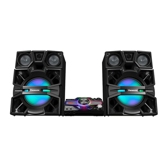
CD Stereo System
SA-MAX9000GM
SA-MAX9000GS
PSG1604007AE
PAGE
Advertisement
Table of Contents

Related Manuals for Panasonic SA-MAX9000 Series


Summary of Contents for Panasonic SA-MAX9000 Series
-
Page 1: Table Of Contents
2.5. Safety Parts Information -------------------------------- 6 5.5. Tuner Circuit----------------------------------------------- 15 3 Specifications ----------------------------------------------------- 7 5.6. Panel Circuit----------------------------------------------- 16 5.7. Mic Circuit-------------------------------------------------- 17 4 Block Diagram----------------------------------------------------- 9 © Panasonic Corporation 2016. All rights reserved. Unauthorized copying and distribution is a violation of law. - Page 2 5.8. USB Circuit ------------------------------------------------ 18 5.9. SMPS Circuit ---------------------------------------------- 19 6 Printed Circuit Board ------------------------------------------ 20 6.1. Main P.C.B. (Side A)------------------------------------- 20 6.2. Main P.C.B. (Side B)------------------------------------- 21 6.3. Tuner, Mic and USB P.C.B. ---------------------------- 22 6.4. Panel P.C.B. ----------------------------------------------- 23 6.5.
-
Page 3: Notes
1 Notes This simplified service manual is base on SA-MAX9000GN/PU (Order No. PSG1602004CE). 1) This service manual contains only following information - Safety Precautions - Specifications - Block Diagram - Schematic Diagram - Printed Circuit Board - Exploded View and Replacement Parts List 2 Safety Precautions 2.1. -
Page 4: Before Repair And Adjustment
2.1.2. Leakage Current Hot Check 1. Plug the AC cord directly into the AC outlet. Do not use an isolation transformer for this check. 2. Connect a 1.5k, 10 watts resistor, in parallel with a 0.15F capacitors, between each exposed metallic part on the set and a good earth ground such as a water pipe, as shown in Figure 1-1. -
Page 5: Caution For Ac Cord
2.4. Caution For AC Cord Figure 1-3... -
Page 6: Safety Parts Information
2.5. Safety Parts Information Safety Parts List: There are special components used in this equipment which are important for safety. These parts are marked by in the Schematic Diagrams, Exploded View & Replacement Parts List. It is essential that these critical parts should be replaced with manufacturer’s specified parts to prevent shock, fire or other hazards. -
Page 7: Specifications
3 Specifications Super Woofer 38 cm cone type x 1 High 3 / Mid 3 / Low 5 Impedance Amplifier section Dimensions (W x H x D) RMS output power stereo mode Including speaker feet 572 mm x 782 mm x 528 mm High Ch Excluding speaker feet 572 mm x 774 mm x 528 mm... -
Page 9: Block Diagram
4 Block Diagram 4.1. Audio : CD SIGNAL LINE : TUNER/AUX/MIC SIGNAL LINE : OUTPUT SIGNAL LINE : AM SIGNAL LINE : FM SIGNAL LINE MIC DET2 CN1401 P1803 MIC DET2 MIC DET2 MIC DET1 CN1401 P1803 MIC DET1 TO SYSTEM CONTROL JK1403 MIC DET1 IC4005... - Page 10 : TUNER/AUX/MIC SIGNAL LINE : OUTPUT SIGNAL LINE : AM SIGNAL LINE : FM SIGNAL LINE : CD SIGNAL LINE SPEAKERS MAIN P.C.B. Q4505 AMPLIFIER JK4201 38 IN3 LEFT LOW JK4201 46 IN1 40 IN4 Q4506 AMPLIFIER 44 IN2 Q4502 AMPLIFIER Q4509 DC DET...
-
Page 11: Schematic Diagram
5 Schematic Diagram 5.1. Main (IO Expansion) Circuit SCHEMATIC DIAGRAM - 1 MAIN (IO EXPANSION) CIRCUIT : +B SIGNAL LINE : AUX/MIC SIGNAL LINE R1805 P1802 J0JYC0000656 USBLED_REC REM_IN REM_IN USBLED_PLAY1 LB1201 R1236 J0JYC0000656 PW_XSW3R3V PW_STBY3R3V C1804 SP_INT DGND 1000P PW_SW3R3V PW_SW3R3V R1226... -
Page 12: Main (Micon) Circuit
5.2. Main (Micon) Circuit SCHEMATIC DIAGRAM - 8 MAIN (MICON) CIRCUIT : CD SIGNAL LINE : TUNER/AUX/MIC SIGNAL LINE : +B SIGNAL LINE : -B SIGNAL LINE : USB SIGNAL LINE IO: MAIN (IO EXPANSION): SCHEMATIC DIAGRAM - 1 IC1003 FA: MAIN (FAN LED): SCHEMATIC DIAGRAM - 2 ~ 3 RFKWFX9000GM DS: MAIN (DSP): SCHEMATIC DIAGRAM - 4... -
Page 13: Main (Usb) Circuit
5.3. Main (USB) Circuit SCHEMATIC DIAGRAM - 14 MAIN (USB) CIRCUIT : +B SIGNAL LINE : USB SIGNAL LINE T9001 P9001 J0ZZB0000182 DGND D+ A USB1_D+ D- A USB1_D- DGND D+ B USB CIRCUIT D- B (CN6002) T9002 USB_REC_LED IN SCHEMATIC J0ZZB0000182 USB_PLAY1_LED DIAGRAM - 21... -
Page 14: Main (Aux) Circuit
5.4. Main (AUX) Circuit SCHEMATIC DIAGRAM - 15 MAIN (AUX) CIRCUIT : +B SIGNAL LINE : AUX SIGNAL LINE ANALOG_SEL LB4901 J0JYC0000656 PW_SW12R0V DI IO C4906 C4920 R4906 R4926 16V47 JK4951 QR4901 R4901 C4904 B1GBCFJJ0040 ANALOG_SEL2 SWITCH QR4902 R4902 B1GBCFJJ0040 8.2K R4905 SWITCH... -
Page 15: Tuner Circuit
5.5. Tuner Circuit SCHEMATIC DIAGRAM - 16 TUNER CIRCUIT : AM SIGNAL LINE : FM SIGNAL LINE : +B SIGNAL LINE : TUNER SIGNAL LINE C7006 R7009 2.2K RX7001 R7010 2.2K D1H81024A042 C7009 IC7001 C7011 VUEALLPT087 220P JK7001 AM/FM RADIO RECEIVER 19 18 C7008 C7010... -
Page 16: Panel Circuit
5.6. Panel Circuit SCHEMATIC DIAGRAM - 17 PANEL CIRCUIT : +B SIGNAL LINE DP6300 TO PANEL R6402 CIRCUIT (2/3) A2BB00000186 FL DISPLAY IR6301 REMOTE SENSOR R6300 R6301 C6312 R6323 PW_5V R6306 R6311 C6306 FL1_CS C6330 C6307 R6330 REM_IN R6326 R6310 R6309 R6303 FLGND... -
Page 17: Mic Circuit
5.7. Mic Circuit SCHEMATIC DIAGRAM - 20 MIC CIRCUIT : +B SIGNAL LINE : AUX/MIC SIGNAL LINE C1431 4700P R1417 4.7K C1425 0.01 C1429 C1428 R1413 C1432 R1414 50V0.1 50V4.7 50V4.7 C1430 C1426 R1415 50V1 C1424 R1416 50V1 IC1400 C1AB00003130 MIC AMPLIFIER R1421 VR1400... -
Page 18: Usb Circuit
5.8. USB Circuit SCHEMATIC DIAGRAM - 21 USB CIRCUIT : +B SIGNAL LINE : USB SIGNAL LINE R6101 R6106 C6101 470K JK6001 USB5V CN6002 USB_A_D- USB PORT A DGND (PLAY) D+ A USB_A_D+ D- A R6102 DGND DGND R6103 D+ B MAIN (USB) D- B CIRCUIT (P9001) -
Page 19: Smps Circuit
5.9. SMPS Circuit SCHEMATIC DIAGRAM - 23 SMPS CIRCUIT : +B SIGNAL LINE : -B SIGNAL LINE IC1601 C0DAZYY00039 TO SMPS SHUNT REGULATOR CIRCUIT (1/2) Q1404 D1203 B0ECNR000003 B3PBA0000579 FEEDBACK R1602 Q1701 B3PBA0000579 R1607 LB1201 FEEDBACK 2.2K J0JYC0000656 C1211 R1604 470P R1724 R1603... -
Page 20: Printed Circuit Board
6 Printed Circuit Board 6.1. Main P.C.B. (Side A) MAIN P.C.B. (REP5348CA) R4604 R8078 C4620 R4602 R4597 R4596 R4598 R4599 R4600 R4569 C4548 D4517 D4516 C4570 RL4501 D4502 R4525 R4566 R4533 D4503 C4542 D4504 R4531 D4501 R4532 D4515 R4521 R4536 R4526 D4514 R4530... -
Page 21: Main P.c.b. (Side B)
6.2. Main P.C.B. (Side B) MAIN P.C.B. (REP5348CA) ZJ8001 R4603 C4567 C4568 ZC8003* C4619 R8080 CN8001 P4501 P8503 1 2 3 4 5 6 7 8 9 10 11 12 13 C4560 (TO FAN UNIT(REAR)) C8052 C4254 Q8507 Q8506 C4555 Q8508 K8004 R8521... -
Page 22: Tuner, Mic And Usb P.c.b
6.3. Tuner, Mic and USB P.C.B. TUNER P.C.B. (REP5348CB) USB P.C.B. (REP5316BC) AM ANT FM ANT USB PORT A USB PORT B (PLAY) (REC/PLAY) JK7002 VA7001 LB7001 JK6001 JK6002 LB7002 JK7001 C7006 L7001 C7005 R7009 C7009 L7002 C7008 R6106 R6108 C7004 C7002 R7005... -
Page 23: Panel P.c.b
6.4. Panel P.C.B. PANEL P.C.B. (REP5316BA) S6205 S6216 (MEMORY/USB) (FWD) S6201 S6217 R6204 (POWER) (ALBUM/TRACK) W6086 R6200 R6216 S6215 R6214 S6221 S6204 (REW) S6220 S6218 (CD/RADIO/AUX) (BT PAIRING) (LATIN EQ) (MEMORY REC) R6203 S6222 (PLAY/PAUSE) R6221 R6219 S6223 (USB REC) (D.BASS) S6203 (TUNE MODE) -
Page 24: Smps P.c.b
6.5. SMPS P.C.B. SMPS P.C.B. (REP5317D) CN1852 F1001 Q1201 Q1202 Q1205 F1501 T10AH 250V P1001 T5AL 250V ZJ1004 ZA1003 ZA1002 D1201 Q1501 Q1502 R1208 R1209 R1207 C1211 ZA1201* R1516 R1517 HEATSINK D1504 D1505 ZA1501* AC IN ~ HEATSINK 220V-240V 50/60Hz L1001 T1501 LB1201... -
Page 25: Exploded View And Replacement Parts List
7 Exploded View and Replacement Parts List 7.1. Cabinet Parts Location 1 (NFC KIT ASS’Y) (MIC P.C.B.) CN1401 JK1402 JK1401 JK1403 VR1400 VR1401 10-3 10-2 10-4 10-5 10-1 10-2 CN6002 JK6001 (USB P.C.B.) JK6002 SA-MAX9000GM/GS CABINET DRAWING... -
Page 26: Cabinet Parts Location
7.2. Cabinet Parts Location 2 VR6201 IR6301 P6200 DP6300 (PANEL P.C.B.) VR6202 SA-MAX9000GM/GS CABINET DRAWING... -
Page 27: Cabinet Parts Location
7.3. Cabinet Parts Location 3 35 35 35 *HEATSINK JK7002 JK4951 P1501 JK4201 P1502 P9002 P1802 JK7001 P8503 P1804 (TUNER P.C.B.) (MAIN P.C.B.) P9001 P9003 P8502 P4501 P5002 CN8001 P1803 P5001 *HEATSINK *HEATSINK *HEATSINK (CD MECHANISM UNIT) T1401 *HEATSINK *ZC1002 (CD INTERFACE P.C.B.) CN7002 F1401... -
Page 28: Packaging
7.4. Packaging ACCESSORIES BAG AC CORD UNIT SB-MAX9000 AC CORD AC CORD OI BOOK AM LOOP ANTENNA F R O N T SA-MAX9000GM/GS FM INDOOR ANTENNA LEG RUBBER x 8 F R O N T POLYFOAM (BOTTOM LEFT) POLYFOAM (BOTTOM RIGHT) POLYFOAM (TOP LEFT) SC-MAX9000GM/GS POLYFOAM (TOP RIGHT) -
Page 29: Mechanical Replacement Part List
7.5. Mechanical Replacement Part List Safety Ref. Part No. Part Name & Qty Remarks Description RGL0840-Q PATTERN LIGHT Safety Ref. Part No. Part Name & Qty Remarks PIECE Description RGR0484B-A REAR PANEL RGW0450-K MIC VOLUME KNOB CABINET CHASSIS RGW0448A-K DJ TABLE RGW0457-1S VOLUME KNOB REE1730... - Page 30 Safety Ref. Part No. Part Name & Qty Remarks Description J0KD00000172 FERRITE CORE J0KG00000199 FERRITE CORE XTB3+12JFJK SCREW RXA0277 SMPS SHIELD PLATE UNIT J0KG00000011 FERRITE CORE RSC1341 SHIELD PLATE B TRAVERSE DECK RAE1052Z-V TRAVERSE ASS'Y (E.S.D) XTN2+6GFJ SCREW PACKING MATERI- RPG0S59 PACKING CASE RFKZAX9000GM...
-
Page 31: Electrical Replacement Part List
7.6. Electrical Replacement Part List Safety Ref. No. Parts No. Parts name & Description Remarks SA-MAX9000GN SA-MAX9000GM/GS PCB1 RFKV5315DA RFKV5348CA MAIN/NFC KIT ASS'Y PCB2 REP5315DB REP5348CB TUNER P.C.B (RTL) PCB3 RFKV5315DC RFKV5348CC NFC KIT ASS'Y PCB4 REP5316AA REP5316BA PANEL P.C.B (RTL) PCB5 REP5316AB... - Page 32 Safety Ref. No. Parts No. Parts name & Description Remarks SA-MAX9000GN SA-MAX9000GM/GS R1225 D0GBR00J0004 1/10W R1410 D0GBR00J0004 1/10W R6402 D0GBR00J0004 1/10W W6203 D0GDR00J0004 1/8W R1416 D0GB101JA065 1/10W R1419 D0GB104JA065 100K 1/10W R4912 D0GB123JA065 1/10W R4913 D0GB123JA065 1/10W R4916 D0GB123JA065 1/10W R4917 D0GB123JA065 1/10W...