Table of Contents
Advertisement
Quick Links
www.osram-os.com
Application Note No. AN149
Handling of the OSRAM OSTAR
Application Note
Abstract
The OSRAM OSTAR
highest luminance and are specially designed for projection
applications. Different versions and designs offer the best
implementation possible in the application. In addition to
thermal management, correct handling and processing of the
LEDs are essential for a successful application. This application
note provides a recommendation for the appropriate handling
and processing of the different versions of the LED family.
Further information:
AN053_Thermal management of OSRAM OSTAR
AN084_Projection with LED light sources
2020-06-04 | Document No.: AN149
®
Projection Power family LEDs offer
®
Projection Power
Valid for:
®
OSRAM OSTAR
Projection Power
®
Projection light sources
Author: Retsch Stefanie / Jiang, DeGen
1 / 18
Advertisement
Table of Contents

Related Manuals for Osram OSTAR Projection Power


Summary of Contents for Osram OSTAR Projection Power
- Page 1 Application Note No. AN149 ® Handling of the OSRAM OSTAR Projection Power Application Note Valid for: ® OSRAM OSTAR Projection Power Abstract ® The OSRAM OSTAR Projection Power family LEDs offer highest luminance and are specially designed for projection applications.
-
Page 2: Table Of Contents
(which must be removed before operation) is used. ® The design of the OSRAM OSTAR Projection light source is also focused on thermal optimization, as for the highest current density of max 6A/mm² efficient cooling is necessary. -
Page 3: Mechanical And Optical Design Resources
Education Professional Mechanical and optical design resources For detailed information about the mechanical dimensions of the OSRAM ® OSTAR Projection Power devices please refer to the detailed drawings available in the data sheet. To obtain CAD data and optical rayfile, please visit the “Optical Simulation / Ray Files + Package CAD Data”... -
Page 4: General Handling Recommendations
This tape also protects the LED during the soldering process and should be left in place until initial operation. ® Figure 1: Protective tape for deep blue, blue and amber colored OSRAM OSTAR Projection Power B. General Handling recommendations The use of any type of sharp objects should generally be avoided, since this can damage the component. -
Page 5: Precautions And Storage
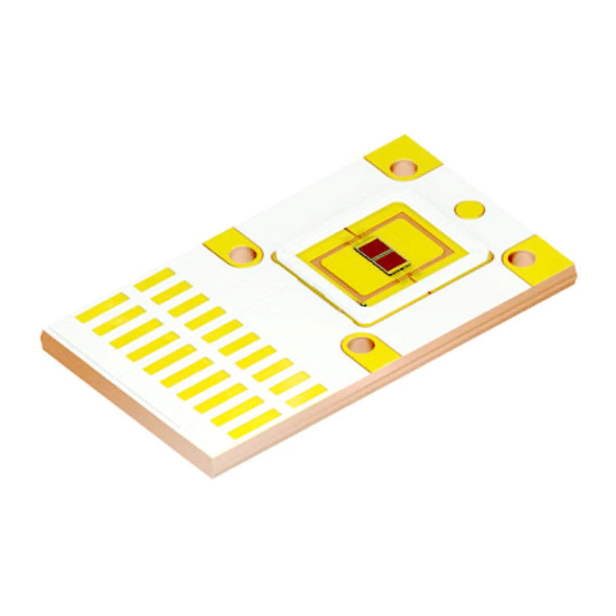
Level 2 (MSL 2) according to JEDEC J-STD- 020E. For more information please refer to the application note “Dry pack information”. As is the case for all LEDs from OSRAM Opto Semiconductors, the product also fulfills the current RoHS guidelines (European Union and China) and therefore contains no lead or other defined hazardous substances. - Page 6 This avoids losses due to cover reflectivity and stray light. Figure 4 shows an overview of all the devices of this class. ® Figure 4: Overview of new generation OSRAM OSTAR Projection Power with a connecting board LE CG P1AQ...
-
Page 7: Delivery
® The OSRAM OSTAR Projection Power devices on IMS-PCB (Insulated Metal Substrate) will be delivered on trays, like illustrated in Figure 6. OSRAM Opto Semiconductors can be contacted for a detailed drawing. Figure 6: Example of a tray Handling recommendations In addition to general guidelines on the handling of LEDs, additional care should be taken that mechanical tension on the carrier board and especially stress (e.g. - Page 8 Care should be taken that the light-emitting area is not touched or contaminated in any way. Figure 7 shows the critical area that should be not touched or contaminated. Figure 7: Keep out area Keep out, don‘t touch area...
-
Page 9: Assembly Of The Connector
For the connection to the heat sink, please use thermal interface material (for detailed information on thermal interface material, please refer to Application ® Note “AN053_Thermal management of OSRAM OSTAR Projection light sources”). The devices can be connected to the heat sink with a screw. - Page 10 Figure 10: Sketch of a possible carrier In order to obtain an effective soldering process, it is recommended to place the components with the pins opposite each other. Before solder paste printing can be performed, the component must be masked and the light-emitting part must be protected.
- Page 11 ® For the OSRAM OSTAR Projection Power, a standard reflow soldering process with forced convection can be applied. Since the soldering atmosphere and in particular air reflow can cause degradation of optical parameters it is advisable to use an N atmosphere (<500 ppm O...
- Page 12 Figure 14: Maximum and recommended solder temperature for soldering the connector to the PCB in accordance with to JEDEC J-STD-020E T [°C] 245 °C Recommended solder profile 240 °C (max 260 °C) 217 °C Ramp down 6 K/s (max)
-
Page 13: Osram Ostar ® Projection Power Smt
® D. OSRAM OSTAR Projection Power SMT OSRAM OSTAR® Projection Power SMT devices (LE x P0MQ/AQ) come with a copper substrate which offers lowest thermal resistance. These devices also comprise a large electrical isolated thermal pad for better thermal dissipation. -
Page 14: Handling Recommendations
Handling recommendations Please be aware of ESD safety while handling the LED (see Application Note “ESD protection while handling LEDs”). In addition to the general guidelines for the handling of LEDs, additional care should be taken that mechanical stress (e.g. -
Page 15: Solder Pad Design
Figure 18: Recommended pick-and-place nozzle from ASM SIPLACE SIPLACE Nozzle 3081899 Solder pad design Since the solder pad effectively creates the direct contact between the LED and the circuit board, the design of the solder pad contributes decisively to the performance of the solder connection. -
Page 16: Solder Stencil
Proper solder paste printing increases the solder quality. Effects such as solder bridges, solder balling, solder spray and/or other soldering defects are largely determined by the design of the stencil apertures and the quality of the stencil printing (e.g. positioning, cleanliness of the stencil, etc.). For the OSRAM ® OSTAR Projection Power a stencil thickness of 120 μm is recommended. - Page 17 Figure 21: Temperature profile for lead-free reflow soldering in accordance with JEDEC J-STD-020E T [°C] 245 °C Recommended solder profile 240 °C (max 260 °C) 217 °C Ramp down 6 K/s (max) up to 30 s up to 120 s...
- Page 18 Regensburg (Germany), Penang (Malaysia) and Wuxi (China). Its headquarters for North America is in Sunnyvale (USA), and for Asia in Hong Kong. OSRAM Opto Semiconductors also has sales offices th- roughout the world. For more information go to www.osram-os.com.
Need help?
Do you have a question about the OSTAR Projection Power and is the answer not in the manual?
Questions and answers