Table of Contents
Advertisement
Quick Links
Notes: This model's CD Mechanism Unit is CR14C. Please refer to the original service manual
(Order No. MD0805031CE) for this mechanism
TABLE OF CONTENTS
1 Safety Precautions----------------------------------------------- 3
1.1. General Guidelines---------------------------------------- 3
1.2. Before Use (For PU only)-------------------------------- 3
1.3. Before Repair and Adjustment ------------------------- 3
1.4. Protection Circuitry ---------------------------------------- 4
1.5. Safety Parts Information --------------------------------- 4
2 Warning -------------------------------------------------------------- 6
Model No.
Product Color: (K)...Black Type
PAGE
to Electrostatic Sensitive (ES) Devices---------------6
2.2. Precaution of Laser Diode -------------------------------7
2.4. Handling Precautions for Traverse Unit --------------9
3 Service Navigation --------------------------------------------- 11
3.1. Service Information -------------------------------------- 11
4 Specifications ---------------------------------------------------- 12
© Panasonic Corporation 2009. All rights reserved.
Unauthorized copying and distribution is a violation
of law.
CD Stereo System
SA-AK180PN
SA-AK180PU
PSG0905023CE
PAGE
Advertisement
Table of Contents

Related Manuals for Panasonic SA-AK180PN


Summary of Contents for Panasonic SA-AK180PN
-
Page 1: Table Of Contents
1.5. Safety Parts Information --------------------------------- 4 3 Service Navigation --------------------------------------------- 11 2 Warning -------------------------------------------------------------- 6 3.1. Service Information -------------------------------------- 11 4 Specifications ---------------------------------------------------- 12 © Panasonic Corporation 2009. All rights reserved. Unauthorized copying and distribution is a violation of law. - Page 2 5 Location of Controls and Components------------------ 13 11.7. SMPS P.C.B.---------------------------------------------- 61 5.1. Main Unit Key Button Operation---------------------- 13 11.8. Waveform Table (1/2)----------------------------------- 62 5.2. Remote Control Key Button Operation ------------- 14 11.9. Waveform Table (2/2)----------------------------------- 63 5.3. Disc Information ------------------------------------------ 15 12 Illustration of ICs, Transistor and Diode ---------------- 64 6 Self-Diagnosis and Special Mode Setting -------------- 16 13 Block Diagram --------------------------------------------------- 65...
-
Page 3: Safety Precautions
1 Safety Precautions 1.1. General Guidelines 1. When servicing, observe the original lead dress. If a short circuit is found, replace all parts which have been overheated or damaged by the short circuit. 2. After servicing, see to it that all the protective devices such as insulation barriers, insulation papers shields are properly installed. -
Page 4: Protection Circuitry
1.3.1. Caution for fuse replacement 1.4. Protection Circuitry The protection circuitry may have operated if either of the following conditions are noticed: • No sound is heard when the power is turned on. • Sound stops during a performance. The function of this circuitry is to prevent circuitry damage if, for example, the positive and negative speaker connection wires are “shorted”, or if speaker systems with an impedance less than the indicated rated impedance of the amplifier are used. - Page 5 Safety Ref. No. Part No. Part Name & Description Remarks TH5860 D4CC11040013 THERMISTOR P5701 K2AA2B000017 AC INLET P5701 K2AB2B000011 AC INLET C5700 F1BAF1020020 1000pF C5701 F0CAF334A087 0.33uF C5703 F0C2H1040001 0.1uF 500V C5703 F0CAF224A085 0.22uF C5704 F1BAF1020020 1000pF C5705 F1BAF1020020 1000pF C5706 F1BAF1020020 1000pF...
-
Page 6: Warning
2 Warning 2.1. Prevention of Electrostatic Discharge (ESD) to Electrostatic Sensitive (ES) Devices Some semiconductor (solid state) devices can be damaged easily by static electricity. Such components commonly are called Elec- trostatically Sensitive (ES) Devices. Examples of typical ES devices are integrated circuits and some field-effect transistors and semiconductor "chip"... -
Page 7: Precaution Of Laser Diode
2.2. Precaution of Laser Diode Caution: This product utilizes a laser diode with the unit turned “on”, invisible laser radiation is emitted from the pickup lens. Wavelength: 785 nm (CD) Maximum output radiation power from pickup: 100 µW/VDE Laser radiation from the pickup unit is safety level, but be sure the followings: 1. -
Page 8: Service Caution Based On Legal Restrictions
2.3. Service caution based on Legal restrictions 2.3.1. General description about Lead Free Solder (PbF) The lead free solder has been used in the mounting process of all electrical components on the printed circuit boards used for this equipment in considering the globally environmental conservation. The normal solder is the alloy of tin (Sn) and lead (Pb). -
Page 9: Handling Precautions For Traverse Unit
2.4. Handling Precautions for Traverse Unit The laser diode in the optical pickup unit may break down due to static electricity of clothes or human body. Special care must be taken avoid caution to electrostatic breakdown when servicing and handling the laser diode in the traverse unit. Cautions to Be Taken in Handling the Optical Pickup Unit 2.4.1. - Page 10 2.4.2.2. Human body grounding 1. Use the anti-static wrist strap to discharge the static electricity form your body.
-
Page 11: Service Navigation
3 Service Navigation 3.1. Service Information This service manual contains technical information which will allow service personnel’s to understand and service this model. Please place orders using the parts list and not the drawing reference numbers. If the circuit is changed or modified, this information will be followed by supplement service manual to be filed with original service manual. -
Page 12: Specifications
4 Specifications 2. Total harmonic distortion is measured by the digital spectrum analyzer. System: SC-AK180PN-K Main Unit: SA-AK180PN-K Speaker System: SB-AK280PN-K Main unit SA-AK180PN/PU-K System: SC-AK180PU-K Main Unit: SA-AK180PU-K AMPLIFIER SECTION Speaker System: SB-AK280PN-K RMS Output Power Stereo Mode Front CH (both channels driven): 125 W per channel (3 Ω), 1 kHz, 10% THD... -
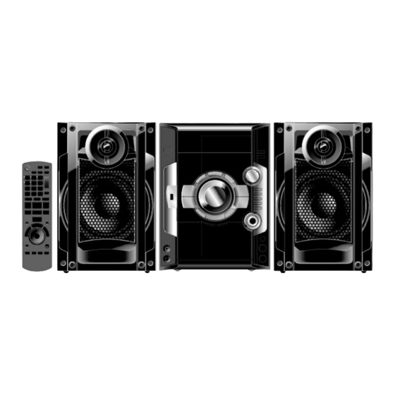
Page 13: Location Of Controls And Components
5 Location of Controls and Components 5.1. Main Unit Key Button Operation MUSIC PORT Headphone jack Display Panel Reduce the volume level and connect the headphones. Disc Ttrays Headphones plug type : 3.5 mm stereo (not included). Avoid listening for prolonged periods of time to Standby/on switch ( prevent hearing damage. -
Page 14: Remote Control Key Button Operation
5.2. Remote Control Key Button Operation Play timer or record timer setting Select and play the other loaded discs. Sleep timer Numberic selection Auto off USB play or pause Delete function Muting function Program function Tuner (FM/AM) Selection FM selection Manual EQ selection Stop playback, demonstration function Volume Adjustment... -
Page 15: Disc Information
5.3. Disc Information NOTE about using a DualDisc The digital audio content side of a DualDisc does not meet the technical speci cations of the Compact Disc Digital Audio (CD-DA) format so playback may not be possible. NOTE on CDs This unit can access up to 99 tracks. -
Page 16: Self-Diagnosis And Special Mode Setting
6 Self-Diagnosis and Special Mode Setting This unit is equipped with features od self-diagnosis & special mode setting for checking the function & reliability. Special Note: Checking of the reliability (ageing) & changer operation must be carry out to ensure good working condition in unit. - Page 17 6.2. Doctor Mode Table Below is the various modes for checking:- 6.2.1. Doctor Mode Table 1 Item Key Operation FL Display Mode Name Description Front Key (Display 1) Doctor Mode To enter into Doctor Mode for checking In CD Mode: of variuos items and displaying 1.
-
Page 18: Doctor Mode Summary Table [Cd Mechanism Unit (Cr14C)]
6.2.2. Doctor Mode Table 2 Item Key Operation FL Display Mode Name Description Front Key Cold Start To active cold start upon next AC In Doctor mode: power up when reset start is execute 1. Press [4] button on the next time. remote control. -
Page 19: Service Mode Table [Cd Mechanism Unit (Cr14C)]
6.4. Service Mode Table [CD Mechanism Unit (CR14C)] Item Key Operation FL Display Mode Name Description Front Key Self-Diagnostic To enter into self-diagnostic checking In AUX mode (ensure no disc is Mode for CR14C mechanism. inserted): Press and hold [STOP] button for 2 seconds, followed by [ /FF/ button on the main unit. -
Page 20: Reliability Test Mode (Cd Mechanism Unit Cr14C)
6.5. Reliability Test Mode (CD Mechanism Unit CR14C) Below is the progress flow chart of ageing for the Mechanism unit (CR14C). Fig. 1 Fig. 2... - Page 21 Fig. 3 Fig. 4...
- Page 22 Fig. 5...
-
Page 23: Error Code Table
6.6. Error Code Table Self-Diagnosis Function (refer Section “6.” Service Mode Table 1”) provides information on any problems occurring for the unit and its respective components by displaying the error codes. These error code such as U**, H** and F** are stored in memory and held unless it is cleared. - Page 24 6.6.2. Error Code Table (For Power Supply) Error Code Diagnosis Contents Description of error Automatic FL Display Remarks Power Amp IC output Upon power For power. abnormal PCNT=HIGH, DCDET2=L Press [ ] on main unit for -DEMO after checking LSI. next error.
-
Page 25: Troubleshooting Guide
7 Troubleshooting Guide 7.1. Troubleshooting Guide for F61 and/or F76 This section illustrates the checking procedures when upon detecting the error of “F61” and/or “F76” after power up of the unit. It is for purpose of troubleshooting and checking in SMPS, D-Amp & Main P.C.B. 7.1.1. - Page 26 7.1.2. Troubleshooting Guide Symptom Checking Items Repair Items Remarks Check the soldering of the SMPS Tou ch-up the solder crack area/ FL display blinking with SMPS P. C.B. Change the defective parts. abnormal segment when P. C.B. Is there any solder crack at area Q5860,Q5861,Q5862,TH5860 power ON the set or "F61"...
- Page 27 7.1.3. Part Location 7.1.3.1. SMPS P.C.B. Feedback circuit: PC5720, D5725 -30V Detect: QR5801, QR5802, Temperature Detect: Q5860, Q5681, Q5862 Temperature Detect: TH5860 Feedback Circuit: IC5801, Q5802, D5806 SMPS P.C.B. Fig. 1 SMPS P.C.B.
- Page 28 7.1.3.2. D-Amp P.C.B. Audio Digital Power Amp IC: IC5000 Muting Circuit Q5601, Q5604 D-Amp P.C.B. Fig. 2 D-Amp P.C.B.
- Page 29 7.1.3.3. Main P.C.B. +12V Regulator IC: IC2731 Connector: CN2806 Switching Regulator IC: IC2701 Fuse Protector: FP2901 T2900, D2901, D2906, D2908 & D2909 Main P.C.B. Fig. 3 Main P.C.B.
-
Page 30: Service Fixture & Tools
8 Service Fixture & Tools 8.1. Service Tools and Equipment Prepare service tools before process service position. Service Tools Remarks Main P.C.B. (CN2341A) - D-Amp P.C.B. (CN5050) REEX0930 (17P FFC) (RTL) Main P.C.B. (CN2701) - SMPS P.C.B. (CN5802) REEX0680 (11P wire) (RTL) SMPS P.C.B. -
Page 31: Disassembly And Assembly Instructions
9 Disassembly and Assembly Instructions “ATTENTION SERVICER” Be careful when disassembling and servicing. Some chassis components may have sharp edges. Special Note: 1. This section describes the disassembly procedures for all the major printed circuit boards and main components. 2. Before the disassembly process was carried out, do take special note that all safety precautions are to be carried out. -
Page 32: Disassembly Flow Chart
9.1. Disassembly Flow Chart 9.3. Top Cabinet 9.23. Voltage Selector 9.4. CD Mechanism Unit 9.20. AC Inlet P.C.B. P.C.B. (For PU only) (CR14C) 9.24.Traverse Unit 9.5. Rear Panel Assembly 9.6. Front Panel 9.10. CD Servo P.C.B. Assembly 9.11.D-Amp P.C.B. 9.7. Panel P.C.B. 9.8. -
Page 33: Main Components And P.c.b. Locations
9.2. Main Components and P.C.B. Locations... -
Page 34: Disassembly Of Top Cabinet
9.3. Disassembly of Top Cabinet Step 1: Remove 3 screws on each side. Step 4: Push the Top Cabinet backwards as arrow shown to release the catches. Step 2: Remove 5 screws. Step 5: Remove the Top Cabinet. 9.4. Disassembly of CD Mecha- nism Unit (CR14C) •... - Page 35 Step 4: Release claws outwards on both sides. Step 1: Remove 1 screw. Step 2: Detach 22P FFC at the connector (CN2801) on Main P.C.B. Step 3: Detach 11P FFC at the connector (CN2805) on Main P.C.B. Step 5: Release the CD Mechanism Unit (CR14C) from the catches &...
-
Page 36: Disassembly Of Rear Panel
Caution: During assembling, ensure the CD Mechanism Unit (CR14C) is seated properly on the locators. Step 7: Remove 2 screws. Step 8: Remove the CD Mechanism Unit (CR14C). 9.5. Disassembly of Rear Panel • Follow (Step 1) to (Step 5) of Item 9.3 •... -
Page 37: Disassembly Of Front Panel Assembly
Step 3: Slightly lift up the CD Mechanism Unit (CR14C) to Step 3: Detach 8P FFC at the connector (CN2807) on Main release from the 2 locators. P.C.B. Step 4: Detach Voltage Selector from Rear Panel as arrow Step 4: Detach 2P wire at the connector (CN2001) on Main shown. -
Page 38: Disassembly Of Panel P.c.b
Caution: During assembling, ensure both the claws and catches are fully catched. Step 1: Remove Volume Knob. Step 2: Remove Track Knob. Step 7: Release tabs at the bottom. Caution: Do not exert strong force when releasing the tabs. Step 3: Remove 8 screws on Panel P.C.B. Step 4: Remove 1 screw on Support P.C.B. -
Page 39: Disassembly Of Dynamic Bass Knob & Dynamic Bass Button Unit
9.8.1. Disassembly Dynamic Bass Knob Step 1: Release 4 catches. Step 5: Release 8 catches. Step 6: Remove Panel P.C.B. Step 2: Remove the Dynamic Bass Knob Assembly. Caution: During assembling of Panel P.C.B., ensure that the diodes on Panel P.C.B. are in upright position. 9.8. - Page 40 Caution 1: Do not misplace the Volume Gear. Caution 2: Volume gear to align to Volume Knob & engage to Dynamic Bass Knob during assembly. 9.8.2. Disassembly of Dynamic Bass But- ton Unit Step 3: Release 3 catches. Step 4: Remove the Dynamic Bass Knob. Step 1: Release 4 catches.
-
Page 41: Disassembly Of Cd Lid
Step 1: Upset the CD Mechanism Unit (CR14C). Step 3: Remove the Dynamic Bass Button Unit. 9.9. Disassembly of CD Lid • Follow (Step 1) to (Step 5) of Item 9.3 • Follow (Step 1) to (Step 8) of Item 9.6 Step 2: Desolder 4 solder points. -
Page 42: Disassembly Of D-Amp P.c.b
Step 4: Flip over the CD Servo P.C.B.. Step 5: Detach the 16P FFC at connector (CN7001) at CD Servo P.C.B.. Step 6: Remove the CD Servo P.C.B.. 9.11. Disassembly of D-Amp P.C.B. • Follow (Step 1) to (Step 5) of Item 9.3 •... -
Page 43: Replacement Of Audio Digital Power Amp Ic (Ic5000)
Step 5: Lift up the D-Amp P.C.B. together with inner chassis Caution: During assembling, ensure the D-Amp P.C.B. is assembly as arrow shown. seated properly on the locator of the Inner Chassis. 9.12. Replacement of Audio Digital Power Amp IC (IC5000) •... -
Page 44: Disassembly Of Main P.c.b
screwing of TR Spring. Caution: Ensure pins of the Audio Digital Power Amp IC (IC5000) are properly seated and soldered on D-Amp P.C.B. 9.13. Disassembly of Main P.C.B. • Follow (Step 1) to (Step 5) of Item 9.3 • Follow (Step 1) to (Step 6) of Item 9.4 •... -
Page 45: Disassembly Of Smps P.c.b
Step 4: Flip the SMPS P.C.B. and desolder the wire’s pin. Caution: Red and Black wires (For PN only). Caution: Red, Black, Blue wires (For PU only). Step 3: Remove 2 screws on at bottom chassis. Step 4: Remove the Main P.C.B. as arrow shown. 9.14. -
Page 46: Replacement Of Rectifier Diode (D5702)
Step 1: Apply grease to the Heatsink Unit B. Step 2: Mount the Switching Regulator IC (IC5701) on to SMPS P.C.B. Caution Ensure pins of the Switching Regulator IC (IC5701) are properly seated on SMPS P.C.B. Step 1: Desolder pins of the Switching Regulator IC (IC5701) on the solder side of SMPS P.C.B. - Page 47 Caution: During replacement of the part, avoid touching the heatsink, it may lead to injuries. 9.16.2. Assembly of Rectifier Diode (D5702) Step 1: Desolder pins of the Rectifier Diode (D5702) on the sol- Step 1: Apply grease to the Heatsink Unit B. der side of SMPS P.C.B.
-
Page 48: Replacement Of Regulator Diode (D5801)
Step 6: Solder pins of the Heatsink Unit B on the solder side of Caution: During replacement of the part, avoid touching SMPS P.C.B. the heatsink, it may lead to injuries. 9.17.2. Assembly of Regulator Diode 9.17. Replacement of Regulator (D5801) Diode (D5801) •... -
Page 49: Replacement Of Regulator Diode (D5803)
Caution: Ensure the Regulator Diode (D5802) is well tight- ened to the heatsink unit C. Step 1: Desolder pins of the Regulator Diode (D5802) on the solder side of SMPS P.C.B. Step 3: Solder pins of the Regulator Diode (D5802) on the sol- der side of SMPS P.C.B. -
Page 50: Disassembly Of Ac Inlet P.c.b
Caution: Ensure pins of the regulator diode (D5803) are properly seated and soldered on SMPS P.C.B. 9.20. Disassembly of AC Inlet P.C.B. • Follow (Step 1) to (Step 5) of Item 9.3 Step 2: Remove 1 screw. Step 3: Remove the Regulator Diode (D5803) from the Heat- sink Unit C. -
Page 51: Disassembly Of Usb P.c.b
Caution: (For PN only) Remember to use tie wraps to tie Caution: During assembling, ensure the AC Inlet P.C.B. is the red, black wires to the bottom chassis as diagram seated properly at the locators. show. Caution: (For PN only) Remember to use tie wraps to tie Caution: (For PU only) Remember to use tie wraps to tie the red, black wires to the bottom chassis as diagram the red, black, blue wires to the bottom chassis as diagram... -
Page 52: Disassembly Of Mport/Headphone P.c.b
Step 4: Remove USB P.C.B. 9.22. Disassembly of MPort/Head- phone P.C.B. • Follow (Step 1) to (Step 5) of Item 9.3 • Follow (Step 1) to (Step 8) of Item 9.6 Step 1: Remove 1 screw. Step 1: Remove 1 screw. Step 2: Release 2 catches. -
Page 53: Replacement Of Traverse Unit Assembly
Caution: Disassembly of Traverse Unit Assembly in play position. Step 1: Release the catch and push the guide as arrows shown to open both grooves. Step 3: Desolder blue wire pin & white wire pin on the Voltage Selector P.C.B. Step 4: Remove the Voltage Selector P.C.B. - Page 54 Caution: Ensure the bosses fix exactly onto the guides. Step 2: Place down the Traverse Unit Assembly. Step 3: Fix the FFC wires by using the adhesive tape. Step 3: Remove the Traverse Unit Assembly as arrows shown. 9.24.2. Assembly of Traverse Unit Assem- Step 4: Release the catch and push the guide as arrows shown to close both grooves.
-
Page 55: Service Position
10 Service Position Note: For description of the disassembly procedures, see the Section 9. 10.1. Checking and Repairing of Main P.C.B. • Follow (Step 1) to (Step 5) of Item 9.3 Step 4: Connect 8P FFC at the connector (CN2807) on Main P.C.B. -
Page 56: Checking And Repairing Of Smps And Ac Inlet P.c.b
Step 1: Position Mechanism Unit (CR14C) according to the dia- gram show. Step 2: Connect 11P FFC at the connector (CN2805) on Main Step 1: Position SMPS P.C.B., AC Inlet P.C.B. & Voltage Selec- P.C.B. tor P.C.B. as diagram shown. Step 3: Connect 22P FFC at the connector (CN2801) on Main Step 2: Connect 11P FFC at the connector (CN2805) on Main P.C.B. -
Page 57: Voltage & Waveform Chart
STANDBY IC7001 REF NO. MODE CD PLAY STANDBY IC7001 REF NO. MODE CD PLAY STANDBY REF NO. IC7002 MODE CD PLAY STANDBY IC7002 REF NO. MODE CD PLAY STANDBY Q7601 REF NO. MODE CD PLAY STANDBY SA-AK180PN/PU CD SERVO P.C.B. -
Page 58: Main P.c.b. (1/2)
CD PLAY STANDBY IC2801 REF NO. MODE CD PLAY STANDBY IC2801 REF NO. MODE CD PLAY STANDBY IC2801 REF NO. MODE CD PLAY STANDBY REF NO. IC2803 MODE CD PLAY STANDBY IC2803 REF NO. MODE CD PLAY STANDBY SA-AK180PN/PU MAIN P.C.B. -
Page 59: Main P.c.b. (2/2)
STANDBY 16.0 -0.3 Q3002 QR2317 REF NO. MODE CD PLAY -7.6 STANDBY SA-AK180PN/PU MAIN P.C.B. 11.4. Panel P.C.B. IC6601 REF NO. MODE CD PLAY -20.4 16.5 24.3 -24.3 -24.3 -22.4 -18.5 STANDBY -10.7 14.5 14.5 -24.3 -22.4 -22.4 -18.5 IC6601 REF NO. -
Page 60: Usb P.c.b
CD PLAY STANDBY IC900 REF NO. MODE CD PLAY STANDBY IC900 REF NO. MODE CD PLAY STANDBY SA-AK180PN/PU USB P.C.B. 11.6. D-Amp P.C.B. IC5000 REF NO. MODE CD PLAY 29.0 -29.0 -20.6 29.3 -29.3 -19.2 -29.3 -0.1 29.3 -29.0 -29.0 29.0 STANDBY 29.0... -
Page 61: Smps P.c.b
MODE CD PLAY 19.9 19.9 19.2 17.0 -21.9 -2.2 -22.0 STANDBY 19.9 19.9 19.2 16.8 -21.8 -2.2 -22.0 REF NO. Q5860 Q5861 Q5862 Q5898 QR5801 MODE CD PLAY STANDBY QR5802 QR5810 REF NO. MODE CD PLAY STANDBY SA-AK180PN/PU SMPS P.C.B. -
Page 62: Waveform Table (1/2)
11.8. Waveform Table (1/2) 3.1Vp-p(20nsec/div) 2.1Vp-p(20nsec/div) 2.2Vp-p(1msec/div) 2Vp-p(500usec/div) 3.2Vp-p(1msec/div) 0.4Vp-p(200usec/div) 3Vp-p(1msec/div) 3Vp-p(200usec/div) 0.56Vp-p(1msec/div) 0.6Vp-p(1msec/div) 1.9Vp-p(200usec/div) 0.6Vp-p(200usec/div) 2Vp-p(500usec/div) 5Vp-p(200usec/div) 5.6Vp-p(1usec/div) 1.4Vp-p(1msec/div) 80Vp-p(1usec/div) 6.8Vp-p(500nsec/div) 5.6Vp-p(500nsec/div) 1.5Vp-p(500usec/div) -
Page 63: Waveform Table (2/2)
11.9. Waveform Table (2/2) 5.8Vp-p(500nsec/div) 2Vp-p(5usec/div) 2Vp-p(5usec/div) 400Vp-p(2usec/div) 9.6Vp-p(5usec/div) 240Vp-p(50usec/div) 1.65Vp-p(5msec/div) 1.5Vp-p(1usec/div) -
Page 64: Illustration Of Ics, Transistor And Diode
12 Illustration of ICs, Transistor and Diode C0JBAB000902 (14P) C0DBGYY00089 (5P) C0AABB000125 (8P) RFKWEAK180PN (8P) C1AB00003093 (52P) C0HBB0000057 (44P) MNZSFB5KJM2 (64P) MN6627954AMA (100P) RFKWMAK180PN (100P) AN7326K (22P) BA5948FPE2 C0CAAKG00046 C1BA00000492 (23P) C0DABFC00002 (3P) C0DAAYG00001 C0DAEMZ00001 (3P) C5HACYY00004 (7P) B1BACD000018 B1BACG000023 2SC3940ARA B1ACKD000006 MIP4110MSSCF... -
Page 65: Block Diagram
SHIFT CN7001 CN7001 TRV GAIN 24 TRP [CH4] LEVEL SHIFT CN7001 [CH2] 23 TRVP LEVEL TRAVERSE SHIFT MOTOR [CH1] 21 SPOUT LEVEL SPINDLE SHIFT MOTOR MUTE [CH1] 22 PC MUTE [CH2] CN7002 CN2801 MAIN (1/2) SA-AK180PN/PU CD SERVO BLOCK DIAGRAM... -
Page 66: Main (1/2)
CN2806 CN6001 32 IPOD RXD KEY2 CN2811 34 BUSY MUSIC PORT FM/AM MANUAL EQ+ MANUAL EQ MANUAL EQ- S6307 S6306 S6305 S6304 S6303 S6302 S6301 S6300 CN2811 12 /RESET Q2812 CN2806 CN6001 RESET VREF KEY3 SA-AK180PN/PU MAIN (1/2) BLOCK DIAGRAM... -
Page 67: Main (2/2)
19 SDA MAIN (1/2) CN2807 CN6807 QR2317 Q2359 FROM MUTING MUTING MUTE A MAIN (1/2) CONTROL JK6810 CN6807 CN2807 52 MP R PRE-OUT-R CN6807 CN2807 MUSIC PORT 40 MP L REC-R PRE-IN-R REC-L PRE-IN-L PRE-OUT-L SA-AK180PN/PU MAIN (2/2) BLOCK DIAGRAM... -
Page 68: D-Amp
IN2M CN2341A CN5050 FRONT L FROM MAIN (2/2) - 30V SENSE IC5500 C0JBAB000902 INVERTER GATE (CLOCK GENERATOR) D5501 CN5050 FHOP CN2341A X5501 X5500 FAN DC D5502 FROM/TO MAIN (1/2) Q5101,Q5102 CN2341A CN5050 DC DET DC DETECT SA-AK180PN/PU D-AMP BLOCK DIAGRAM... -
Page 69: Power
+ 30V SENSE 7, 8 D5801 CN5500 H5801* - 30V SENSE - 30V SENSE 3, 4 IC5801 C0DABFC00002 SHUNT REGULATOR Q5802, D5806 PC5720 FEED BACK FEED BACK CIRCUIT Q5803 FROM CN2701* CN5802 AMBP SWITCHING MAIN (1/2) SA-AK180PN/PU POWER BLOCK DIAGRAM... -
Page 70: Wiring Connection Diagram
CN7002 MAIN P.C.B. TO CR14C T2900 MECHANISM UNIT (SOLDER SIDE) T5701 (MAIN TRANSFORMER) (SWITCHING T5751 TRANSFORMER) (SUB TRANSFORMER) TO OPTICAL PICKUP UNIT CN2001 CN2806 CN3200 CN2807 FOR SOFTWARE NOTE: " * " REF IS FOR INDICATION ONLY. SA-AK180PN/PU WIRING CONNECTION... -
Page 71: Schematic Diagram Notes
15 Schematic Diagram Notes • Voltage and signal line : +B signal line • This schematic diagram may be modified at any time : -B signal line with the development of new technology. : CD Audio input signal line Notes: : AUX/M.Port input Audio signal line S5701: Voltage Selector switch (For PU only). -
Page 73: Schematic Diagram
C7243 C7155 IODD2 R7329 SDRCK DVSS1 X7201 H0H169500013 R7328 21 20 15 14 12 11 C7335 C7334 10V220 R7323 R7331 6.8K IC7002 BA5948FPE2 R7325 R7315 3.3K 4CH DRIVER R7332 R7335 SA-AK180PN/PU CD SERVO CIRCUIT M7301* M7302* TRAVERSE MOTOR SPINDLE MOTOR... -
Page 74: Main Circuit
VOLTAGE REGULATOR Q2812 CN2001 SYS6V B1GBCFLL0037 MPORT/HEADPHONE C2813 R2744 RESET 50V3.3 4.7K CIRCUIT (ZJ6801*) IN SCHEMATIC DIAGRAM - 11 D2812 R2611 C2611 Q2745 MA2J1110GL B1GBCFLL0037 POWER CONTROL DGND TO MAIN C2960 SECTION (2/4) SA-AK180PN/PU MAIN CIRCUIT TO MAIN SECTION (3/4) - Page 75 B1BABK000001 UD_SENSOR TO CR14C UD_SENSOR PSAVE CONTROL CHG_CW LD_CW CHG_CCW LD_CCW R2902 CLOSE_SW C2901 3900P D2906 CLOSE_SENSOR B0JAME000114 HOME_SW HOME_SW OPEN_SW OPEN_SW R2680 R2667 R2668 R2669 VREF+ R2672 R2673 TO MAIN SECTION (1/4) SA-AK180PN/PU MAIN CIRCUIT TO MAIN SECTION (4/4)
- Page 76 AUDIO SIGNAL PROCESSOR B1GFGCAA0001 MUTING CONTROL I_PORTR MUTING CONTROL ROUT DC-DC_GND ROUT AUX_R C2086 C2305 50V3.3 C2312 R2312 AUX_R PA_IN_R R2062 C2066 MP_R ASP_CLK USB+5V R2302 470K ASP_DA 11 12 PCONT CD/USB_R C2046 +9VASP TUNER_R C2026 R2303 R2305 A_GND SA-AK180PN/PU MAIN CIRCUIT...
- Page 77 DET_OUT DC18V L2911 G0C330JA0055 +9VASP C3805 TUNER_GND TU_GND C2093 MOTOR_12V 0.01 IC2731 2091 C0CAAKG00046 Q2735 CHASSIS GND +12V REGULATOR B1BACD000018 D2732 B0EAKM000117 +7.5V REGULATOR JK2801 +7.5V [LCH] R2083 5.6K AUX_L SA-AK180PN/PU A_GND MAIN CIRCUIT [RCH] R2735 R2084 5.6K AUX_R MOTOR_GND...
-
Page 78: Panel Circuit
100P S6302 MANUAL EQ + 3 2 1 VR6500 EVEKE2F3524B S6301 VOLUME JOG MANUAL EQ S6300 MANUAL EQ - R6884 C6633 C6634 R6882 100P 100P 3 2 1 VR6630 VR6882 K9AA012Y0003 K9AA012Y0002 BASS CONTROL JOG TRACK JOG SA-AK180PN/PU PANEL CIRCUIT... -
Page 79: Usb Circuit
J0JBC0000033 MAIN CIRCUIT CD_DATA (CN3200) DGND IN SCHEMATIC LB840 J0JBC0000033 STCLK DIAGRAM - 2 TERR LB841 J0JBC0000033 STREQ LB843 J0JBC0000033 STIN LB845 J0JBC0000033 CD_MLD LB846 J0JBC0000033 CD_NRST LB848 J0JBC0000033 M_NRST DGND SA-AK180PN/PU USB CIRCUIT LB850 D3.3V MMOD R903 DGND DGND... -
Page 80: D-Amp Circuit
R5506 H2A7003A0011 C5551 390P K5256 Q5102 C5553 100P B1ABCF000176 X5500 R5507 H2A6023A0011 DC DETECT C5552 390P R5505 R5020 FR_+ Q5101 FL_+ R5019 B1ABCF000176 DC DETECT R5602 R5671 Q5604 MOD_DA B1ABCF000176 R5609 SWITCH MUTE F_SW Q5601 B1ABCF000176 SWITCH SA-AK180PN/PU D-AMP CIRCUIT... -
Page 81: Smps Circuit
C5727...PN 3300P K5...PU D5723 MA2J1110GL C5737...PU 470P IC5801 R5726 C0DABFC00002 FEED BACK SHUNT REGULATOR R5727...PN C5700 F1BAF1020020 1000P R5750 Q5802 PC5701 B1ABCF000176 B3PBA0000402 FEED BACK CONTROL -30V_SENSE ZJ5803 D5806 MAZ8075GML SYS6V FEED BACK QR5810 PCONT SA-AK180PN/PU SMPS CIRCUIT B1GBCFLL0037 INVERTER... - Page 82 FOR PU ONLY FOR PU ONLY C5798 50V56 SYS6V C5712 200V560...PN D5896 400V330...PU B0EAMM000057 D5797 MA2J7280GL R5786 R5795 200K IC5899 C0DAEMZ00001 C5794 C5790 SHUNT REGULATOR 2200P R5796 D5793 2.2K B0HAMP000094 R5797 4.7K C5791 50V2.2 IC5799 MIP4110MSSCF SWITCHING REGULATOR SA-AK180PN/PU SMPS CIRCUIT...
-
Page 83: Mport/Headphone, Ac Inlet Circuit & Voltage Selector (For Pu Only) Circuit
110V ~ 127V / 220V ~ 240V...PU 0.33 DIAGRAM - 10 50/60Hz DZ5701 TH5702...PU ERZV10V511CS D4CAC8R00002 FOR PU ONLY C5706 C5707 F1BAF1020020 C5704 C5705 F1BAF1020020 1000P F1BAF1020020 F1BAF1020020 1000P 1000P 1000P ZJ5702 ZJ5701 SA-AK180PN/PU MPORT/HEADPHONE / AC INLET / VOLTAGE SELECTOR CIRCUIT... -
Page 84: Printed Circuit Board
R7330 S7201 C7315 (REST SW) TP31 R7327 C7339 R7329 TP37 TP10 W7017 TP90 TP11 IC7002 C7335 M7302* (SPL MOTOR) C7334 TP36 S7202 (CD OPEN SW) 0571A 0571A NOTE: " * " REF IS FOR INDICATION ONLY. SA-AK180PN/PU CD SERVO/MPORT/HEADPHONE P.C.B. -
Page 85: Main P.c.b
W2804 W2106 R2636 W2238 R2902 W2830 W2193 W2239 W2194 W2109 W2110 W2240 CN2807 K2808 CN2806 19 21 CN2001 W2241 23 25 W2111 CN3200 R2632 W2199 R2674 0612A-2 0612A-2 NOTE: " * " REF IS FOR INDICATION ONLY. SA-AK180PN/PU MAIN P.C.B. -
Page 86: Panel P.c.b
S6304 (FM/AM) R6502 S6205 S6306 C6616 CN6001 (DICS_4) (MPORT) W6637 W6636 R6631 R6632 W6614 S6206 W6651 (DICS_5) W6650 C6633 C6634 C6601 C6300 R6305 S6207 S6109 VOLUME (STOP) (DBASS) VR6630 Z6601 S6305 (AUX) 0613A-1 0613A-1 BASS CONTROL SENSOR SA-AK180PN/PU PANEL P.C.B. -
Page 87: Usb, Ac Inlet P.c.b. & Voltage Selector (For Pu Only) P.c.b
ZA5701 ZA5702 K5705 L5703 VOLTAGE SELECTOR P.C.B. (REPX0714C...PU) K5744 ZJ5702 W5780 T8AH 250V AC IN K5706 W5781 VOLT ADJ 110V-127V/ W5782 220V-240V K5743 S5701 50/60Hz 0562W-1 0562W-1 ZJ5701 W5783 (VOLTAGE SELECTOR) P5701 TH5702 0562W-1 0562W-1 SA-AK180PN/PU USB/AC INLET/VOLTAGE SELECTOR P.C.B. -
Page 88: D-Amp P.c.b
SPEAKERS W5018 W5014 J5500 C5053 3-FL+ R5019 Q5603 W5031 K5013 C5133 L5002 4-FL- W5030 R5611 Q5101 R5603 W5029 Q5601 W5028 K5256 W5061 K5302 Q5102 ZJ5400 W5027 ZJ5410 R5604 W5026 W5025 CN5050 W5785 Q5604 R5602 R5671 0608B-1 0608B-1 SA-AK180PN/PU D-AMP P.C.B. -
Page 89: Smps P.c.b
Q5721 W5731 R5733 R5893 ZJ5803 IC5701 T5751 C5730 (SUB TRANSFORMER) C5727 C5899 Q5898 C5797 R5724 HEATSINK IC5799 R5896 C5712 R5894 R5798 C5795 R5787 R5797 PC5799 C5791 PC5702 R5704 NOTE: " * " REF IS FOR INDICATION ONLY. SA-AK180PN/PU SMPS P.C.B. - Page 90 Q5721 W5731 R5733 R5893 ZJ5803 C5737 IC5701 T5751 C5730 (SUB TRANSFORMER) C5899 Q5898 C5797 R5724 HEATSINK IC5799 R5896 C5712 R5894 R5798 C5795 R5787 R5797 PC5799 C5791 PC5702 R5704 NOTE: " * " REF IS FOR INDICATION ONLY. SA-AK180PN/PU SMPS P.C.B.
-
Page 91: Terminal Function Of Ics
18 Terminal Function of ICs Pin No. Terminal Name Function RDS_CLK - NC TU_ST Tuner Stereo signal 18.1. IC2801 (RFKWMAK180PN): IC TU_SDA O Tuner Serial Data Input TU_SCLK O Tuner Serial Clock Input MICRO-PROCESSOR TU_SD Tuner tuned signal - Power supply (+3.3V) MUTE_A O Audio mute Pin No. - Page 92 Terminal Name Function Power Supply (+5V) O Segment Output 18 O Segment Output 17 O Segment Output 16 O Segment Output 15 O Segment Output 14 O Segment Output 13 O Segment Output 12 O Segment Output 11 O Segment Output 10 O Segment Output 9 O Segment Output 8 O Segment Output 7...
-
Page 93: Exploded View And Replacement Parts List
19.1.1. Cabinet Parts Location P901 (USB P.C.B.) P903 VR6882 FL6601 Z6601 VR6500 CN6001 VR6630 (PANEL P.C.B.) (MPORT / HEADPHONE P.C.B.) JK6810 CN6807 JK6800 *(SUPPORT P.C.B.) *ZJ6801 SA-AK180PN/PU-K CABINET DRAWINGS NOTE: " * " PART IS NOT SUPPLIED / REF IS FOR INDICATION ONLY. - Page 94 T5701 T5751 CN2811 *H5801 CN2341A CN2806 CN5802 ZJ5801 ZJ5803 P5701 *CN2701 (SMPS P.C.B.) CN2807 CN2001 ZJ5701 ZJ5702 FOR PU ONLY E2001 (AC-INLET P.C.B.) SA-AK180PN/PU-K CABINET DRAWINGS NOTE: " * " PART IS NOT SUPPLIED / REF IS FOR INDICATION ONLY.
- Page 95 ACCESSORIES BAG REMOTE CONTROL A1-1 R/C BATTERY COVER AC CORD (FOR PN ONLY) AC CORD (FOR PU ONLY) SB-AK280PN SA-AK180PN/PU OI BOOK FM INDOOR ANTENNA AM LOOP ANTENNA AC PLUG ADAPTOR F R O N T (FOR PU ONLY) POLYFOAM (TOP)
- Page 97 19.1.3. Mechanical Replacement Part List Safety Ref. Part No. Part Name & Qty Remarks Description Safety Ref. Part No. Part Name & Qty Remarks RGKX0506D-K CD LID Description RGLX0174-R VOLUME LIGHT CABINET AND PIECE CHASSIS RGRX0070V-G REAR PANEL RDGX0040A VOLUME GEAR RGRX0070W-C REAR PANEL REEX0881...
- Page 98 Safety Ref. Part No. Part Name & Qty Remarks Description RMKX0148A-3 BOTTOM CHASSIS RMKX0149-2 INNER CHASSIS RMKX0151B CD CHASSIS RMNV0079-1 FL HOLDER RMVX0126 HOLE COVER RSCV0087B-1 USB TOP CASING XTB3+10JFJ SCREW XTW3+12TFJ SCREW XTW3+8TFJ SCREW REXX0680 11P WIRE (MAIN- SMPS) J3CCBB000010 TUNER PACK;...
-
Page 99: Electrical Replacement Part List
19.2. Electrical Replacement Part List Safety Ref. Part No. Part Name & Qty Remarks Description Safety Ref. Part No. Part Name & Qty Remarks IC5801 C0DABFC00002 Description IC5899 C0DAEMZ00001 PRINTED CIRCUIT IC6601 C0HBB0000057 BOARDS IC7001 MN6627954AMA PCB1 REPX0714A SMPS P.C.B. (RTL) IC7002 BA5948FPE2... - Page 100 Safety Ref. Part No. Part Name & Qty Remarks Safety Ref. Part No. Part Name & Qty Remarks Description Description Q7601 B1ADCF000001 TRANSISTOR S6200 EVQ21405RJ SW OPEN/CLOSE QR2317 B1GDCFGA0018 TRANSISTOR S6201 EVQ21405RJ SW CHANGE QR5801 UNR221400L TRANSISTOR S6202 EVQ21405RJ SW CD DISC 1 QR5802 B1GDCFGA0018 TRANSISTOR...
- Page 101 Safety Ref. Part No. Part Name & Qty Remarks Safety Ref. Part No. Part Name & Qty Remarks Description Description T5701 ETS42BM18GAD MAIN TRANSFORMER D0GBR00JA008 1/16W K2005 D0GDR00JA017 1/10W T5701 ETS42BN1A6AD MAIN TRANSFORMER K2181 D0GBR00JA008 1/16W T5751 ETS19AB256AG SUB TRANSFORMER K2182 D0GBR00JA008 1/16W...
- Page 102 Safety Ref. Part No. Part Name & Qty Remarks Safety Ref. Part No. Part Name & Qty Remarks Description Description W7007 D0GBR00JA008 1/16W R2346 D0GB822JA008 8.2K 1/16W W7008 D0GBR00JA008 1/16W R2351 D0GB180JA008 1/16W W7009 D0GBR00JA008 1/16W R2352 D0GB180JA008 1/16W W7010 D0GBR00JA008 1/16W R2353...
- Page 103 Safety Ref. Part No. Part Name & Qty Remarks Safety Ref. Part No. Part Name & Qty Remarks Description Description R2809 D0GB101JA008 1/16W R5007 D0GZ220JA012 R2810 D0GB152JA008 1.5K 1/16W R5008 D0GB101JA008 1/16W R2812 D0GB473JA008 1/16W R5010 D0GF100JA014 1/8W R2813 D0GB105JA008 1/16W R5011 D0GF100JA014...
- Page 104 Safety Ref. Part No. Part Name & Qty Remarks Safety Ref. Part No. Part Name & Qty Remarks Description Description R5820 ERG2SJ910E R7315 D0GB332JA008 3.3K 1/16W R5821 ERG2SJ910E R7323 D0GB682JA008 6.8K 1/16W R5822 ERG2SJ910E R7325 D0GB331JA008 1/16W R5823 ERG2SJ910E R7327 D0GB102JA008 1/16W R5824...
- Page 105 Safety Ref. Part No. Part Name & Qty Remarks Safety Ref. Part No. Part Name & Qty Remarks Description Description C2303 F2A1H2R2A145 2.2uF C5002 F1H1A474A001 0.47uF C2304 F2A1H3R3A213 3.3uF C5003 F1H1A474A001 0.47uF C2305 F2A1H3R3A213 3.3uF C5004 F1H1A474A001 0.47uF C2307 F1H1H563A748 0.056uF 50V C5005 F1H1A474A001...
- Page 106 Safety Ref. Part No. Part Name & Qty Remarks Safety Ref. Part No. Part Name & Qty Remarks Description Description C5721 ECJ1VB1H221K 220pF C6883 F1H1H101A230 100pF C5722 F1H1H102A219 1000pF C7102 F1H1A474A025 0.47uF C5723 F1H1H471A219 470pF C7107 F1H1H223A219 0.022uF 50V C5724 F2A1H5600009 56uF C7142...