Table of Contents
Advertisement
Quick Links
Advertisement
Table of Contents

Related Manuals for ADLINK Technology DAQe Series


Summary of Contents for ADLINK Technology DAQe Series
- Page 1 Artisan Technology Group is your source for quality new and certified-used/pre-owned equipment SERVICE CENTER REPAIRS WE BUY USED EQUIPMENT • FAST SHIPPING AND DELIVERY Experienced engineers and technicians on staff Sell your excess, underutilized, and idle used equipment at our full-service, in-house repair center We also offer credit for buy-backs and trade-ins •...
- Page 2 DAQ-/DAQe-/PXI- 2204/2205/2206/2208 64-/96-CH High Performance Multi-Function Data Acquisition Card User’s Manual Manual Rev. 2.00 Revision Date: March 21, 2007 Part No: 50-11220-2000 Advance Technologies; Automate the World. Artisan Technology Group - Quality Instrumentation ... Guaranteed | (888) 88-SOURCE | www.artisantg.com...
- Page 3 Copyright 2007 ADLINK TECHNOLOGY INC. All Rights Reserved. The information in this document is subject to change without prior notice in order to improve reliability, design, and function and does not represent a commitment on the part of the manufacturer.
- Page 4 Sales & Service info@adlinktech.com Toll-Free +1-866-4-ADLINK (235465) Fax No. +1-949-727-2099 Mailing Address 8900 Research Drive, Irvine, CA 92618, USA ADLINK TECHNOLOGY EUROPEAN SALES OFFICE Sales & Service emea@adlinktech.com Toll-Free +49-211-4955552 Fax No. +49-211-4955557 Mailing Address Nord Carree 3, 40477 Düsseldorf, Germany ADLINK TECHNOLOGY SINGAPORE PTE LTD.
- Page 5 ADLINK TECHNOLOGY INC. (KOREA Liaison Office) Sales & Service korea@adlinktech.com Telephone No. +82-2-20570565 Fax No. +82-2-20570563 Mailing Address 4F, Kostech Building, 262-2, Yangjae-Dong, Seocho-Gu, Seoul, 137-130, South Korea ADLINK TECHNOLOGY (BEIJING) CO., LTD. Sales & Service market@adlinkchina.com.cn Telephone No. +86-10-5885-8666 Fax No.
- Page 6 Using this manual 1.1 Audience and scope This manual guides you when using ADLINK multi-function DAQ-/ DAQe-/PXI-2204/2205/2206/2208 card. The card’s hardware, sig- nal connections, and calibration information are provided for faster application building. This manual is intended for computer pro- grammers and hardware engineers with advanced knowledge of data acquisition and high-level programming.
- Page 7 1.3 Conventions Take note of the following conventions used throughout the man- ual to make sure that you perform certain tasks and instructions properly. NOTE Additional information, aids, and tips that help you per- form particular tasks. IMPORTANT Critical information and instructions that you MUST perform to complete a task.
-
Page 8: Table Of Contents
Table of Contents Table of Contents..............i List of Tables................iii List of Figures ................ iv 1 Introduction ................ 1 Features................2 Applications ................. 3 Specifications............... 3 Software Support ............... 13 Programming Library ............ 13 DAQ-LVIEW PnP: LabVIEW Driver ......14 D2K-OCX: ActiveX Controls ......... - Page 9 4 Operation Theory .............. 33 A/D Conversion..............33 DAQ-/DAQe-/PXI-2204/2208 AI Data Format ....33 DAQ/DAQe/PXI-2005/2006/2016 AI Data Format ..36 Software Conversion with Polling Data Transfer Acquisition Mode (Software Polling) ....37 Programmable Scan Acquisition Mode ......38 Specifying Channels, Gains, and Input Configurations in the Channel Gain Queue ........
-
Page 10: List Of Tables
List of Tables Table 1-1: Programmabel Input Range ........4 Table 1-2: Bandwidth ..............5 Table 1-3: System Noise ............6 Table 1-4: CMRR (DC to 60 Hz) ..........6 Table 1-5: Settling Time to Full Scale Step ....... 7 Table 3-1: CN1 Pin Assignment for DAQ-/DAQe-/PXI-2204/2205/2206 ...... - Page 11 List of Figures Figure 2-1: DAQe-2204/2205/2206/2208 Card Layout ....17 Figure 2-2: DAQ-2204/2205/2206/2208 Card Layout ....18 Figure 2-3: PXI-2204/2205/2206/2208 Card Layout ....18 Figure 3-1: Floating Source and RSE Input Connections ..30 Figure 3-2: Ground-referenced Sources and NRSE Input Connections......... 30 Figure 3-3: Ground-referenced Source and Differential Input..
- Page 12 Figure 4-26: Mode4 Operation............. 68 Figure 4-27: Mode5 Operation............. 69 Figure 4-28: Mode6 Operation............. 69 Figure 4-29: Mode7 Operation............. 70 Figure 4-30: Mode8 Operation............. 70 Figure 4-31: Analog Trigger Block Diagram......... 72 Figure 4-32: Below-Low Analog Trigger Condition ...... 73 Figure 4-33: Above-High Analog Trigger Condition .....
- Page 13 Artisan Technology Group - Quality Instrumentation ... Guaranteed | (888) 88-SOURCE | www.artisantg.com...
-
Page 14: Introduction
Introduction The DAQ-/DAQe-/PXI-2204/2205/2206/2208 card is an advanced ® data acquisition card based on the 32-bit PCI or PCI Express architecture. High performance designs and state-of-the-art tech- nology make these cards ideal for data logging and signal analysis applications in medical, process control, etc. Introduction Artisan Technology Group - Quality Instrumentation ... -
Page 15: Features
1.1 Features DAQ-/DAQe-/PXI-2204/2205/2206/2208 advanced data acquisition card has the following features: 32-bit PCI bus (DAQ/PXI models) or PCI Express (DAQe model), plug and play Up to 96 single-ended inputs or 48 differential inputs sup- porting combinations of SE and DI analog input signals Up to 1024 words analog input Channel Gain Queue config- uration size Analog input resolution and sampling rate:... -
Page 16: Applications
1.2 Applications Automotive Testing Cable Testing Transient signal measurement Laboratory Automation Biotech measurement 1.3 Specifications Analog Input (AI) Programmable channels: DAQ-/DAQe-/PXI-2204/2205/2206: 64 single-ended (SE) or 32 differential input (DI) DAQ-/DAQe-/PXI-2208: 96 single-ended (SE) or 48 dif- ferential input (DI) Mixing of SE and DI analog signal sources (Software selectable per channel) A/D converter: DAQ-/DAQe-/PXI-2204/2008: LT1412 or equivalent... -
Page 17: Table 1-1: Programmabel Input Range
Programmable input range: Device Bipolar input range Unipolar input range ±10 V — ±5 V 0 to 10 V ±2.5 V 0 to 5 V ±2 V 0 to 4 V ±1.25 V 0 to 2.5 V 2204/ 2208 ±1 V 0 to 2 V ±0.5 V 0 to 1 V... -
Page 18: Table 1-2: Bandwidth
Bandwidth (Typical 25ºC): Small signal Large signal Device Input range bandwidth bandwidth (-3dB) (1% THD) ±10 V — ±5 V 0 V to 10 V 2000 kHz — ±2.5 V 0 V to 5 V ±1.25 V 0 V to 2.5 V ±2 V 0 V to 4 V 2204/... -
Page 19: Table 1-3: System Noise
System Noise (LSBrms, including Quantization, Typical, 25°C) System System Device Input Range Input Range Noise Noise ±10 V 0.95 LSBrms 0 V to 10 V 1.5 LSBrms ±5 V 1.0 LSBrms 0 V to 5 V 1.6 LSBrms 2205 ±2.5 V 1.1 LSBrms 0 V to 2.5 V 1.7 LSBrms... -
Page 20: Table 1-5: Settling Time To Full Scale Step
Settling time to full-scale step (Typical, 25°C): Device Input Range Condition Settling time ±10 V • Multiple channels, multiple ranges. ±5 V 0 to 10 V • All samples in unipolar/ ±2.5 V 0 to 5 V bipolar mode. 1 µs to 0.1% error ±2 V 0 to 4 V ±1.25 V... - Page 21 Time-base source: Internal 40 MHz or external clock Input (f : 40 MHz, : 1 MHz, 50% duty cycle) Trigger modes: Post-trigger, delay-trigger, pre-trigger and middle-trigger Offset error: Before calibration: ±60 mV max After calibration: ±1 mV max Gain error (relative to calibration reference): Before calibration: 0.6% of reading After calibration (gain = 1): 0.03% of reading max for DAQ-/DAQe-/PXI-2204/2208...
- Page 22 Analog Output (AO) NOTE The DAQ-/DAQe-/PXI-2208 card does not support this function. Channels: Two-channel analog voltage output DA converter: LTC7545 or equivalent Max update rate: 1 MS/s Resolution: 12-bit FIFO buffer size: 512 samples per channel when both channels are enabled for timed DA output 1024 samples when only one channel is used for timed DA output...
- Page 23 General Purpose Digital I/O (G.P. DIO, 82C55A) Channels: 24 programmable input/output Compatibility: TTL Input voltage: Logic Low: VIL=0.8 V max; IIL=0.2 mA max High: VIH=2.0 V max; IIH=0.02 mA max Output voltage: Low: VOL=0.5 V max; IOL=8 mA max High: VOH=2.7 V min; IOH=400 µA Synchronous Digital Inputs (SDI): On DAQ-/DAQe-/PXI- 2204 model only.
- Page 24 Analog Trigger (A.Trig) Source: All analog input channels External analog trigger (EXTATRIG) Level: ±Full-scale, internal; ±10 V external Resolution: 8-bit Slope: Positive or negative (software-selectable) Hysteresis: Programmable Bandwidth: 400 kHz External Analog Trigger Input (EXTATRIG) Input Impedance: Ω 40 k for DAQ-/DAQe-/PXI-2204/2208 Ω...
- Page 25 Physical Dimensions: 175mm by 107mm for DAQ-/DAQe-2204/2205/2206/ 2208 Standard CompactPCI form factor for PXI-2204/2205/ 2206/2208 I/O connector: 68-pin female VHDCI type (e.g. AMP- 787254-1) Power Requirement (typical) +5 VDC 1.3 A for DAQ-/DAQe-/PXI-2204 1.2 A for DAQ-/DAQe-/PXI-2205/2206 950 mA for DAQ-/DAQe-/PXI-2208 +12 VDC 358 mA for DAQe-2204 344 mA for DAQe-2205...
-
Page 26: Software Support
1.4 Software Support ADLINK provides versatile software drivers and packages for users’ different approach to building up a system. ADLINK not only provides programming libraries such as DLL for most Windows- based systems, but also provide drivers for other software pack- ®... -
Page 27: Daq-Lview Pnp: Labview Driver
DAQ-LVIEW PnP: LabVIEW Driver DAQ-LVIEW PnP contains the VIs, which are used to interface with NI’s LabVIEW software package. The DAQ-LVIEW PnP sup- ports Windows 98/NT/2000/XP. The LabVIEW drivers is shipped free with the card. You can install and use them without a license. For detailed information about DAQ-LVIEW PnP, refer to the user’s guide in the CD. -
Page 28: Installation
Installation This chapter describes how to install the DAQ-/DAQe-/PXI-2204/ 2205/2206/2208 card. The contents of the package and unpacking information that you should be aware of are outlined first. The DAQ-/DAQe-/PXI-2204/2205/2206/2208 card performs an automatic configuration of the IRQ and port address. You can use the PCI_SCAN software utility to read the system configuration. - Page 29 Again, inspect the module for damages. Press down on all the socketed IC's to make sure that they are properly seated. Do this only with the module place on a firm flat surface. You are now ready to install your DAQ-/DAQe-/PXI-2204/2205/ 2206/2208 card.
-
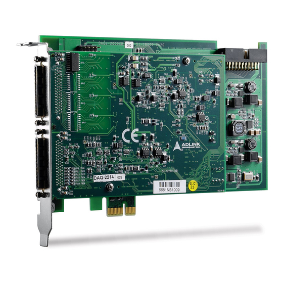
Page 30: Card Layout
2.3 Card Layout DAQe-2204/2205/2206/2208 Figure 2-1: DAQe-2204/2205/2206/2208 Card Layout Installation Artisan Technology Group - Quality Instrumentation ... Guaranteed | (888) 88-SOURCE | www.artisantg.com... -
Page 31: Daq-2204/2205/2206/2208
DAQ-2204/2205/2206/2208 Figure 2-2: DAQ-2204/2205/2206/2208 Card Layout PXI-2204/2205/2206/2208 Figure 2-3: PXI-2204/2205/2206/2208 Card Layout Installation Artisan Technology Group - Quality Instrumentation ... Guaranteed | (888) 88-SOURCE | www.artisantg.com... -
Page 32: Pci Configuration
2.4 PCI Configuration Plug and Play With support for plug and play, the card requests an interrupt num- ber via its PCI controller. The system BIOS responds with an inter- rupt assignment based on the card information and on known system parameters. - Page 33 Installation Artisan Technology Group - Quality Instrumentation ... Guaranteed | (888) 88-SOURCE | www.artisantg.com...
-
Page 34: Signal Connections
Signal Connections This chapter describes DAQ-/DAQe-/PXI-2204/2205/2206/2208 card connectors and the signal connection between the DAQ-/ DAQe-/PXI-2204/2205/2206/2208 card and external devices. 3.1 Connectors Pin Assignment The DAQ-/DAQe-/PXI-2204/2205/2206/2208 card is equipped with two 68-pin VHDCI-type connector (AMP-787254-1). It is used for digital input/output, analog input/output, timer/counter signals, etc. -
Page 35: Cn1 Connector
CN1 Connector AI0 (AIH0) (AIL0) AI32 AI1 (AIH1) (AIL1) AI33 AI2 (AIH2) (AIL2) AI34 AI3 (AIH3) (AIL3) AI35 AI4 (AIH4) (AIL4) AI36 AI5 (AIH5) (AIL5) AI37 AI6 (AIH6) (AIL6) AI38 AI7 (AIH7) (AIL7) AI39 AI8 (AIH8) (AIL8) AI40 AI9 (AIH9) 10 (AIL9) AI41 AI10 (AIH10) (AIL10) AI42... -
Page 36: Table 3-2: Cn1 Pin Assignment For Daq-/Daqe-/Pxi-2208
AI0 (AIH0) (AIL0) AI48 AI1 (AIH1) (AIL1) AI49 AI2 (AIH2) (AIL2) AI50 AI3 (AIH3) (AIL3) AI51 AI4 (AIH4) (AIL4) AI52 AI5 (AIH5) (AIL5) AI53 AI6 (AIH6) (AIL6) AI54 AI7 (AIH7) (AIL7) AI55 AISENSE AIGND AI8 (AIH8) 10 (AIL8) AI56 AI9 (AIH9) (AIL9) AI57 AI10 (AIH10) 12 (AIL10) AI58... -
Page 37: Cn2 Connector
CN2 Connector DA0OUT AOGND DA1OUT AOGND AOEXTREF AOGND DGND DGND EXTWFTRIG DGND EXTDTRIG DGND SSHOUT SDI0 / DGND* RESERVED SDI1 / DGND* RESERVED 10 SDI2 / DGND* AFI1 SDI3 / DGND* AFI0 12 DGND GPTC0_SRC 13 DGND GPTC0_GATE 14 DGND GPTC0_UPDOWN 15 DGND GPTC0_OUT 16... -
Page 38: Table 3-4: Cn2 Pin Assignment Fordaq-/Daqe-/Pxi-2208
AI32 (AIH32) (AIL32) AI80 AI33 (AIH33) (AIL33) AI81 AI34 (AIH34) (AIL34) AI82 AI35 (AIH35) (AIL35) AI83 AI36 (AIH36) (AIL36) AI84 AI37 (AIH37) (AIL37) AI85 AI38 (AIH38) (AIL38) AI86 AI39 (AIH39) (AIL39) AI87 EXTATRIG AIGND AI40 (AIH40) 10 (AIL40) AI88 AI41 (AIH41) (AIL41) AI89 AI42 (AIH42) 12 (AIL42) AI90... -
Page 39: Table 3-5: Cn1/Cn2 Signal Description
CN1/CN2 Connector Signal Description Signal Name Reference Direction Description Analog ground for AI. All three ground references (AIGND, AIGND — — AOGND, and DGND) are connected together on board. • For DAQ-/DAQe-/PXI-2204/ 2205/2206: Analog Input Channels 0~63. Each channel pair, AI<i, i+32> (I=0..31) can be configured either two single- ended inputs or one differential input pair(marked as... - Page 40 Signal Name Reference Direction Description Synchronous digital inputs. These SDI<0..3> 4 digital inputs are sampled DGND Input (for 2204 only) simultaneously with the analog signal input. GPTC<0,1>_SRC DGND Input Source of GPTC<0,1> GPTC<0,1>_GATE DGND Input Gate of GPTC<0,1> GPTC<0,1>_OUT DGND Input Output of GPTC<0,1>...
-
Page 41: Ssi Connector
SSI Connector SSI_TIMEBASE DGND SSI_ADCONV DGND SSI_DAWR / RESERVED* DGND SSI_SCAN_START DGND RESERVED DGND SSI_AD_TRIG DGND SSI_DA_TRIG / RESERVED* DGND RESERVED DGND RESERVED DGND RESERVED DGND Table 3-6: SSI Connector Pin Assignment *Pin 5 and 13 are reserved for DAQ/PXI-2208. SSI Connector Signal Description: SSI Timing Signal Setting Function... -
Page 42: Analog Input Signal Connection
3.2 Analog Input Signal Connection The DAQ-/DAQe-/PXI-2204/2205/2206/2208 card provides up to 64 single-ended or 32 differential analog input channels. You can fill the Channel Gain Queue to get desired combination of the input signal types. The analog signal can be converted to digital values by the A/D converter. -
Page 43: Figure 3-1: Floating Source And Rse Input Connections
Referenced Single-ended (RSE) Mode In referenced single-ended mode, all input signals are con- nected to the ground provided by the DAQ-/DAQe-/PXI-2204/ 2205/2206/2208 card. This is suitable for connections with floating signal sources. Figure 3-1 shows an illustration. Note that when more than two floating sources are connected, these sources will be referenced to the same common ground. -
Page 44: Differential Input Mode
Differential Input Mode The differential input mode provides two inputs that respond to signal voltage difference between them. If the signal source is ground-referenced, the differential mode can be used for the com- mon-mode noise rejection. Figure 3-3 shows the connection of ground-referenced signal sources under differential input mode. - Page 45 Signal Connections Artisan Technology Group - Quality Instrumentation ... Guaranteed | (888) 88-SOURCE | www.artisantg.com...
-
Page 46: Operation Theory
Operation Theory The operation theory of the DAQ-/DAQe-/PXI-2204/2205/2206/ 2208 card functions are described in this chapter. The functions include the A/D conversion, D/A conversion, digital I/O, and gen- eral purpose counter/timer. The operation theory can help you understand how to configure and program the DAQ-/DAQe-/PXI- 2204/2205/2206/2208 card. -
Page 47: Figure 4-1: Synchronous Digital Inputs Block Diagram
SDI<3..0> SDI<3..0> 16-bit from CN2 Register From Data AD<11..0> Instrumentation FIFO Amplifier nADBUSY nADBUSY AD_conversion nADCONV Figure 4-1: Synchronous Digital Inputs Block Diagram AD_conversion nADBUSY 16 bits data(including AD<11..0> and SDI<3..0> latched into AD Data FIFO Figure 4-2: Synchronous Digital Inputs Timing NOTE Since the analog signal is sampled when an A/D conver- sion starts (falling edge of A/D_conversion signal), while... -
Page 48: Table 4-1: Bipolar Analog Input Range And Output Digital Code On Daq/Daqe/Pxi-2204/2208
Table 4-1and Table 4-2 illustrate the ideal transfer characteristics of various input ranges of the DAQ-/DAQe-/PXI-2204/2205/2206/ 2208 card. Digital Description Bipolar Analog Input Range code Full-scale Range ±10V ±5V ±2.5V ±1.25V — Least significant bit 4.88mV 2.44mV 1.22mV 0.61mV — FSR-1LSB 9.9951V 4.9976V... -
Page 49: Daq/Daqe/Pxi-2005/2006/2016 Ai Data Format
DAQ/DAQe/PXI-2005/2006/2016 AI Data Format The data format of the acquired 16-bit A/D data is 2's Comple- ment coding. Table 4-3 and Table 4-4 illustrate the valid input ranges and the ideal transfer characteristics. Digital Description Bipolar Analog Input Range code Full-scale Range ±10V ±5V... -
Page 50: Software Conversion With Polling Data Transfer
Software Conversion with Polling Data Transfer Acquisi- tion Mode (Software Polling) This is the easiest way to acquire a single A/D data. The A/D con- verter starts one conversion whenever the dedicated software command is executed. Then the software would poll the conver- sion status and read the A/D data back when it is available. -
Page 51: Programmable Scan Acquisition Mode
Programmable Scan Acquisition Mode Scan Timing and Procedure It is recommended that you use this mode if your applications need a fixed and precise A/D sampling rate. You can accu- rately program the period between conversions of individual channels. There are at least four counters which need to be specified: SI_counter (24-bit): Specify the Scan Interval = SI_counter / Timebase... -
Page 52: Figure 4-3: Scan Timing
3 Scans, 4 Samples per scan (PSC_Counter=3, NumChan_Counter=4) ( channel sequences are specified in Channel Gain Queue) Scan_start AD_conversion Scan_in_progress (SSHOUT)(pin8 on CN2) Acquisition_in_progress Sampling Interval t= Scan Interval T= SI2_COUNTER/TimeBase SI_COUNTER/TimeBase Figure 4-3: Scan Timing There are four trigger modes to start the scan acquisition. Refer to section 4.1 for details. -
Page 53: Specifying Channels, Gains, And Input Configurations In The Channel Gain Queue
Scan with SSH You can send the SSHOUT signal on CN2 to external S&H cir- cuits to sample and hold all signals if you want to simulta- neously sample all channels in a scan, as illustrated in Figure 4-3. NOTES The DAQ-/DAQe-/PXI-2208 does not support this func- tion. - Page 54 Then Acquisition sequence of channels: 1, 2, 0, 2, 1, 2, 0, 2, 1, 2, 0, 2 Sampling interval: 160/40 Ms = 4 µs Scan interval: 640/40 Ms = 16 µs Equivalent sampling rate of ch0, ch1: 62.5 kHz Equivalent sampling rate of ch2: 125 kHz Operation Theory Artisan Technology Group - Quality Instrumentation ...
-
Page 55: Trigger Modes
Trigger Modes The DAQ-/DAQe-/PXI-2204/2205/2206/2208 card provides four trigger sources (internal software trigger, external analog trigger, and digital trigger sources, and SSI trigger signals). You must select one of them as the source of the trigger event. A trigger event occurs when the specified condition is detected on the selected trigger source. -
Page 56: Figure 4-4: Pre-Trigger (Trigger Occurs After M Scans)
Pre-Trigger Acquisition Use pre-trigger acquisition in applications where you want to collect data before a trigger event. The A/D starts to sample when you execute the specified function calls to begin the pre- trigger operation, and it stops when the trigger event occurs. Users must program the value M in M_counter (16 bits) to specify the amount of the stored scans before the trigger event. -
Page 57: Figure 4-5: Pre-Trigger (Trigger With Scan In Progress)
Note that if a trigger event occurs when a scan is in progress, the data acquisition won't stop until the scan completes, and the stored M scans of data includes the last scan. Therefore, the first stored data will always be the first channel entry of a scan (that is, the first channel entry in the Channel Gain Queue if the number of entries in the Channel Gain Queue is equivalent to the value of NumChan_counter), no matter when a trigger signal occurs, as... -
Page 58: Figure 4-6: Pre-Trigger With M_Enable=0 (Trigger Occurs Before M Scans)
When the trigger signal occurs before the first M scans of data are converted, the amount of stored data could be fewer than the orig- inally specified amount M_counter, as illustrated in Figure 4-6. This situation can be avoided by setting M_enable. If M_enable is set to 1, the trigger signal will be ignored until the first M scans of data are converted, and it assures the user M scans of data under pre-trigger mode, as illustrated in Figure 4-7. -
Page 59: Figure 4-7: Pre-Trigger With M_Enable=1
(M_counter = M = 3, NumChan_counter=4, PSC_counter=0) The first M scans Trigger signals which occur in the shadow region(the first M scans) will be ignored Trigger Scan_start AD_conversion Scan_in_progress (SSHOUT)(pin2 on CN2) Acquisition_in_progress Aquired data Acquired & stored data (M scans) Operation start Figure 4-7: Pre-trigger with M_enable=1 NOTE... -
Page 60: Figure 4-8: Middle-Trigger With M_Enable = 1
Middle-Trigger Acquisition Use middle-trigger acquisition in applications where you want to collect data before and after a trigger event. The number of scans (M) stored before the trigger is specified in M_counter, while the number of scans (N) after the trigger is specified in PSC_counter. -
Page 61: Figure 4-9: Middle-Trigger (Trigger Occurs When A Scan Is In Progress)
If the trigger event occurs when a scan is in progress, the stored N scans of data would include this scan, as illustrated in Figure 4-9. Figure 4-9: Middle-Trigger (Trigger occurs when a scan is in progress) Operation Theory Artisan Technology Group - Quality Instrumentation ... Guaranteed | (888) 88-SOURCE | www.artisantg.com... -
Page 62: Figure 4-10: Post-Trigger
Post-Trigger Acquisition Use post-trigger acquisition in applications where you want to collect data after a trigger event. The number of scans after the trigger is specified in PSC_counter, as illustrated in Figure 4- 10. The total acquired data length = NumChan_counter * PSC_counter. -
Page 63: Figure 4-11: Delay Trigger
Delay Trigger Acquisition Use delay trigger acquisition in applications where you want to delay the data collection after the occurrence of a specified trig- ger event. The delay time is controlled by the value, which is pre-loaded in the Delay_counter (16-bit). The counter counts down on the rising edge of the Delay_counter clock source after the trigger condition is met. -
Page 64: Figure 4-12: Post Trigger With Re-Trigger
Post-Trigger or Delay-trigger Acquisition with re-trigger Use post-trigger or delay-trigger acquisition with re-trigger function in applications where you want to collect data after several trigger events. The number of scans after each trigger is specified in PSC_counter, and users could program Retrig_no to specify the re-trigger numbers. -
Page 65: Bus-Mastering Dma Data Transfer
Bus-mastering DMA Data Transfer PCI bus-mastering DMA is necessary for high speed DAQ in order to utilize the maximum PCI bandwidth. The bus-mastering control- ler, which is built in the PLX IOP-480 PCI controller, controls the PCI bus when it becomes the master of the bus. Bus mastering reduces the size of the on-board memory and reduces the CPU loading because data is directly transferred to the computer’s memory without host CPU intervention. -
Page 66: Figure 4-13: Scatter/Gather Dma For Data Transfer
Figure 4-13 shows a linked list that is constructed by three DMA descriptors. Each descriptor contains a PCI address, a local address, a transfer size, and the pointer to the next descriptor. You can allocate many small size memory blocks and chain their associative DMA descriptors altogether by their application pro- grams. -
Page 67: D/A Conversion
4.2 D/A Conversion NOTE The DAQ-/DAQe-/PXI-2208 card does not support this function. There are two 12-bit D/A output channels available in the DAQ-/ DAQe-/PXI-2204/2205/2206 card. When using D/A converters, you should assign and control the D/A converter reference sources for the D/A operation mode and D/A channels. You could also set the output polarity to unipolar or bipolar. -
Page 68: Software Update
Digital Code Analog Output 111111111111 Vref * (4095/4096) 100000000000 Vref * (2048/4096) 000000000001 Vref * (1/4096) 000000000000 Table 4-6: Unipolar Output Code Table The D/A conversion is initiated by a trigger source. You must decide how to trigger the D/A conversion. The data output will start when a trigger condition is met. -
Page 69: Timed Waveform Generation
Timed Waveform Generation This mode can provide your applications with a precise D/A output with a fixed update rate. It can be used to generate an infinite or finite waveform. You can accurately program the update period of the D/A converters. The D/A output timing is provided through a combination of counters in the FPGA on board. -
Page 70: Figure 4-14: Typical D/A Timing Of Waveform Generation
4 update counts, 3 iterations (UC _Counter=4, IC_Counter=3) Trigger UC_Counter=4 DAWR WFG_in_progress Delay until Delay until Delay until DLY1_Counter DLY2_Counter DLY2_Counter reaches 0 reaches 0 reaches 0 DA update_interval t= UI_Counter/Timebase Output Waveform Operation start A single waveform IC_Counter = 3 Figure 4-14: Typical D/A Timing of Waveform Generation NOTE The maximum D/A update rate is 1 MHz. -
Page 71: Trigger Modes
Trigger Modes Post-Trigger Generation Use post-trigger when you want to perform DA waveform right after a trigger event occurs. In this trigger mode DLY1_Counter is ignored and not be specified. Figure 4-15 shows a single waveform generated right after a trigger signal is detected and assuming the data in the data buffer are 2V, 4V, 6V, 3V, 0V, - 4V, -2V, and 4V. -
Page 72: Figure 4-16: Delay Trigger Waveform Generation
Figure 4-16: Delay Trigger Waveform Generation Post-Trigger or Delay-Trigger with Re-trigger Use post-trigger or delay-trigger with re-trigger function when you want to generate waveform after more than one trigger events. The re-trigger function can be enabled or disabled by software setting. In Figure 4-17, each trigger signal will initiate a waveform generation assuming the data in the data buffer are 2V, 4V, 2V, and 0V. -
Page 73: Figure 4-18: Finite Iterative Waveform Generation With
Iterative Waveform Generation Set IC_Counter in order to generate iterative waveforms from the data of a single waveform. The counter stores the iteration number and the iterations may be finite (Figure 4-18) or infinite (Figure 4-19). Take note that in infinite mode the waveform generation does not stop until software stop function is exe- cuted and IC_Counter is still valid when stop mode III is selected. -
Page 74: Figure 4-19: Infinite Iterative Waveform Generation With
Figure 4-19: Infinite Iterative Waveform Generation with Post-trigger (DLY2_Counter = 0) Delay2 in Iterative Waveform Generation To stretch out the flexibility of the D/A waveform generation, we add a DLY2_Counter to separate two consecutive waveforms in iterative waveform generation. The time between two wave- forms is assigned by setting the value of the DLY2_Counter. -
Page 75: Figure 4-20: Stop Mode I
Stop Modes of Scan Update You can call software stop function to stop waveform genera- tion when it is still in progress. Three stop modes are provided for timed waveform generation meant to stop the waveform generation. You can apply these three modes to stop wave- form generation no matter infinite or finite waveform generation mode is selected. -
Page 76: Figure 4-21: Stop Mode Ii
In stop mode II, after a software stop command is given, the waveform generation does not stop until a complete single waveform is finished. See Figure 4-21. Since the UC_counter is set to four, the total DA update counts (number of pulses of DAWR signal) must be a multiple of four (update counts = 20 in this example). -
Page 77: Digital I/O
4.3 Digital I/O The DAQ-/DAQe-/PXI-2204/2205/2206/2208 card contains 24 lines of general-purpose digital I/O (GPIO) which is provided through the 82C55A chip. The 24-line GPIO are separated into three ports: Port A, Port B and Port C. High nibble (bit[7…4]), and low nibble (bit[3…0]) of each port can be programmed individually to be either inputs or outputs. -
Page 78: The Basics Of Timer/Counter Functions
The Basics of Timer/Counter Functions Each timer/counter has three inputs that can be controlled via hardware or software. These are clock input (GPTC_CLK), gate input (GPTC_GATE), up/down control input (GPTC_UPDOWN). The GPTC_CLK input provides a clock source input to the timer/counter. Active edges on the GPTC_CLK input make counter... -
Page 79: Figure 4-23: Mode1 Operation
Mode1: Simple Gated-Event Counting In this mode, the counter counts the number of pulses on the GPTC_CLK after the software-start. Initial count can be loaded from software. Current count value can be read-back by soft- ware any time without affecting the counting. GPTC_GATE is used to enable/disable counting. -
Page 80: Figure 4-24: Mode2 Operation
Figure 4-24: Mode2 Operation Mode3: Single Pulse-width Measurement In this mode, the counter counts the pulse-width of the signal on GPTC_GATE in terms of GPTC_CLK. Initial count can be loaded from software. After the software-start, the counter counts the number of active edges on GPTC_CLK when GPTC_GATE is in its active state. -
Page 81: Figure 4-26: Mode4 Operation
Mode4: Single Gated Pulse Generation This mode generates a single pulse with programmable delay and programmable pulse-width following the software-start. The two programmable parameters could be specified in terms of periods of the GPTC_CLK input by software. GPTC_GATE is used to enable/disable counting. When GPTC_GATE is inac- tive, the counter halts the current count value. -
Page 82: Figure 4-27: Mode5 Operation
Figure 4-27: Mode5 Operation Mode6: Re-triggered Single Pulse Generation This mode is similar to Mode5 except that the counter gener- ates a pulse following every active edge of GPTC_GATE. After the software-start, every active GPTC_GATE edge triggers a single pulse with programmable delay and pulse-width. Any GPTC_GATE triggers that occur when the prior pulse is not completed would be ignored. -
Page 83: Figure 4-29: Mode7 Operation
Mode7: Single Triggered Continuous Pulse Generation This mode is similar to Mode5 except that the counter gener- ates continuous periodic pulses with programmable pulse inter- val and pulse-width following the first active edge of GPTC_GATE. Once the first GPTC_GATE edge triggers the counter, GPTC_GATE takes no effect until the software-start is re-executed. -
Page 84: Trigger Sources
4.5 Trigger Sources ADLINK provides flexible trigger selections in the DAQ-/DAQe-/ PXI-2204/2205/2206/2208 card. In addition to the internal soft- ware trigger, the DAQ-/DAQe-/PXI-2204/2205/2206/2208 card also supports external analog, digital triggers, and SSI triggers. You can configure the trigger source by software for A/D and D/A processes individually. -
Page 85: Table 4-7: Analog Trigger Src1 (Extatrig) Ideal Transfer Characteristic
Figure 4-31: Analog Trigger Block Diagram Trigger level digital setting Trigger voltage 0xFF 9.92V 0xFE 9.84V 0x81 0.08V 0x80 0x7F -0.08V 0x01 -9.92V Table 4-7: Analog Trigger SRC1 (EXTATRIG) Ideal Transfer Characteristic The trigger signal is generated when the analog trigger condition is satisfied. -
Page 86: Figure 4-32: Below-Low Analog Trigger Condition
Below-Low Analog Trigger Condition Figure 4-32 shows the below-low analog trigger condition, the trigger signal is generated when the input analog signal is less than the Low_Threshold voltage, and the High_Threshold set- ting is not used in this trigger condition. Figure 4-32: Below-Low Analog Trigger Condition Above-High Analog Trigger Condition Figure 4-33 shows the above-high analog trigger condition, the... -
Page 87: Figure 4-34: Inside-Region Analog Trigger Condition
Inside-Region Analog Trigger Condition Figure 4-34 shows the inside-region analog trigger condition, the trigger signal is generated when the input analog signal level falls in the range between the High_Threshold and the Low_Threshold voltages. NOTE The High_Threshold setting should be always higher than the Low_Threshold voltage setting. -
Page 88: Figure 4-35: High-Hysteresis Analog Trigger Condition
Figure 4-35: High-Hysteresis Analog Trigger Condition Low-Hysteresis Analog Trigger Condition Figure 4-36 shows the low-hysteresis analog trigger condition, the trigger signal is generated when the input analog signal level is less than the Low_Threshold voltage, and the High_Threshold voltage determines the hysteresis duration. Note the High_Threshold setting should be always higher then the Low_Threshold voltage setting. -
Page 89: Figure 4-37: External Digital Trigger
External Digital Trigger An external digital trigger occurs when a rising edge or a falling edge is detected on the digital signal connected to the EXT- DTRIG or the EXTWFTRG of the 68-pin connector for external digital trigger. The EXTDTRIG is dedicated for A/D process, and the EXTWFTRG is used for D/A process. -
Page 90: User-Controllable Timing Signals
4.6 User-controllable Timing Signals In order to meet the requirements for user-specific timing and requirements for synchronizing multiple cards, the DAQ-/DAQe-/ PXI-2204/2205/2206/2208 card provides flexible user-controllable timing signals to connect to external circuitry or additional cards. The whole DAQ timing of the DAQ-/DAQe-/PXI-2204/2205/2206/ 2208 card is composed of a bunch of counters and trigger signals in the FPGA. -
Page 91: Daq Timing Signals
You can utilize the flexible timing signals through our software drivers, then simply and correctly connect the signals with the DAQ-/DAQe-/PXI-2204/2205/2206/2208 card. Here is the sum- mary of the DAQ timing signals and the corresponding functional- ities for DAQ-/DAQe-/PXI-2204/2205/2206/2208 card. Timing signal category Corresponding functionality SSI/PXI signals... - Page 92 width of the TIMEBASE to guarantee correct functional- ities. 4. ADCONV, the conversion signal to initiate a single con- version, which could be derived from internal counter, AFI[0] or SSI_ADCONV. Note that this signal is edge- sensitive. When using AFI[0] as the external ADCONV source, each rising edge of AFI[0] would bring an effec- tive conversion signal.
-
Page 93: Auxiliary Function Inputs (Afi)
Auxiliary Function Inputs (AFI) You can use the AFI in applications that take advantage of exter- nal circuitry to directly control the DAQ-/DAQe-/PXI-2204/2205/ 2206/2208 card. The AFI includes two categories of timing signals: one group is the dedicated input, and the other is the multi-func- tion input. - Page 94 intervals for both A/D and D/A operations. Note that once you choose the TIMEBASE source, both A/D and D/A operations will be affected because A/D and D/A operations share the same TIMEBASE. AFI[0] Alternatively, you can also directly apply an external A/D con- version signal to replace the internal ADCONV signal.
-
Page 95: System Synchronization Interface
System Synchronization Interface SSI (System Synchronization Interface) provides the DAQ timing synchronization between multiple cards. In DAQ-/DAQe-/PXI- 2204/2205/2206/2208 card, we designed a bi-directional SSI I/O to provide flexible connection between cards and allow one SSI master to output the signal and up to three slaves to receive the SSI signal. - Page 96 In PXI form factor, we utilize the PXI trigger bus built on the PXI backplane to provide the necessary timing signal connections. All the SSI signals are routed to the P2 connector. No additional cable is needed. For detailed information of the PXI specifications, refer to the PXI Specification Revision 2.0 from PXI System Alliance (www.pxisa.org).
- Page 97 The SSI/PXI Mechanism We adopt master-slave configuration for SSI/PXI. In a system, for each timing signal, there shall be only one master, and other cards are SSI slaves or with SSI function disabled. For each timing signal, the SSI master does not have to be in a single card.
-
Page 98: Calibration
Calibration This chapter introduces the calibration process to minimize AD measurement errors and DA output errors. 5.1 Loading Calibration Constants The DAQ-/DAQe-/PXI-2204/2205/2206/2208 card is factory-cali- brated before shipment. The associated calibration constants of the TrimDACs firmware to the onboard EEPROM. TrimDACs are devices containing multiple DACs within a single package. -
Page 99: Auto-Calibration
5.2 Auto-calibration Through the DAQ-/DAQe-/PXI-2204/2205/2206/2208 card auto- calibration feature, the calibration software measures and corrects almost all calibration errors without any external signal connec- tions, reference voltage, or measurement devices. The DAQ-/DAQe-/PXI-2204/2205/2206/2208 card comes with an onboard calibration reference to ensure the accuracy of auto-cali- bration. -
Page 100: Warranty Policy
Warranty Policy Thank you for choosing ADLINK. To understand your rights and enjoy all the after-sales services we offer, please read the follow- ing carefully. 1. Before using ADLINK’s products please read the user man- ual and follow the instructions exactly. When sending in damaged products for repair, please attach an RMA appli- cation form which can be downloaded from: http:// rma.adlinktech.com/policy/. - Page 101 3. Our repair service is not covered by ADLINK's guarantee in the following situations: Damage caused by not following instructions in the User's Manual. Damage caused by carelessness on the user's part dur- ing product transportation. Damage caused by fire, earthquakes, floods, lightening, pollution, other acts of God, and/or incorrect usage of voltage transformers.
- Page 102 Artisan Technology Group is your source for quality new and certified-used/pre-owned equipment SERVICE CENTER REPAIRS WE BUY USED EQUIPMENT • FAST SHIPPING AND DELIVERY Experienced engineers and technicians on staff Sell your excess, underutilized, and idle used equipment at our full-service, in-house repair center We also offer credit for buy-backs and trade-ins •...
Need help?
Do you have a question about the DAQe Series and is the answer not in the manual?
Questions and answers