Table of Contents
Advertisement
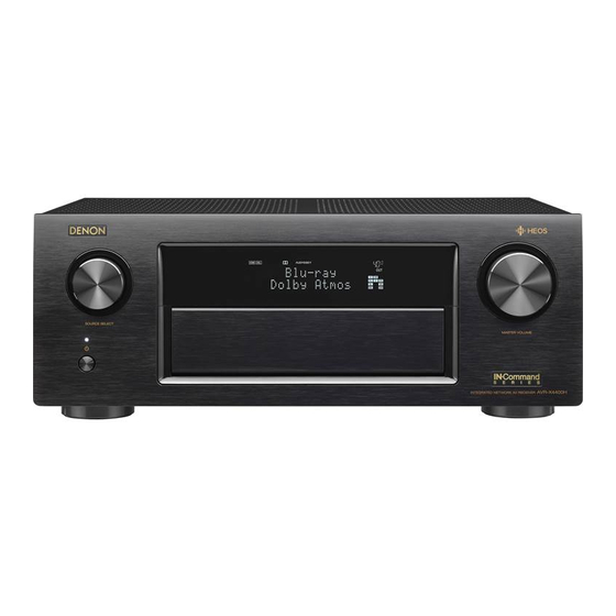
INTEGRATED NETWORK AV RECEIVER
AVR-X4400H
• For purposes of improvement, specifications and design are subject to change without notice.
• Please use this service manual with referring to the operating instructions without fail.
• Some illustrations using in this service manual are slightly different from the actual set.
Service Manual
Click here!
On-line service parts list
http://dmedia.dmglobal.com/Document/DocumentDetails/23507
Online Parts List
(P5 to P7)
WEB owner's manual
http://manuals.denon.com/AVRX4400H/NA/EN/index.php (July 2017)
http://manuals.denon.com/AVRX4400H/EU/EN/index.php (July 2017)
http://manuals.denon.com/AVRX4400H/AP/ZH/index.php (September 2017)
CAUTION IN SERVICING
ELECTRICAL
MECHANICAL
REPAIR INFORMATION
UPDATING
Ver. 1
(Release schedule)
Advertisement
Table of Contents

Related Manuals for Denon AVR-X4400H


Summary of Contents for Denon AVR-X4400H
- Page 1 INTEGRATED NETWORK AV RECEIVER Click here! AVR-X4400H On-line service parts list http://dmedia.dmglobal.com/Document/DocumentDetails/23507 Online Parts List (P5 to P7) WEB owner’s manual (Release schedule) http://manuals.denon.com/AVRX4400H/NA/EN/index.php (July 2017) http://manuals.denon.com/AVRX4400H/EU/EN/index.php (July 2017) http://manuals.denon.com/AVRX4400H/AP/ZH/index.php (September 2017) CAUTION IN SERVICING ELECTRICAL MECHANICAL REPAIR INFORMATION UPDATING • For purposes of improvement, specifications and design are subject to change without notice.
-
Page 2: Caution In Servicing
CAUTION IN SERVICING SAFETY PRECAUTIONS NOTE FOR SCHEMATIC DIAGRAM NOTE FOR PARTS LIST INSTRUCTIONS FOR HANDLING SEMICONDUCTORS AND OPTICAL UNIT Online Parts List Accessing the Parts List Logging in to New SDI and Accessing the Parts List Accessing the Part List from the Model Asset Screen PRINTED CIRCUIT BOARDS Parts Table Downloading the Parts List as an Excel File Revision History... -
Page 3: Safety Precautions
SAFETY PRECAUTIONS ◎ Make a safety check after servicing! The following items should be checked for continued protection of the customer and the service Check that all screws, parts and wires removed or disconnected when servicing have been put back technician. -
Page 4: Note For Schematic Diagram
NOTE FOR SCHEMATIC DIAGRAM WARNING: Parts indicated by the z mark have critical characteristics. Use ONLY replacement parts recommended by the manufacturer. CAUTION: Before returning the set to the customer, be sure to carry out either (1) a leakage current check or (2) a line to chassis resistance check. - Page 5 Online Parts List Accessing the Parts List Logging in to New SDI and Accessing the Parts List (1) Click the URL link on the cover of the service manual. (1) Access New SDI from the URL below. Examples of display <http://dmedia.dmglobal.com>...
-
Page 6: Revision History
Accessing the Part List from the Model Asset Screen Downloading the Parts List as an Excel File (1) Display Model Asset from New SDI. (1) Displays the Parts List. Click the Download icon. (2) Click the section displayed as ▼ Link to Part Lists under the model name. NOTE : If the ▼... - Page 7 Searching Part Numbers or Ref. Numbers You can search a Parts List for part numbers or Ref. numbers. (1) Enter the part number or Ref. number in the search window of the Parts List, and press the search button. (2) The search results are displayed. The name of the sheet in which the search part is used and the part’s line are displayed.
-
Page 8: Initializing This Unit
CAUTION IN SERVICING. Initializing This Unit Make sure to initialize this unit after replacing the microcomputer or any peripheral equipment, or the digital PCB. 1. Press the power button to turn off the power. 2. While holding down buttons "CURSOR d " and "CURSOR f " simultaneously, press the power button to turn on the power. -
Page 9: Schematic Diagrams
ELECTRICAL SCHEMATIC DIAGRAMS BLOCK DIAGRAM SCH35_FRONT SCH36_SMPS SCH01_DIGITAL CONNECT ANALOG AUDIO DIAGRAM SCH02_DIGITAL POWER DIGITAL AUDIO DIAGRAM PRINTED CIRCUIT BOARDS SCH03_MAIN CPU VIDEO DIAGRAM SCH04_EXPANDER HDMI DIAGRAM DIGITAL SCH05_CPU LEVEL CHG INPUT, USB, F-HDMI POWER DIAGRAM SCH06_DIR VIDEO, GUIDE, SIDE CNT, FRONT CONT FFC SCH07_AUDIO PLD SPK, SPK H2L, GUIDE TRANS, GUIDE TOP, GUIDE SIDE SCH08_DSP1... - Page 10 SCHEMATIC DIAGRAMS SCH01_DIGITAL CONNECT TO 4B TO DIGITAL SUPPLY (PAGE 2_B1) DAC input CH1: DATAF BN27A BN27A CH2: DACLRCK L1001 CJP15HJ282Z C125Z2-15 R1021 0.1uF L1051 600 ohm CPUPOWER R1022 0.01uF CH3: DACBCK L1052 600 ohm M3.3V R1023 1000pF BN24A L1053 600 ohm DGND C1051...
- Page 11 SCH02_DIGITAL POWER PJ02 PJ01 CN903 L1221 BLM21PG221SN1 L1222 DGND D5.2V BLM21PG221SN1 C1235, C1237 L1223 D5.2V BLM21PG221SN1 M_RESET DV1.8V AVRX4400H OPEN TO BN901 DGND 1.34A R1111 DV_POWER2 DGND IC111 L1113 L1111 TPS563200DDCR MAINPOWER CB03YTYH600 C1236, C1238 CB03YTYH600 L1224 CB03YTYH600 L1112 L1115 L1114 AVRX4400H OPEN...
- Page 12 SCH03_MAIN CPU TO 2D TO 3D TO B7 TO B3 TO A7 TO B1 TO B2 TO LEVEL CHG. TO DIGITAL CNT (PAGE 5) (PAGE 1) R1577 4.7K DA_MS DA_CK R1578 OPEN R1579 OPEN DA_MD R1581 OPEN DSP_ICS DSP_ICS DSP_MOSI DSP_MOSI DSP_MISO DSP_MISO...
- Page 13 SCH04_EXPANDER TO 2E TO 3E TO 4E TO 5E TO A4 TO B0 TO A6 TO DIGITAL CNT TO VIDEO PLD TO HDMI TX TO HDMI SW1 TO HDMI SW2 (PAGE 16_C6) PAGE 1 (PAGE 13_A4) (PAGE 17_D6) (PAGE 14_A3) R1702 4.7K SWM3.3V...
- Page 14 SCH05_CPU LEVEL CHG TO D2 TO A8 TO C8 TO DIGITAL CONNECT TO MAIN CPU (PAGE 1_A4) (PAGE 3_D5) TO DIGITAL SUPPLY POWER (PAGE 2_B1) T206 T186 T185 3.3K R1967 2SC3052 2SC3052 2SC3052 Q1907 Q1910 Q1913 Q1922 Q1923 T246 Q1902 T247 T187 T188...
- Page 15 Z2DIRDATA MPIO DIRAUXMCK 2.2K DIRAUXMCK Z2DIRLRCK COAX OUT C2011 LRCKO DIRSLRCK R2024 DIRSLRCK Z2DIRBCK DIRSBCK 1/10V Z2DIRMCK DIRSBCK DEMZ2 (DENON LINK HD) BCKO DIRPERR Q2002 DIRPERR DIRNPCM DIRNPCM JK204 MCKO TO 9E CJJ4M073ZY IC203 RJ-0111R-29T KRC107S LC89091JA-H HDMISPDIF HDMISPDIF DENONLINKHD...
- Page 16 SCH07_AUDIO PLD MCU_VL_MUTE MCU_VL_MUTE VOL_MUTE VOL_MUTE TO D5 TO MAIN CPU JTAG_TMS PLDAERR1 PLDAERR1 JTAG_TDI Z2PLDAERR (PAGE 3_C1) Z2PLDAERR TO E8 JTAG_TCK Z3PLDAERR R2249 Z3PLDAERR TDO1_TDI2 IC222 SPDIF_OUT SPDIF_OUT OPEN MCLK_I2S_0 C2203 MCLK_I2S_0 LRCK_I2S_0 TO E6 LRCK_I2S_0 APLD_CS TO LEVEL CHG SDIN_I2S_0 SDIN_I2S_0 AVRX4400H...
- Page 17 SCH08_DSP1 TO F6 TO 3G TO F7 TO 4G TO 5G TO 6G TO 7G TO D4 TO A.PLD PART TO MAIN CPU PART TO DSP2 PART TO DSP4 PART TO DSP3 PART TO DSP2 PART TOAUDIO PLD TO DSP2 PART (PAGE 7_A5) (PAGE 8-2_D5) (PAGE 7_A5)
- Page 18 SCH09_DSP2 TO G3 TO G4 TO 9G TO G7 TO F8 TO DSP1 PART TO DSP3 PART TO DSP1 PART TO A.PLD TO DSP1 PART (PAGE 8-3_D3) (PAGE 8-1_D2) (PAGE 7_A4) (PAGE 8-1_D4) (PAGE 8-1_D3) D3I_FW D3I_CSW D3I_FH D3I_SB D3I_RSV D3I_F D3I_S IC262...
- Page 19 SCH10_DSP3 TO F5 TO 1H TO F9 TO G9 TO G6 TO DSP2 PART TO ADUDIO PLD PART TO DSP1 PART TO DSP4 PART TO AUDIO PLD (PAGE 8-4_D5) (PAGE 7_A4) (PAGE 8-2_D3) (PAGE 8-1_D2) (PAGE 7_A5) IC272 C2745 1000P A3V56S40GTP-60 256M BIT SDRAM C2737...
- Page 20 SCH11_DSP4 TO H1 TO G0 TO G5 TO ADUDIO PLD PART TO DSP3 PART TO DSP1 PART (PAGE 8-3_D4) (PAGE 7_A3) (PAGE 8-1_D2) IC282 C2855 1000P A3V56S40GTP-60 256M BIT SDRAM C2847 VDD_INT DAI_P09 C2856 0.1 R2845 DSP4_FLAG0 FLAG0 DAI_P05 R2846 4.7K C2857 0.1 DQ15...
- Page 21 SCH12_ADC TO G1 TO D1 (PAGE 7_A3) (PAGE 3_C6) (PAGE 6_C5) TO AUDIO PLD TO MAIN CPU TO DIR A+5V AD_VDCOM ADINL ADINR DAGND C3055 C3056 TO B5 C3057 1000P C3058 1000P C3061 1000P C3062 1000P C3063 1000P C3064 1000P C3066 1000P C3067 1000P C3068 1000P...
- Page 22 SCH13_ZONE, LEGO DAC TO G2 (PAGE 7_A2) TO AUDIO PLD IC324 BU33TD3WG VIN VOUT ZONE_DAC STBY ZONE2 DAC IC321 PCM5100APWR DVDD CPVDD C3201 C3203 DGND CAPP C3202 2.2/6.3V LDOO CPGND XSMT CAPM VNEG Z2DACMUTE LRCK OUTL R3203 Z2DACLRCK DAZONE2L OUTR R3204 Z2DACDATA DAZONE2R...
- Page 23 SCH14_LEGO FROM LEGO MODULE CN502 CN501 CJP80GA370ZU CJP42GA370ZU LEGO5V DGND BK106 BK107 BK108 BK109 ST501 VMD1A960 VMD1A960 VMD1A960 VMD1A960 NET3.3V L5002 TO B8 C5011 OPEN 600 ohm VOUT_D22 VOUT_D23 IC521 VOUT_D20 OPEN VOUT_D21 VOUT_D18 VOUT_D19 VOUT_D16 VOUT_D17 C5012 VOUT_D14 R5507 VOUT_D15 OPEN VOUT_D12...
- Page 24 SCH15_VIDEO DECODER DVDDIO_3.3V L3551 DV3.3V BLM21PG221SN1 DV1.8V DGND DVDD_1.8V L3561 DV5V BLM21PG221SN1 TO C0 PVDD_1.8V L3571 22uH/0.32A/2518 AVDD_1.8V L3581 22uH/0.32A/2518 D3542 KDS160 X3501 R3549 R3550 C3501 Q3543 28.636MHz KRC102S Q3541 4.7K R3541 KTA1504SYRTK 7180_DO Q3542 R3502 C3502 C3543 KRC105S KEEP CLOSE WITH ADV7180 R3510 &...
- Page 25 SCH16_HDMI SW2 CEC5V CEC3.3V L3801 VDD33 BLM21PG221SN1 Q3841 CEC1.1V-2 HDMI_SW2 TO C4 Q3842 DGND KRC102S HPD1 L3802 HPD1 AVDD33TX RX1_C- BLM21PG221SN1 R3845 KRC102S RX1_5V RX1_C+ +5V_1 19.HP DET RX1_0- 18.+5V RX1_0+ 17.GND RX1_1- C3860 L3809 16.DDC DATA R3847 RX1_1+ RX1_DDCDA AVDD33RX CLZBLM21PG300SN1D R3848...
- Page 26 SCH17_HDMI SW1 Z2_CEC5V CEC5V HDMI_SW2 TO C3 P2_C- CEC3.3V L3901 P2_C+ VDD33 BLM21PG221SN1 P2_D0- CEC1.1V-1 P2_D0+ P2_D1- DGND P2_C- P2_C- P2_D1+ L3902 P2_C+ P2_D2- P2_C+ AVDD33TX BLM21PG221SN1 P2_D0- P2_D2+ P2_D0- P2_D0+ P2_D0+ P2_D1- RX5_C- P2_D1- P2_D1+ P2_D1+ RX5_C+ P2_D2- RX5_0- P2_D2- L3910 P2_D2+...
- Page 27 SCH18_VSP & IP & OSD TO DIGITAL POWER SUPPLY (PAGE 2_B3) TO C1 L4001 CB03YTYH600 L4002 CB03YTYH600 L4003 L4008 L4013 CB03YTYH600 CB03YTYH600 CB03YTYH600 L4004 L4010 CB03YTYH600 CB03YTYH600 L4016 CB03YTYH600 L4012 L4005 CB03YTYH600 L4014 CB03YTYH600 CB03YTYH600 IC403 IC402 A3R12E40DBF-8E L4006 A3R12E40DBF-8E 512Mbit DDR2 SDRAM L4015 CB03YTYH600...
- Page 28 SCH19_VIDEO PLD TO C2 TO F3 TO DIGITAL POWER TO AUDIO PLD (PAGE 2_B3) (PAGE 7_D1) MCU&LEGO ADV8003 VPLD_TRANS2 VPLD_TRANS2 PO8KI_C9/G1_PLD PO8KI_C9/G1 VPLD_TRANS1 VPLD_TRANS1 TO EXPANDER RN429 VPLD_TRANS0 PO8KI_Y0/G4_PLD PO8KI_Y0/G4 VPLD_TRANS0 33x4 PO8KI_Y11/R7_PLD PO8KI_Y11/R7 N_PCK (PAGE 4_C4) TTL_SEL_A ADV7180 TTL_SEL_A PO8KI_Y3/G7_PLD 8KOPI_HSYNC IO-001...
- Page 29 SCH20_HDMI TX & ARC TO C5 CEC5V CEC3.3V AVDD11TX CEC1.1V-3 VDD33 C4403 OPEN L4305 L4308 BLM21PG221SN1 VDD11 BLM21PG221SN1 DGND L4301 C4402 OPEN TP102 BLM21PG221SN1 C4401 OPEN JK432 C4400 OPEN A0D7ABAR1990 C4396 HDMI_OUT L4321 PTX0_2+ 1.D2+ L4310 AVDD11RX L4309 AVDD33RX C4409 OPEN PTX0_2- 2.D2 SHIELD...
- Page 30 SCH21_INPUT BN64C BN24C BN23C TO CN64C TO CN24C TO CN23C FROM SIDE CONNECT PART FROM FRONT CONNECT PART FROM SIDE CONNECT PART (PAEG 27_B2) (PAEG 24_B2) (PAEG 27_B4) BN64C BN24C BN23C C125Z2-13 C125Z2-27 C125Z2-21 R4843 100K R4761 100K R4772 100K BN461 R4739 R4762...
- Page 31 SCH22_PREOUT PREOUT PART C8992 R8849 C8849 0.1uF 10/50V C8993 0.1uF D8845 1N4007 C8996 0.1uF C8913 R8913 R8915 C8917 R8921 D8846 1N4007 R8846 PREZ2L C8994 0.01uF BN26C C8991 D8847 1N4007 22/50V 22/50V C8995 0.01uF P_PRESW1MUTE R8925 R8927 C8997 0.01uF 0.1uF P_PRECMUTE OPEN P_PRESMUTE ADCINL...
- Page 32 SCH23_F-HDMI Q1001 Q1002 KRA102S R1002 KRC103S JK101 A0D7ABAR19N0 C1001 R1003 T103 19.HP DET 18.+5V T102 CN101 CEC5V 17.GND L1001 16.DDC DATA T104 60R/3A 15.DDC CLK T105 CN101 14.NC 13.CEC CJP23GA333ZR 12.CK- 11.D1 SHIELD CEC3.3V L1002 DDCD_SDA 10.CK+ DDCD_SCL 9.D0- 60R/3A TXEN 8.D1 SHIELD HPA_D...
- Page 33 SCH24_A-VIDEO VIDEO+5V TO 5J VGND VIDEO-5V ANALOG VDIEO PART IC513 NJM2845DL133 +3.3V LEGO_FAN_POWER TO 6J LEGO_FAN_GND LEGO_FAN_ON CVBS IN/OUT JK511 C5107 CBL/SAT SAT_CVBS_IN 50V/10uF C5108 DVD_CVBS_IN 50V/10uF R5183 DEC_CVBS_IN C5109 R5184 GAME GAME_CVBS_IN DEC_Y_IN 50V/10uF R5185 DEC_PB_IN R5186 MONITOR DEC_PR_IN R5187 75(1%) MON_COMP_CR_OUT...
- Page 34 SCH25_RC-5 RC-5 OPEN R5311 BN27B R5312 Q5313 BN27B KRA102S Q5311 L5311 60R/3A(BEAD) KRA102S M3.3V L5312 60R/3A(BEAD) Q5312 DGND L5313 60R/3A(BEAD) KRC102S RC_IN L5314 60R/3A(BEAD) KILLIR RC_OUT FRONT_IRIN L5315 60R/3A(BEAD) FLASHER_IN Q5314 REMOTE3.3V 232O_MI KRA102S 232I_MO TRIGGER_1 TRIGGER_2 JK531 B/P_IRIN_AVR R5314 D5311 OPEN Q5315 TO CN27B...
- Page 35 SCH26_RS232C_TRIGGER IR / FLASHER RS232C/TRIGGER IC521 ILX3232DT C5237 C5236 50V/0.1uF 50V/10uF C5231 C5235 C5245 50V/0.01uF 50V/0.1uF 50V/0.1uF C5246 50V/0.1uF C5247 OPEN D5231 JK525 OPEN T1_O R5234 RS-232C R1_I R5233 Q5251 D5232 KRA102S C5233 R1_O OPEN 50V/0.1uF Q5252 2SC3052 C5234 T1_I C5241 50V/0.1uF C5244 50V/0.01uF JK521...
- Page 36 TU_TXMI/SDA FROM/TO RC-5/MX-PORT PART TU_GND PAGE 20_A5 CN961 TO BN961 12511HS-13 CN27C OPEN J9631 CN28C OPEN J9633 CN28C C125Z1-07 CN27C C125Z1-15 AVR-X4400H CN28B CN27B J9632 J9661 J9632 CN27B CN28B C125Z1-07 C125Z1-15 CN27B X4400H CN28B J9662 X4400H TO BN27B TO BN28B...
- Page 37 SCH28_FRT CNT CN21A CN25A CN26A CN24A TO BN21A TO BN25A TO BN26A TO BN24A FROM/TO DIGITAL CON. PART FROM/TO DIGITAL CON. PART PAGE 1_B3 FROM/TO DIGITAL CON. PART FROM/TO DIGITAL CON. PART PAGE 1_D3 PAGE 1_D5 PAGE 1_B5 FRT CNT CONNECT B CN26A CN21A CN25A...
- Page 38 SCH29_MAIN DAC1 A+5V C3055 0.1uF A-7V C3056 0.1uF 1000pF A+7V C3057 C3058 1000pF DAGND C3059 OPEN C3060 OPEN C3061 1000pF 1000pF C3062 C3063 1000pF R3017 C3064 0.1uF R3021 4.7K C3065 0.1uF C3066 0.1uF R3013 C3017 R3027 R3025 C3067 1000pF 3.9K 680pF C3068 1000pF...
- Page 39 SCH30_MAIN DAC2 A+5V C3147 0.1uF A-7V C3148 0.1uF 1000pF C3149 A+7V C3150 1000pF DAGND C3151 OPEN C3152 OPEN C3153 0.1uF R3125 C3154 0.1uF C3155 1000pF R3123 4.7K C3156 1000pF ASSIGNR1 C3125 R3127 R3113 3.9K R3121 680pF R3119 R3111 3.9K (GRM21) C3130 (GRM21) 470uF...
- Page 40 SCH31_SPK R9211 2W/10 JK921 BN701 C9211 BN701 L9201 0.047uF(M) 0.01uF(M) C9531 C9511 OPEN +HIGHB 0.5uH R9201 JW934A JW931A JK922 1W/10 TO CN701 R9212 JW929A JW927A JW927B JW926A HIGH_GND R9202 2W/10 C9532 0.01uF(M) C9512 OPEN JW933A JW932A 1W/10 C9212 F_RLY L9202 0.5uH 0.047uF(M) C9224...
- Page 41 SCH32_REGULATOR CN711 20010WS-03 Q9402 CJP03GI352ZY 2SA2166 MAX 130mA R9400 FAN1_OUT 0(3216) R9401 FAN PART OPEN FAN1_GND Q9406 KTC3964 Q9404 FAN2_OUT Q9403 KRA107S KRC105S FAN2_GND FANCONT_ON1 CN712 20010WS-03 CJP03GI352ZY Q9405 FANCONT_L_ON1 KRC105S TO K3 Q9412 MAX 130mA R9410 2SA2166 0(3216) R9411 OPEN Q9416 KTC3964...
- Page 42 SCH33_5CH AMP Point C1 R7116 R7117 D7102 OPEN 63.7V R7138 R7115 R7118 1.2K(1608) 1.2K(1608) R7119 PTC 115'C 470 ohm D7101 OPEN 1W/270 CN715 1W/270 OPEN Q7114 R7137 62.9V Q7138 D7118 MMBT5401 58.5V 680K(1608) MMBT5401 C7111 1SS133M C7108 Q7118 R7143 1.1V R7129 D7139 R7139...
- Page 43 SCH34_4CH AMP R7616 R7617 D7602 OPEN R7615 R7618 R7638 1.2K(1608) 1.2K(1608) R7619 D7601 OPEN 1W/270 1W/270 CN765 PTC 115'C 470 ohm OPEN R7637 Q7614 Q7638 MMBT5401 D7618 MMBT5401 1SS133M 680K(1608) C7611 C7608 Q7800 Q7618 R7629 R7643 OPEN D7639 R7639 MMBT5401 KTA1024Y 1W/22 Q7631...
- Page 44 SCH35_FRONT CN69A TO CN69B FROM DIGITAL CONNECT (PAGE 1_B1) LUG61 OPEN FIL1 R6003 VOLUME ENCODER PART FIL1 R6004 OPEN SWM3.3V FIL2 SWM3.3V FIP POWER PART OPEN VSELA VSELA R6352 R6354 DGND 4.7K C6904 OPEN VSELB OPEN FIL2 R6005 C6905 OPEN FRONT_IRIN AC37V C6906...
- Page 45 SCH36_SMPS SMPS PART OPTION AC100 ~ 120V CCQF2E104KZE-T AC220 ~ 240V OPEN BK901 OPTION CMD1A834 AC100 ~ 120V : T 2A L 250V C9002 OPTION OPTION AC220 ~ 240V : T 1.6A L 250V OPTION CHGND 0.01uF/250V J9008 F9001 1N4007 D9001 JK901 C3A206...
-
Page 46: Lead-Free Solder
PRINTED CIRCUIT BOARDS DIGITAL Lead-free Solder When soldering, use the Lead-free Solder (Sn-Ag-Cu). DIGITAL (A SIDE) D4332 D4312 D3962 D3804 R3844 D4317 R3848 C2007 Z2_DA R3847 R3843 T192 Z2_HPD D3803 Z2_+5V T191 D2001 JK432 D4338 M2_HPD JK431 D3967 D3945 HPD6 HPD5 HPD4 HPD3... - Page 47 INPUT, USB, F-HDMI INPUT (A SIDE) INPUT (B SIDE) F_HDMI(B SIDE) F_HDMI(A SIDE) BK101 CUP12867Z_MP T114 T117 C1027 T116 T118 C1023 T115 L1002 C1015 C1012 C1013 R1008 R1007 BAR CODE LABEL USB (A SIDE) USB (B SIDE)
- Page 48 4.VIDEO-5V 5.VIDEO-5V R5232 R5231 J9662 LEGO_FAN ON J9631 J9632 VGND VGND 6.TRG_GND C5234 CN28B C5328 7.TRG+12V D5321 C5233 R5233 C5231 AVR-X4400H CN27B 232O_MI CN27B R5326 J9661 AVR-X4400H 232I_MO J9632 R5327 R5234 J9610 CN28B J9611 R5325 REMOTE_+3.3V J9623 J9662 C5163 C5232...
- Page 49 SPK, SPK H2L, GUIDE TRANS, GUIDE TOP, GUIDE SIDE SPK (A SIDE) SPK H2L (A SIDE) SPK H2L (A SIDE) CN951 JK930 CUP12920Z_A-2 MP C9539 J9252 J9253 JK924 C9534 JK929 JK923 JW930A JK928 J9254 JK931 C9541 J9204 JK926 C9536 C9537 JK925 C9535 C9533...
- Page 50 5CH AMP, 4CH AMP 5CH AMP (A SIDE) 5CH AMP (B SIDE) 4CH AMP (A SIDE) 4CH AMP (B SIDE) D7402 D7401 C7423 R7415 R7417 R7416 R7435 Q7439 C7419 D7419 R7735 D7702 R7715 R7135 C7723 R7136 D7102 R7115 R7717 R7716 C7123 C7719 D7719...
- Page 51 FRONT, HDMI FFC TOP FRONT (A SIDE) HDMI FFC TOP (A SIDE) JW605 C6027 C6082 C6035 BK606 C6008 BK603 JW604 LUG61 FRONT HDMI FL601 CN69A JW603 CN602 CN602 7.VKK 7.VKK C6025 J6012 FFC CABLE B'D 6.NC 6.NC 5.VKK GND 5.VKK GND 4.NC 4.NC 3.FIL2...
- Page 52 FRONT CNT, TUNER, BKT, SMPS FRONT CNT (A SIDE) FRONT CNT (B SIDE) SMPS (A SIDE) SMPS (B SIDE) Sec. Sec. Sec. Sec. Pri. Pri. Pri. Pri. Pri. Pri. Sec. Sec. Pri. Pri. Sec. Sec. C9008 C9007 Q9003 D9010 R9037 C9006 R9043 R9035...
-
Page 53: Level Diagram
LEVEL DIAGRAM FRONT ch AVR-X4400H LEVEL DIAGRAM FRONT ch NJU72343 NJU72750 ANALOG H/POUT NJU72750 NJU72750 SPEAKER LINE + GAIN ADJ. - AK4458 MIC IN + + + AK5358 - - MUTE PRE OUT TO ZONE2 x4pcs TO ZONE3 +30dB 4.24Vrms/8Ω... - Page 54 CENTER / SURROUND ch AVR-X4400H LEVEL DIAGRAM CENTER/SURROUND ch NJU72343 SPEAKER + GAIN ADJ. AK4458 + + - - MUTE PRE OUT x4pcs +30dB 4.24Vrms/8Ω Volume IC: NJU72343 NON CLIP MAX SIGNAL LEVEL 4.2Vrms SPK OUT DAC:AK4458 1.98Vrms=0dBFS FULL SCALE LEVEL = 2.0Vrms...
- Page 55 SUBWOOFER ch AVR-X4400H LEVEL DIAGRAM SUB WOOFER ch NJU72343 GAIN ADJ. AK4458 + + - - MUTE PRE OUT x4pcs +30dB +30dB FULL SCALE LEVEL Volume IC: NJU72343 NON CLIP MAX SIGNAL LEVEL 4.2Vrms DOLBY LIMIT LEVEL (ALL ch -3dBFS)
- Page 56 ASSIGN1 / 2 (SURR.BACK / HEIGHT1 / HEIGHT2) ch AVR-X4400H LEVEL DIAGRAM ASSIGN1/2 (SURROUND BACK/HEIGHT1/HEIGHT2) ch NJU72343 NJU72750 SPEAKER + GAIN ADJ. AK4458 + + - - MUTE PRE OUT x4pcs +30dB 4.24Vrms/8Ω Volume IC: NJU72343 NON CLIP MAX SIGNAL LEVEL 4.2Vrms...
- Page 57 ZONE2 / ZONE3 ch AVR-X4400H LEVEL DIAGRAM ZONE2/ZONE3 NJU72750 LINE To MAIN MUTE PRE OUT NJU72750 MONO PCM5100 NJW1194V MONO Z2 DAC NJU72750 MONO NJW1194V + SPEAKER PCM5100 Z3 DAC MONO MUTE PRE OUT +30dB NJW1194V MAX. OUTPUT 4.2Vrms SP OUT 4.24Vrms/8Ω...
- Page 58 BLOCK DIAGRAM ANALOG AUDIO DIAGRAM AVRX4400H ANALOG AUDIO BLOCK NJU72750AV MAIN_L RY871 PREFL 11.2ch Processing DAFL PREFR ADCL NJU72343V PREC Z2FL ADZ2L PREC PREFL PRESW1 DALEGOZ2L PREFR PRESL MAIN_R PREFL PREC DAFR PRESR PRESW1 PREFR PREASS1L ADCR Z2FR DAASSIGN2L PREASS2L PRESL PREASS1R ADZ2R...
- Page 59 DIGITAL AUDIO DIAGRAM AVRX4400H DIGITAL AUDIO BLOCK(ADI) DIRRST #146 DIRCE #143 DIRDIN #141 DIRDOUT #144 Z3DIRSPDIF DIGTAL IN DIRCLK #145 Z2DIRSPDIF 24.576MHz COAX0 PLDADCDATA DATAAD ADINL MAIN COAX1 ZONE3 ZONE2 COAX0 DIRADLRCK PLDADCLRCK OPT1(TV) OPT0 PLDADCSBCK DIRADBCK ADINR COAX1 OPT1 AK5358BET (To MAIN DIR) SPDIF_OUT...
- Page 60 VIDEO DIAGRAM AVRX4400H ANALOG VIDEO BLOCK AVDM2000 CBL/SAT CBL/SAT_V VOUT5 DVD_V CVBS IN GAME GAME_V VOUT4 DEC_CVBS_IN Z1 MONITOR Z1 CVBS V.AUX(FRONT) V.AUX_V DVD_V CBL/SAT_V Z2 MONITOR Z2 CVBS GAME_V VOUT3 Z2 MONITOR V.AUX_V MONITOR VOUT2 COMPONENT OUT Y COMPONENT OUT PB VOUT1 COMPONENT OUT PR Blu-ray_Y...
- Page 61 HDMI DIAGRAM AVRX4400H/SR7012/AV7704/SR6012 HDMI BLOCK HDMI SW2(MN864788) HDMI ZONE2 P3 RX HDMI IN1 (CBL/SAT) MAIN P0 TX P2 RX HDMI IN2 HDMI TX(MN864787) (DVD) P1 RX P1 RX P1 TX HDMI IN3 (BLU-RAY) P0 RX P0 RX HDMI Rx 600MHz 600MHz 4K/2K HDMI IN4...
-
Page 62: Power Diagram
POWER DIAGRAM AVRX4400H POWER BLOCK DIAGRAM HI+B LOW+B 426.5mA RY931 +12V(RELAY) (389mA) S1(AMP+B,-B) SPK Relay(5EA)+ Small Relay(0EA)+H/L Relay(1EA)+Fan(2EA) 221 + 12.5 + 33 + 160 = 426.5mA LOW-B HI-B 96mA +3.3V (Z2, Z3, LEGO DAC) BU33TD3WG (55mA) 32+32+32=96mA (191.5mA) IC323 333mA 283mA 187mA... -
Page 63: Wiring Diagram
WIRING DIAGRAM WIRING DIAGRAM (AVRX4400H) WiFi Antenna WiFi Antenna HEIGHT PCB PCB DIGITAL PCB CUP12920Z-2 WiFi Antenna WiFi Antenna CN951 CUP12916Z WAFER/3P/2.5mm CJP03GI289ZY CN321 CON1 CON2 WAFER/5P/2mm CJP05GI288ZY BN951 LEGO MODULE INLET WIRE/3P/2.5mm/50mm VWB1E0030503D CN781 CN704 (CNVLEGOAIOS4025) WAFER/6P/2mm WAFER/7P/2mm (PROT.LINE) (PROT.LINE) CN431 CJP06GA208ZY... - Page 64 SEMICONDUCTORS Only major semiconductors are shown, general semiconductors etc. are omitted to list. The semiconductor which described a detailed drawing in a schematic diagram are omitted to list. 1. IC's R5F564MJCDFC (DIGITAL : IC151) Pin Name Symbol Pu/Pd STBY STOP Function STBY E20 Emulator control pin (On chip Emulator is used,this...
- Page 65 Pin Name Symbol Pu/Pd STBY STOP Function Pin Name Symbol Pu/Pd STBY STOP Function STBY STBY NC(X4400)/ P80/SCK10 DSP_CLK DSP(ADI) control pin DA3VPu KILL_ PC4/SCK5 DSP1FLAG0 DSP(ADI) interrupt signal input pin P24/SCK3 IR(SR6012/ Front IR disable control pin PC3/TXD5 DSP2FLAG0 DSP(ADI) interrupt signal input pin SR7012/ P77/TXD11...
- Page 66 Pin Name Symbol Pu/Pd STBY STOP Function Pin Name Symbol Pu/Pd STBY STOP Function STBY STBY ASO/DC_ Power supply pin DET(X4400/ P47/IRQ15-DS/ Protection detect signal input pin (for ASO and DC) (A/ ARC_INT ARC IC interrupt signal input pin PE7/IRQ7/AN105 SR6012/ AN007 D converter) SR7012) /...
- Page 67 PCM9211 www.ti.com SBAS495 – JUNE 2010 AD8195 PIN CONFIGURATIONS AD8195ACPZ (F-HDMI : IC101) PCM9211 (DIGITAL : IC202) PT PACKAGE LQFP-48 PIN CONFIGURATION AND FUNCTION DESCRIPTIONS (TOP VIEW) ERROR/INT0 VDDRX 30 AVCC PIN 1 30 AVCC NPCM/INT1 RXIN1 29 PE_EN INDICATOR PIN 1 29 PE_EN INDICATOR...
- Page 68 PCM9211 PCM9211 BLOCK DIAGRAM www.ti.com SBAS495 – JUNE 2010 BLOCK DIAGRAM DESCRIPTION NAME FILT TOLERANT AUXIN 0 26 MS/ADR1 Software control I/F, SPI chip select / I2C slave address AUTO RXIN7 setting1(2) RXIN 0 RXIN0 SCKO DOUT RXIN 1 RXIN1 MAIN OUTPUT 27 MODE...
- Page 69 A3V56S40GTP 256M Single Data Rate Synchronous DRAM ADSP21487KSWZ4B (DIGITAL : IC251 / IC261 / IC271 / IC281) A3V56S40GTP-60 (DIGITAL : IC252 / IC262 / IC272 / IC282) Pin Configuration (Top View) PIN 1 PIN CONFIGURATION (TOP VIEW) GND PAD DQ15 (PIN 177) DQ14 DQ13...
-
Page 70: Pin Function
AK4458VN 40 +105 C (Exposed pad is connected to ground) 40 +85 C (Exposed pad is open) 48-pin QFN (0.5mm pitch) AKD4458 Evaluation Board for AK4458 AK4458VN (FRONT CNT : IC301, IC311) No. Pin Name I/O Function PD State CAD0_I2C Chip Address 0 Pin in I2C Bus serial control mode Pin Configurations Chip Select Pin in 3-wire serial control mode... - Page 71 SLAS764 – MAY 2011 www.ti.com [AK4458] DEVICE INFORMATION TERMINAL FUNCTIONS, PCM510x FUNCTIONAL BLOCK DIAGRAM PCM5100 (DIGITAL IC321, IC322, IC323) 4. Block Diagram and Functions PCM510X (top view) LDOE TVDD VDD18 DVSS AVDD AVSS Bias BICK/DCLK DATT AOUTL1P LRCK/DSDL1 Soft Mute Interpolator AOUTL1N SDTI1/DSDR1...
- Page 72 G Bipolar Technology G Package Outline DIP16,DMP16 GENERAL DESCRIPTION PACKAGE OUTLINE The NJM2586A is a wide band 3-input 1-output 3-circuit video I PIN CONFIGURATION and BLOCK DIAGRAM NJU72343 (INPUT : IC471, IC491) NJM2595MTE1 ( amplifier. It is suitable for Y, Pb, and Pr signal because frequency IC511) VIDEO : range is 50MHz.The NJM2586A is suitable for AV receiver, STB,...
- Page 73 PATTERN DETAIL ANODE CONNECTION 2. FL DISPLAY 1G-16G 1G-16G 1G-16G FLD (17-BT-40GINK) (FRONT : FL601) 1-1A 1-1B 2-1A 2-1B 3-1A 3-1B 4-1A 4-1B 5-1A 5-1B 1-2A 1-2B 2-2A 2-2B 3-2A 3-2B 4-2A 4-2B 5-2A 5-2B D10A 1-3A D10B 1-3B D11A 2-3A D11B 2-3B...
- Page 74 3. Remote Code Table FORMAT SHARP FORMAT: SHARP / DATA CONSTRUCTION 15bits C14 0 C15 0=NOT INVERTED, 1=INVERTED /REMOTE ID : 1 FORMAT: SHARP / DATA CONSTRUCTION 15bits C14 0 C15 0=NOT INVERTED, 1=INVERTED /REMOTE ID : 1 SYSTEM ADDRESS(C1~C5) : 00110 , EXTENSION BIT (C12,C13) : 01 SYSTEM ADDRESS(C1~C5) : 01000...
- Page 75 FORMAT: SHARP / DATA CONSTRUCTION 15bits C14 0 C15 0=NOT INVERTED, 1=INVERTED /REMOTE ID : 1 FORMAT: SHARP / DATA CONSTRUCTION 15bits C14 0 C15 0=NOT INVERTED, 1=INVERTED /REMOTE ID : 1 SYSTEM ADDRESS(C1~C5) : 00110 , EXTENSION BIT (C12,C13) : 10 SYSTEM ADDRESS (C1~C5) : 01000...
- Page 76 / DATA CONSTRUCTION 15bits C14 0 C15 0=NOT INVERTED, 1=INVERTED /REMOTE ID : 1 FORMAT KASEIKYO DATA CONSTRUCTION 48bits SYSTEM ADDRESS (C1~C5) : 00100 , EXTENSION BIT (C12,C13) : 01 DENON CODE Parity GENRE1(*1) Data (C6~C11) Data (C6~C11) Key Name...
- Page 77 RCKSK0410030 CURSOR RIGHT RCKSK0410429 RHL LEVEL UP RCKSK0410031 ENTER RCKSK0410430 RHL LEVEL DOWN RCKSK0410034 RETURN/BACK RCKSK0410431 RHR LEVEL UP RCKSK0410035 SETUP MENU RCKSK0410432 RHR LEVEL DOWN RCKSK0410036 MEMORY RCKSK0410433 FDL LEVEL UP RCKSK0410434 FDL LEVEL DOWN RCKSK0410042 UPGRADE ID ON RCKSK0410435 FDR LEVEL UP RCKSK0410045...
- Page 78 RCKSK0410765 Pandora (NA only) ZONE2 RCKSK0410787 INPUT SOURCE SELECT Right RCKSK0410788 INPUT SOURCE SELECT Left REMOTE ID SET: 1 RCKSK0410789 Graphic EQ (toggle) DENON CODE Parity GENRE1 GENRE2 RCKSK0410791 Graphic EQ ON 4 5 2 3 0 RCKSK0410792 Graphic EQ OFF...
- Page 79 RCKSK0450716 RCKSK0450718 ZONE3 USB RCKSK0450719 ZONE3 FM TUNER ZONE3 RCKSK0450720 ZONE3 DVD RCKSK0450721 ZONE3 Blu-ray REMOTE ID SET: 1 RCKSK0450722 ZONE3 TV AUDIO DENON CODE Parity GENRE1 GENRE2 RCKSK0450723 ZONE3 CBL/SAT 4 5 2 3 0 RCKSK0450725 ZONE3 GAME 25 26 27 28...
- Page 80 ANALOG TUNER HEOS MUSIC REMOTE ID SET: 1 REMOTE ID SET: 1 DENON CODE Parity GENRE1 GENRE2 DENON CODE Parity GENRE1 GENRE2 4 5 2 3 0 25 26 27 28 4 5 2 3 0 9 10 11 12 13 14 15 16...
- Page 81 MECHANICAL DISASSEMBLY Flowchart 1. WiFi ANT 2. FRONT ASSY 3. RADIATOR ASSY 4. REAR PANEL 5. DIGITAL PCB 6. VIDEO PCB 7. INPUT PCB 8. TUNER PCB 9. SPK PCB 10. SMPS PCB 11. TRANS EXPLODED VIEW PACKING VIEW...
- Page 82 DISASSEMBLY Flowchart • Remove each part following the flow below. • Reassemble the removed parts in the reverse order. • Read "SAFETY PRECAUTIONS" before reassembling the removed parts. • If wire bundles are removed or moved during adjustment or part replacement, reshape the wires after completing the work. Failure to shape the wires correctly may cause problems such as noise. •...
-
Page 83: Front Assy
• The photographs with no shooting direction indicated were taken from the top of the unit. (1) Remove the screws. • Photos of AVR-X4400H E3 are used in this manual. The viewpoint of each photograph (Shooting direction : X) [View from the top] ↓Shooting direction: B↓... - Page 84 (3) Remove the connector. 3. RADIATOR ASSY Proceeding : TOP COVER → FRONT ASSY → RADIATOR ASSY (1) Remove the screws. View from the bottom ↑Shooting direction: A↑ (2) Cut the wire clamp, then remove the connector. 4. REAR PANEL CN462 Proceeding : TOP COVER...
-
Page 85: Digital Pcb
5. DIGITAL PCB 6. VIDEO PCB Proceeding : TOP COVER → WiFi ANT → REAR PANEL → DIGITAL PCB Proceeding : TOP COVER → WiFi ANT → REAR PANEL → DIGITAL PCB → VIDEO PCB (1) Remove the screws. Remove the Rivet. Cut the wire clamp, then remove the connector. (1) Remove the connector. -
Page 86: Tuner Pcb
8. TUNER PCB Proceeding : TOP COVER → WiFi ANT → REAR PANEL → DIGITAL PCB → VIDEO PCB → INPUT PCB → TUNER PCB "EXPLODED VIEW" for instructions on removing the TUNER PCB. 9. SPK PCB Proceeding : TOP COVER →... -
Page 87: Exploded View
EXPLODED VIEW http://dmedia.dmglobal.com/Document/DocumentDetails/23507 Parts List : EXPLODED VIEW [AVRX4400H] S10 x10 S8 x4 S9 x4 S9 x3 S2 x5 S4 x5 M12 x5 S4 x4 S5 X15 S5 X12 S4 x4 M12 x5 S4 x5 S4 x2 S2 x5 S12 x4 S2 x2 C49 X11 S13 x3... -
Page 88: Packing View
PACKING VIEW http://dmedia.dmglobal.com/Document/DocumentDetails/23507 Parts List : UK plug (UK Only) 'H' TAPING 'I' TAPING [AVRX4400HBKE3/AVRX4400HBKE2/AVRX4400HSPE2] 18-1 CONTROL LABEL [AVRX4400HBKE1C] [AVRX4400HK] 18-3 18-2 18-4 18-1 18-1 18-2 CONTROL LABEL CONTROL LABEL... -
Page 89: Troubleshooting
REPAIR INFORMATION TROUBLE SHOOTING SPECIAL MODE 1. POWER Special mode setting button 2. Analog video 1. Version Display Mode 3. HDMI/DVI 2. PANEL / REMOTE LOCK Selection Mode 4. AUDIO 3-1. Selecting the Mode for Service-related 5. Network / Bluetooth / USB 3-2. - Page 90 TROUBLE SHOOTING 1. POWER 1.1. The unit does not power on The unit does not power on Disconnect the connector [CN903] that supplies power from the Measure the voltage of the DIGITAL PCB [CN903 : 5, 6pin]. SMPS PCB to the DIGITAL PCB and measure the voltage of the SMPS Is the fuse blown out? "6.
-
Page 91: Analog Video
2. Analog video Perform the operation below beforehand. b Check it whether connection cable and Monitor are normal. b VIDEO Convert is set to ON. Input b Setting as follows. CVBS / COMPONENT V : SAT COMPONENT : SAT Is the power voltage being output correctly? MONITOR OUT (CVBS / COMPONENT / HDMI OUT NG SIDE CNT PCB ·... - Page 92 DIGITAL test point D4332 D4312 D3962 D3804 R3844 D4317 R3848 C2007 Z2_DA R3847 R3843 T192 Z2_HPD D3803 Z2_+5V T191 JK432 D4338 M2_HPD JK431 D4319 D3967 D3945 HPD6 HPD5 HPD4 HPD3 HPD2 HPD1 D3802 T190 D2001 D4343 D4342 D4339 TP39 D4323 D3946 HPD7 D3852...
- Page 93 3.1. No picture or sound is output (HDMI to HDMI) No picture or sound is output. (8) When using a DENON Blu-ray/DVD player, is the "HDMI" indicator of the fluorescent display lit? Proceed to YES when using a Blu-ray/DVD player produced by other manufactures.
- Page 94 (15) Are a picture and sound output when a differ- The TV is faulty. ent TV is used? Check the unit. "HDMI "Rx/Tx" Failure Detection"...
- Page 95 4. AUDIO 4.1. AUDIO CHECK No audio output CHECK 1 INPUT SURROUND MODE SOURCE Check the ANALOG AUDIO BLOCK Audio output OK? ANALOG 2CH DIRECT ANALOG CHECK 2 INPUT SURROUND MODE SOURCE Check the DIGITAL AUDIO BLOCK Legacy Audio output OK? COAX or OPT (PCM or DolbyDigital or dts…) CHECK 3...
-
Page 96: Analog Audio
4.2. Power AMP (AMP PCB) 4.3. Analog audio When using the protection pass mode, do not connect speakers to the speaker terminals. No audio output. No audio output. Protection is activated. Is a voltage of ± 8V supplied to INPUT PCB Repair the ±... -
Page 97: Cannot Connect To The Network
5. Network / Bluetooth / USB 5.1. Cannot connect to the network Check the connection environment The circuit of NET5V POWER Insert the LAN cable correctly and then turn on Can the output voltage (5V) to Is NET5V POWER [IC151 : 48pin Is the LAN cable correctly inserted? between [IC151-Q1101 : FET- the power again. - Page 98 5.2. Cannot establish a Bluetooth connection Check the Bluetooth device being used Are the versions of the HEOS Version displayed in The Network Module software is faulty. Version Check Mode? Is the Bluetooth device compatible with the A2DP Use a device that is A2DP profile compatible. profile? The circuit of Network Module is faulty.
- Page 99 5.3. Cannot recognize the connected USB device 5.4. No picture or sound is output Check the USB device being used Checking the unit (If no picture is output) Are digital video signals(LEGOPCK, LEGOVS, The circuit around Network Module, [IC421 : V.PLD] Is a USB hub being used? Do not use a USB hub.
- Page 100 DIGITAL test point USB test point D4332 D4312 D3962 D3804 R3844 JK608 D4317 Z2_DA R3848 C2007 R3847 R3843 T192 Z2_HPD D3803 Z2_+5V JK432 D4338 M2_HPD JK431 HPD5 HPD4 HPD3 D3802 T191 T190 D2001 TP39 D4319 D3967 D3946 D3945 HPD6 HPD2 HPD1 D4343 D4342...
- Page 101 6. SMPS Operation waveform for each part DC 5V is not output. After primary side rectification Primary drain (Caution: High voltage, electric shock) After secondary rectifications (Caution: High voltage, electric shock) Replace the [IC901 : TOP268EG Is [IC901 : TOP268EG] damaged? and D9001 / D9002 / D9003 / C9002 OPTION...
- Page 102 HDMI "Rx/Tx" Failure Detection 1. Prior checking Check item(0). : Checking the HDMI connector Checking the condition of the HDMI pin (rear/front). There are deformed pins. Replace the HDMI connector. Check for deformed pins. None of the pins are deformed. Check by following the flow chart for "3.
- Page 103 2. Preparations for checking HDMI Switcher reception/transmission register 2-3. Device configuration method 2-1. Necessary devices PC settings : Execute the serial communication program, Termite.exe. Check the product settings. 2-a) Player with an HDMI terminal 2-b) TV with an HDMI terminal (* NOTE : Do not use a computer monitor.) After executing Termite.exe, click [Settings].
- Page 104 Click the [click to connect] button to start communication. When the settings are correct, the following message will be displayed in the window of After a connection is established successfully, the display of the button name will change as Termite. shown in Figure 4.
- Page 105 3. Starting detecting the point of failure Check item(1). (2-2) Display when an Error is not detected. Check the power supply status and communication status with the CPU of each device. L1 HDMI DIAGNOSTICS Start in HDMI Diagnostics mode and follow the procedures below. L2 1 Auto Test (1) Start in HDMI Diagnostics mode Cancel the mode, and proceed to...
- Page 106 Check item(2). : Does a video signal come from HDMI ZONE2 Check item(4). Does a video signal come from HDMI OUT1 to OUT to TV correctly? TV correctly? HDMI IN ZONE2 OUT HDMI IN HDMI OUT1/2 Go to check item (48) (Switcher1 failure detection proce- dure) Go to...
- Page 107 3-1. Error Code H1-01 failure detection procedure Checking device. [IC431 : MN864787] Check the power supply voltage. (HDMI Tx) Checking the reset waveform. (HDMI Tx) Check item(6). Check the power supply voltage. : Check item(8). Checking the reset waveform : Check the waveform.
- Page 108 Check the I2C communication line. (HDMI Tx) Check item(9). Check the I2C communication line : Check the CPU. Is the "TP53, TP54" waveform of the TP near the HDMI SW1 [IC391] correct (like the one shown in the diagram) when the power is turned on? TP53 I2C(CK) TP54 I2C(DA)
- Page 109 3-2. Error Code H1-02 failure detection procedure Checking device. [IC391 : MN864788] Check the power supply voltage. (HDMI SW1) Checking the reset waveform. (HDMI SW1) Check item(11). Check the power supply voltage. : Check item(13). Checking the reset waveform : Check the waveform.
- Page 110 3-3. Error Code H1-03 failure detection procedure Checking device. [IC381 : MN864788] Check the power supply voltage. (HDMI SW2) Checking the reset waveform. (HDMI SW2) Check item(14). Check the power supply voltage. : Check item(16). Checking the reset waveform : Check the waveform.
- Page 111 3-4. Error Code H1-06 failure detection procedure Checking device. [IC401 : ADV8003] Check the power supply voltage. Checking the reset waveform. Check item(17). Check the power supply voltage. Check item(18). Check the power supply voltage. Check item(19). Checking the reset : Check the CPU.
- Page 112 Check the I2C communication line. Check item(20). Check the I2C communication line : Check the CPU. Is the "I2C" waveform of the TP near the CPU [IC151] correct (like the one shown in the diagram) when the power is turned on? TP110 (CK) IC401 TP111 (DA)
- Page 113 3-5. Error Code H1-14 failure detection procedure 3-6. Error Code H1-15 failure detection procedure Checking device. [IC402, IC403 : A3R12E40DBF-8E] Checking device. [IC404 : W25Q128JVFIQ] Check item(23). Write to the GUI ROM. Check item(22). Check soldering of IP SCALER [IC401], DDR2 [IC402/IC403] and its peripheral circuits. Recheck from check item (1).
- Page 114 3-7. Error Code H1-05 failure detection procedure Checking device. [IC351 : ADV7180] Checking the reset waveform. (VIDEO DECODER) Check item(25). Checking the reset waveform : Check the waveform. Is the "TP13" waveform of the TP near the VIDEO DECODER [IC351] correct (like the one shown in the diagram) when the power is turned on? VIDEO DECODER Examples of confirmation waveform...
- Page 115 3-8. Error Code H1-08 failure detection procedure Checking device. [IC251 : ADSP21487] Check the power supply voltage. (DSP1) Checking the reset waveform. (DSP1) Check item(26). Check the power supply voltage. Check item(27). Check the power supply voltage. Check item(28). Checking the reset : Check the CPU.
- Page 116 Check the SPI communication line. (DSP1) Check item(29). Check the SPI communication line : Check the CPU. Is the "SPI" waveform of the TP near the DSP [IC251] correct (like the one shown in the diagram) when the power is turned on? 3 pin CLK 4 pin MOSI 6 pin CS...
- Page 117 3-9. Error Code H1-09 failure detection procedure Checking device. [IC261 : ADSP21487] Checking the reset waveform. (DSP2) Check the SPI communication line. (DSP2) Check item(31). Checking the reset : Check item(32). Check the SPI communication line : Check the CPU. Check the CPU.
- Page 118 3-10. Error Code H1-10 failure detection procedure Checking device. [IC271 : ADSP21487] Check the power supply voltage. (DSP3) Checking the reset waveform. (DSP3) Check item(34). Check the power supply voltage. Check item(35). Check the power supply voltage. Check item(36). Checking the reset : Check the CPU.
- Page 119 Check the SPI communication line. (DSP3) Check item(37). Check the SPI communication line : Check the CPU. Is the "SPI" waveform of the TP near the DSP [IC271] correct (like the one shown in the diagram) when the power is turned on? 54 pin CS IC271 *The diagram shows an example.
- Page 120 3-11. Error Code H1-11 failure detection procedure Checking device. [IC281 : ADSP21487] Checking the reset waveform. (DSP4) Check the SPI communication line. (DSP4) Check item(39). Checking the reset : Check item(40). Check the SPI communication line : Check the CPU. Check the CPU.
- Page 121 3-12. Error Code H1-12 failure detection procedure Checking device. [IC202 : PCM9211] Checking the reset waveform. (DIR) Check the communication line. (DIR) Check item(42). Checking the reset : Check item(43). Check the communication line : Check the CPU. Check the CPU. Is the waveform of the TP near the DIR [IC202] correct (like the one Is the waveform of the TP near the DIR [IC202] correct (like the one shown in the diagram) when the power is turned on?
- Page 122 3-13. Error Code H1-16 failure detection procedure Checking device. [IC432 : SiI9437] Check the power supply voltage. (ARC IC) Checking the reset waveform. (ARC IC) Check item(45). Check the power supply voltage. : Check item(47). Checking the reset waveform : Check the waveform.
- Page 123 3-14. Switcher1 failure detection procedure HDMI IN ZONE2 OUT Check item(49). Checking the DDC status register : Example Send the following command from Termite.exe. b In order to check, connect the player to the HDMI terminal and configure the player as AVR source. Next, turn on the power for the player and TV and start playback on the player.
- Page 124 When the results of check item (48) are "NO" When the results of check item (49) are "00 or 04" (Detection of 5V is not OK) (Detection of DDC is not OK.) Check the +5V voltage. (HDMI IN5 - 7) Check the DDC line.
- Page 125 When the results of check item (49) are "22 or 11" (Detection of DDC is OK.) Checking the TMDS status register (HDMI Switcher1) 3.3V TMDS Signal TMDS Check item(52). Checking register of the TMDS CLK detection status Example register : Send the following command from Termite.exe.
- Page 126 When the results of check item (53) are "33 or 23 or 13 or 03" Example (Detection of HPD is OK / Detection of RXSENSE is OK ) Checking the EDID register. (HDMI ZONE2 OUT) Check item(55). Check the Monitor EDID : ①...
- Page 127 When the results of check item (53) are "31 or 21 or 11 or 01" When the results of check item (53) are "32 or 22 or 12 or 02" (Detection of HPD is OK / Detection of RXSENSE is not OK ) (Detection of HPD is not OK / Detection of RXSENSE is OK ) Check the TMDS.
- Page 128 When the results of check item (53) are "30 or 20 or 10 or 00" (Detection of HPD is not OK / Detection of RXSENSE is not OK ) Check the TMDS/HPD. (HDMI ZONE2 OUT) Check item(60). Checking the HPD and RXSENSE. : Does the test point near HDMI output terminal [JK394] indicate (3.3V)? Does the test point (HPD) near HDMI output terminal [JK394] indi-...
- Page 129 3-15. Switcher2 failure detection procedure HDMI IN ZONE2 OUT Check item(62). Checking the DDC status register : Example Send the following command from Termite.exe. b In order to check, connect the player to the HDMI terminal and configure the player as AVR source. Next, turn on the power for the player and TV and start playback on the player.
- Page 130 When the results of check item (61) are "NO" When the results of check item (62) are "00 or 04" (Detection of 5V is not OK) (Detection of DDC is not OK.) Check the +5V voltage. (HDMI IN1 - 4) Check the DDC line.
- Page 131 When the results of check item (62) are "22 or 11" (Detection of DDC is OK.) 3.3V TMDS Signal Check item(66). Checking the TMDS input waveform. : Checking the TMDS status register (HDMI Switcher2) Check the TMDS waveform at the following test point. Is the waveform like the sample? Check item(65).
- Page 132 3-16. Tx failure detection procedure Check the output terminal. Check item(69). Check the video output port for failure. : Check the Monitor 1 output video signal is correct. After checking the Monitor 1, change the HDMI cable connection from OUT1 to OUT2. Turn off the AV AMP and turn it on again.
- Page 133 Checking operation between the HDMI (SW) device and the HDMI device (Tx). Checking between Monitor1 and the TV. Checking operation between the HDMI (Tx) device and TV. Connect Monitor1 to the TV and check the following items with the TV turned on. HDMI1 in HDMI5 in HDMI OUT1...
- Page 134 Example When the results of check item (72) are "30" (Detection of HPD is OK / Detection of RXSENSE is OK ) Checking the EDID register. (HDMI OUT1) Check item(73). Check the Monitor EDID : ① Unplug the AC cord. Plug the AC cord into a power outlet. The first eight bytes are nor- ②...
- Page 135 When the results of check item (72) are "10" When the results of check item (72) are "20" (Detection of HPD is OK / Detection of RXSENSE is not OK ) (Detection of HPD is not OK / Detection of RXSENSE is OK ) Check the TMDS.
- Page 136 When the results of check item (72) are "00" (Detection of HPD is not OK / Detection of RXSENSE is not OK ) Check the TMDS/HPD. (HDMI OUT1) Check item(78). Checking the HPD and RXSENSE. : Does the test point near HDMI output terminal [JK431] indicate (3.3V)? Does the test point (HPD) near HDMI output terminal [JK431] indi- cate "Hi(3-5V)"?
- Page 137 Checking between Monitor 2 and the TV. Connect Monitor2 to the TV and check the following items with the TV turned on. Checking the HPD/RXSENSE status register. (HDMI OUT2) Check item(79). Check the HPD and RXSENSE register value of the Example HDMI TX device.
- Page 138 When the results of check item (79) are "03" (Detection of HPD is OK / Detection of RXSENSE is OK ) Example Checking the EDID register. (OUT2) Check item(80). Check the Monitor EDID : ① Unplug the AC cord. Plug the AC cord into a power outlet. ②...
- Page 139 When the results of check item (79) are "01" When the results of check item (79) are "02" (Detection of HPD is OK / Detection of RXSENSE is not OK ) (Detection of HPD is not OK / Detection of RXSENSE is OK ) Check the RXSENSE.
- Page 140 When the results of check item (79) are "00" (Detection of HPD is not OK / Detection of RXSENSE is not OK ) Checking the HPD/RXSENSE status register. (OUT2) Check item(85). Checking the HPD and RXSENSE. : Does the test point of RXSENSE close to the HDMI output terminal [JK432] indicate the (3.3 V)? Does the voltage of HPD test point close to the HDMI output terminal [JK432] indicate Hi (3-5 V)?
- Page 141 3-17. Front HDMI Buffer (AD8195) failure detection procedure Checking operation between the HDMI (Front HDMI Buffer) and the player Checking the +5V/DDC status register (Front HDMI Buffer) b In order to check, connect the player to the HDMI terminal and configure the player as AVR source. Check item(88).
- Page 142 When the results of check item (88) are "78 or 70" When the results of check item (89) are "00 or 04" (Detection of 5V is not OK.) (Detection of DDC is not OK.) Check the +5V voltage. (Front HDMI Buffer) Check the DDC Line.
- Page 143 When the results of check item (89) are "22" (Detection of DDC is OK) Checking the TMDS status register (Front HDMI Buffer) 3.3V TMDS Signal Check item(92). Check the TMDS CLK detection status of the register Check item(93). Checking the TMDS input waveform. : Example Check the TMDS waveform at the following test point.
- Page 144 3-18. GUI and PLD failure detection procedure Check item(95). Does a video signal come from HDMI OUT to TV correctly? : Check item(97). Check the PLD video signal line from the GUI : HDMI OUT 3.3V Check the video signal waveform at the following test point. Is the waveform like the sample? Example of waveform in check ①...
- Page 145 When the results of check item (95) are "YES" (When the menu display is OK) Check item(99). Check the HDMI Tx video signal line from the HDMI Tx : HDMI HDMI OUT 3.3V Check the video signal waveform at the following test point. Is the waveform like the sample? Turn Video Conversion "ON"...
- Page 146 4. Device implementation location DIGITAL (A SIDE) F HDMI (A SIDE) BK101 CUP12867Z_MP T114 D4312 JK432 D4332 JK431 JK394 D3962 JK393 JK392 JK391 JK384 JK383 JK382 JK381 D3804 R3844 D4317 R3848 C2007 Z2_DA R3847 R3843 T192 Z2_HPD D3803 T117 Z2_+5V T191 T190 D2001...
-
Page 147: Clock Flow & Wave Form In Digital Block
CLOCK FLOW & WAVE FORM IN DIGITAL BLOCK ● FY17 Model: AVR-X4400H_SR6012_SR7012_AV7704 Block diagram (ADI DSP w. LEGO) WAVE FORM EHARC_MCLK EHARC_MCLK EHARC_BCLK EHARC_BCLK EHARC_LRCLK EHARC_LRCLK IC432 SiI9437CNUC EHARC_SD0 EHARC_SD0 EARC EHARC_SD1 EHARC_SD1 Z2DACMCK Tranceiver IC321 EHARC_SD2 EHARC_SD2 Z2DACBCKO PCM5100 EHARC_SD3 EHARC_SD3 Z2DACLRCKO... -
Page 148: Special Mode Setting Button
(See 3-5. TUNER STEP mode (E3 / E2 only)) If there are multiple DENON AV receivers in the same area, this mode prevents other AV receivers from being operated concur- 3-6 Remote ID Setup Mode rently with this device. ↑... - Page 149 ZONE3 SOURCE STATUS INFO CURSOR d OPTION DIMMER CURSOR 0 CURSOR f CURSOR 1 BACK SETUP...
- Page 150 ******-****** → Q4 BT Mac Address → Q5 7 Audyssey App Interface Version Q3 WiFi Mac Address : q Model destination information, Serial Number: t Audio, Video PLD : *Wi-Fi MAC AVR-X4400H \\\ Audio PLD:**.** ******-****** S/N. ********** Video PLD:**.** Q4 BT Mac Address : \ :...
-
Page 151: Error Display
1.4. Error display See the table below for descriptions of the displayed errors and countermeasures for these. If multiple errors occur, only one item is displayed. The priority order is w, e, r, t, y, q. Condition States Display TROUBLE SHOOTING FIRM ERROR The model name, brand name and region information Main... - Page 152 1.5. Version Display in the Setup Menu Follow the steps below to display the firmware information. (1) Press the "SETUP" button on the remote control. (2) Select "General - Information - Firmware". The version information is displayed as a 16-digit number as shown in the screenshot below. General/Firmware Version XXXX-XXXX-XXXX-XXXX...
- Page 153 2. PANEL / REMOTE LOCK Selection Mode 2.1. Actions Switch the PANEL LOCK and REMOTE LOCK modes between on and off. 2.2. Starting up While holding down buttons "STATUS" and "INFO" simultaneously, press the power button to turn on the power. Select the desired mode using the "CURSOR f / d "...
- Page 154 3-1. Selecting the Mode for Service-related 3-1.1. Actions Select diagnostic mode (service path check mode), protection history display mode, 232C standby clear 3.RS232C RESET mode, Operation Info mode, TUNER STEP mode or Remote ID Setup Mode. –4.OP INFO 3-1.2. Starting up Operation Info for the unit can be checked.
-
Page 155: Protection History Display Mode
3-2. Protection History Display Mode 3-2.1. Actions (c) DC (if the last protection is DC) This mode enables the unit to record and display the event when the THERMAL, ASO or DC protection is activated. Cause : DC output of the power amplifier is abnormal. If protections have been activated multiple times, the latest protection operation is recorded. - Page 156 3-2.4. Clearing the Protection History 3-3. 232C Standby Clear Mode There are two ways to clear the protection history. 3-3.1. Actions (a) Activate Protection History Display Mode. Press the "STATUS" button to display the protection his- Switches from 232C standby mode to normal standby mode. tory.
- Page 157 3-4. Operation Info Mode 3-4.1. Actions (c) DC / ASO Protection count This mode enables the unit to display the accumulated operating time, power On count and each pro- Protection Time tection count. DC:___/ASO:___ 3-4.2. Starting up "STATUS" While holding down buttons "ZONE3 SOURCE" and "STATUS" simultaneously, press the power button to turn on the power.
- Page 158 3-6.1. Actions This is a special mode for enabling reception STEP of the ANALOG TUNER to be changed. This function allows only the desired AV receiver to be operated if multiple DENON AV receivers are used in the same room.
-
Page 159: Network Initialization Mode
4. Protection Pass Mode 5. Network Initialization Mode 4.1. Actions 5.1. Actions • This mode allows the power to be turned on without activating protections. The following items are initialized. • This mode functions in the same way as normal power-on, except that protections are not activated. Network setup •... - Page 160 6. Clearing the Operation Info 7. Log Capture feature 6.1. Actions 7.1. Actions • Displays the accumulated operating time of the unit, the number of times the power was switched on, • Acquires the Network Module log. and the number of occurrences of each protection. •...
- Page 161 PROTECTION DIAGRAM 5CH AMP PCB DIGITAL PCB TR_THERMAL uCOM DC/ASO PROT 125pin/AN105 PROTECTION LOGIC ⇒ L_activeshutdown ⇒ L_activeshutdown THER_PROT_F 163pin/P90 THER PROTA ⇒ Chenge Power AMP Power Supply Voltege TR_THERMAL THER PROTE ⇒ L_activeshutdown THER_PROT_E 161pin/P91 F ⇒ FAN operation THER_PROT_A 159pin/P93 TR_THERMAL CURRENT (After 90sec )
-
Page 162: Hdmi Block
AUDIO CHECK PASS HDMI BLOCK CHECK6 HDMI HDMI OUTPUT INPUT CHECK5 HDMI INPUT CHECK4 HDMI Tranceiver HDMI Tranceiver MN864788 MN864787 FRONT TMDS BUFFER HDMI AD8195 INPUT Digital audio BLOCK SPDIF COAXIAL PCM9211PTR DIGITAL INPUT OPTICAL AK4458 CHECK2 ADSP21487KSWZ4B x4 DIGITAL AUDIO INTERFACE RECEIVER NETWORK ETHERNET... -
Page 163: Diagnostic Mode
DIAGNOSTIC MODE Service Path Check Mode 1.1. Actions This function is convenient for confirming problem paths in the product and checking the paths after repairing. The video system, audio system and fan operation paths can be checked. The backup data is not rewritten. 1.2. - Page 164 Paths to be confirmed Display Settings What to confirm Input Source : HEOS Music ・ Digital(PCM) input ⇒ Speaker output (Height2 (ZONE2) L/R) Input Mode : Auto ・ Digital(PCM) input ⇒ Pre OUT output (ZONE2 L/R) Sound mode : STEREO ( b The input source can be switched to any source except HEOS Music.) Amp assign : 7.1ch + ZONE2 fig.03a...
- Page 165 Paths to be confirmed Display Settings What to confirm Input Source : CBL/SAT ・ Analog input ⇒ Speaker output (Height2 (ZONE2) L, Height2 (ZONE3) R) Input Mode : Auto ・ Analog input ⇒ Pre OUT output (ZONE2 L/R MONO, ZONE3 L/R MONO) Sound mode : STEREO Analog Amp Assign ( b The input source can be switched to any source except CBL/SAT.)
- Page 166 1.6. Confirmation items for the video system See the block diagram fig.XXth. Paths to be confirmed Display Settings What to confirm Input Source : CBL/SAT ・ Component input ⇒ Component output MAIN ZONE : On ・ CVBS input ⇒ CVBS output fig.14 1 Analog Video pass ZONE2 : On...
-
Page 167: Diagnostic Path Diagram
DIAGNOSTIC PATH DIAGRAM fig.01 AVRX4400H ANALOG AUDIO BLOCK NJU72750AV MAIN_L RY871 PREFL 11.2ch Processing DAFL PREFR ADCL NJU72343V PREC Z2FL ADZ2L PREC PREFL PRESW1 DALEGOZ2L PREFR PRESL MAIN_R PREFL PREC DAFR PRESR PREFR PRESW1 PREASS1L ADCR Z2FR DAASSIGN2L PREASS2L PRESL PREASS1R ADZ2R DAASSIGN2R... - Page 168 fig.02a AVRX4400H ANALOG AUDIO BLOCK NJU72750AV MAIN_L RY871 PREFL 11.2ch Processing DAFL PREFR ADCL NJU72343V PREC Z2FL ADZ2L PREC PREFL PRESW1 DALEGOZ2L PREFR PRESL MAIN_R PREFL PREC DAFR PRESR PREFR PRESW1 PREASS1L ADCR Z2FR DAASSIGN2L PREASS2L PRESL PREASS1R ADZ2R DAASSIGN2R PREASS2R PRESR DALEGOZ2R...
- Page 169 fig.02b AVRX4400H DIGITAL AUDIO BLOCK(ADI) DIRRST #146 DIRCE #143 DIRDIN #141 DIRDOUT #144 Z3DIRSPDIF DIGTAL IN DIRCLK #145 Z2DIRSPDIF 24.576MHz COAX0 DATAAD PLDADCDATA ADINL COAX1 MAIN ZONE3 ZONE2 COAX0 DIRADLRCK PLDADCLRCK OPT1(TV) OPT0 DIRADBCK PLDADCSBCK COAX1 OPT1 ADINR AK5358BET (To MAIN DIR) SPDIF_OUT PCM9211PTR DIRADMCK...
- Page 170 fig.03a AVRX4400H ANALOG AUDIO BLOCK NJU72750AV MAIN_L RY871 PREFL 11.2ch Processing DAFL PREFR ADCL NJU72343V PREC Z2FL ADZ2L PREC PREFL PRESW1 DALEGOZ2L PREFR PRESL MAIN_R PREFL PREC DAFR PRESR PREFR PRESW1 PREASS1L ADCR Z2FR DAASSIGN2L PREASS2L PRESL PREASS1R ADZ2R DAASSIGN2R PREASS2R PRESR DALEGOZ2R...
- Page 171 fig.03b AVRX4400H DIGITAL AUDIO BLOCK(ADI) DIRRST #146 DIRCE #143 DIRDIN #141 DIRDOUT #144 Z3DIRSPDIF DIGTAL IN DIRCLK #145 Z2DIRSPDIF 24.576MHz COAX0 DATAAD PLDADCDATA ADINL MAIN ZONE3 ZONE2 COAX1 COAX0 DIRADLRCK PLDADCLRCK OPT1(TV) OPT0 PLDADCSBCK COAX1 OPT1 DIRADBCK ADINR AK5358BET (To MAIN DIR) SPDIF_OUT PLDADCSMCK PCM9211PTR...
- Page 172 fig.03c AVRX4400H/SR7012/AV7704/SR6012 HDMI BLOCK HDMI SW2(MN864788) HDMI ZONE2 P3 RX HDMI IN1 (CBL/SAT) MAIN P0 TX P2 RX HDMI IN2 HDMI TX(MN864787) (DVD) P1 RX P1 RX P1 TX HDMI IN3 (BLU-RAY) P0 RX P0 RX HDMI Rx 600MHz 4K/2K 600MHz HDMI IN4 HDMI SW1(MN864788)
- Page 173 fig.04a AVRX4400H ANALOG AUDIO BLOCK NJU72750AV MAIN_L RY871 PREFL 11.2ch Processing DAFL PREFR ADCL NJU72343V PREC Z2FL ADZ2L PREC PREFL PRESW1 DALEGOZ2L PREFR PRESL MAIN_R PREFL PREC DAFR PRESR PREFR PRESW1 PREASS1L ADCR Z2FR DAASSIGN2L PREASS2L PRESL PREASS1R ADZ2R DAASSIGN2R PREASS2R PRESR DALEGOZ2R...
- Page 174 fig.04b AVRX4400H DIGITAL AUDIO BLOCK(ADI) DIRRST #146 DIRCE #143 DIRDIN #141 DIRDOUT #144 Z3DIRSPDIF DIGTAL IN DIRCLK #145 Z2DIRSPDIF 24.576MHz COAX0 DATAAD PLDADCDATA ADINL MAIN ZONE3 ZONE2 COAX1 COAX0 DIRADLRCK PLDADCLRCK OPT1(TV) OPT0 PLDADCSBCK COAX1 OPT1 DIRADBCK ADINR AK5358BET (To MAIN DIR) SPDIF_OUT PLDADCSMCK PCM9211PTR...
- Page 175 fig.05a AVRX4400H ANALOG AUDIO BLOCK NJU72750AV MAIN_L RY871 PREFL 11.2ch Processing DAFL PREFR ADCL NJU72343V PREC Z2FL ADZ2L PREC PREFL PRESW1 DALEGOZ2L PREFR PRESL MAIN_R PREFL PREC DAFR PRESR PREFR PRESW1 PREASS1L ADCR Z2FR DAASSIGN2L PREASS2L PRESL PREASS1R ADZ2R DAASSIGN2R PREASS2R PRESR DALEGOZ2R...
- Page 176 fig.05b AVRX4400H DIGITAL AUDIO BLOCK(ADI) DIRRST #146 DIRCE #143 DIRDIN #141 DIRDOUT #144 Z3DIRSPDIF DIGTAL IN DIRCLK #145 Z2DIRSPDIF 24.576MHz COAX0 DATAAD PLDADCDATA ADINL COAX1 MAIN ZONE3 ZONE2 COAX0 DIRADLRCK PLDADCLRCK OPT1(TV) OPT0 DIRADBCK PLDADCSBCK COAX1 OPT1 ADINR AK5358BET (To MAIN DIR) SPDIF_OUT PCM9211PTR DIRADMCK...
- Page 177 fig.05c AVRX4400H/SR7012/AV7704/SR6012 HDMI BLOCK HDMI SW2(MN864788) HDMI ZONE2 P3 RX HDMI IN1 (CBL/SAT) MAIN P0 TX P2 RX HDMI IN2 HDMI TX(MN864787) (DVD) P1 RX P1 RX P1 TX HDMI IN3 (BLU-RAY) P0 RX P0 RX HDMI Rx 600MHz 4K/2K 600MHz HDMI IN4 HDMI SW1(MN864788)
- Page 178 fig.06a AVRX4400H ANALOG AUDIO BLOCK NJU72750AV MAIN_L RY871 PREFL 11.2ch Processing DAFL PREFR ADCL NJU72343V PREC Z2FL ADZ2L PREC PREFL PRESW1 DALEGOZ2L PREFR PRESL MAIN_R PREFL PREC DAFR PRESR PREFR PRESW1 PREASS1L ADCR Z2FR DAASSIGN2L PREASS2L PRESL PREASS1R ADZ2R DAASSIGN2R PREASS2R PRESR DALEGOZ2R...
- Page 179 fig.06b AVRX4400H DIGITAL AUDIO BLOCK(ADI) DIRRST #146 DIRCE #143 DIRDIN #141 DIRDOUT #144 Z3DIRSPDIF DIGTAL IN DIRCLK #145 Z2DIRSPDIF 24.576MHz COAX0 DATAAD PLDADCDATA ADINL COAX1 MAIN ZONE3 ZONE2 COAX0 DIRADLRCK PLDADCLRCK OPT1(TV) OPT0 DIRADBCK PLDADCSBCK COAX1 OPT1 ADINR AK5358BET (To MAIN DIR) SPDIF_OUT PCM9211PTR DIRADMCK...
- Page 180 fig.07 AVRX4400H ANALOG AUDIO BLOCK NJU72750AV MAIN_L RY871 PREFL 11.2ch Processing DAFL PREFR ADCL NJU72343V PREC Z2FL ADZ2L PREC PREFL PRESW1 DALEGOZ2L PREFR PRESL MAIN_R PREFL PREC DAFR PRESR PREFR PRESW1 PREASS1L ADCR Z2FR DAASSIGN2L PREASS2L PRESL PREASS1R ADZ2R DAASSIGN2R PREASS2R PRESR DALEGOZ2R...
- Page 181 fig.08 AVRX4400H ANALOG AUDIO BLOCK NJU72750AV MAIN_L RY871 PREFL 11.2ch Processing DAFL PREFR ADCL NJU72343V PREC Z2FL ADZ2L PREC PREFL PRESW1 DALEGOZ2L PREFR PRESL MAIN_R PREFL PREC DAFR PRESR PREFR PRESW1 PREASS1L ADCR Z2FR DAASSIGN2L PREASS2L PRESL PREASS1R ADZ2R DAASSIGN2R PREASS2R PRESR DALEGOZ2R...
- Page 182 fig.09 AVRX4400H ANALOG AUDIO BLOCK NJU72750AV MAIN_L RY871 PREFL 11.2ch Processing DAFL PREFR ADCL NJU72343V PREC Z2FL ADZ2L PREC PREFL PRESW1 DALEGOZ2L PREFR PRESL MAIN_R PREFL PREC DAFR PRESR PREFR PRESW1 PREASS1L ADCR Z2FR DAASSIGN2L PREASS2L PRESL PREASS1R ADZ2R DAASSIGN2R PREASS2R PRESR DALEGOZ2R...
- Page 183 fig.10a AVRX4400H ANALOG AUDIO BLOCK NJU72750AV MAIN_L RY871 PREFL 11.2ch Processing DAFL PREFR ADCL NJU72343V PREC Z2FL ADZ2L PREC PREFL PRESW1 DALEGOZ2L PREFR PRESL MAIN_R PREFL PREC DAFR PRESR PREFR PRESW1 PREASS1L ADCR Z2FR DAASSIGN2L PREASS2L PRESL PREASS1R ADZ2R DAASSIGN2R PREASS2R PRESR DALEGOZ2R...
- Page 184 fig.10b AVRX4400H DIGITAL AUDIO BLOCK(ADI) DIRRST #146 DIRCE #143 DIRDIN #141 DIRDOUT #144 Z3DIRSPDIF DIGTAL IN DIRCLK #145 Z2DIRSPDIF 24.576MHz COAX0 DATAAD PLDADCDATA ADINL COAX1 MAIN ZONE3 ZONE2 COAX0 DIRADLRCK PLDADCLRCK OPT1(TV) OPT0 DIRADBCK PLDADCSBCK COAX1 OPT1 ADINR AK5358BET (To MAIN DIR) SPDIF_OUT PCM9211PTR DIRADMCK...
- Page 185 fig.11a AVRX4400H ANALOG AUDIO BLOCK NJU72750AV MAIN_L RY871 PREFL 11.2ch Processing DAFL PREFR ADCL NJU72343V PREC Z2FL ADZ2L PREC PREFL PRESW1 DALEGOZ2L PREFR PRESL MAIN_R PREFL PREC DAFR PRESR PREFR PRESW1 PREASS1L ADCR Z2FR DAASSIGN2L PREASS2L PRESL PREASS1R ADZ2R DAASSIGN2R PREASS2R PRESR DALEGOZ2R...
- Page 186 fig.11b AVRX4400H DIGITAL AUDIO BLOCK(ADI) DIRRST #146 DIRCE #143 DIRDIN #141 DIRDOUT #144 Z3DIRSPDIF DIGTAL IN DIRCLK #145 Z2DIRSPDIF 24.576MHz COAX0 DATAAD PLDADCDATA ADINL COAX1 MAIN ZONE3 ZONE2 COAX0 DIRADLRCK PLDADCLRCK OPT1(TV) OPT0 DIRADBCK PLDADCSBCK COAX1 OPT1 ADINR AK5358BET (To MAIN DIR) SPDIF_OUT PCM9211PTR DIRADMCK...
- Page 187 fig.12a AVRX4400H ANALOG AUDIO BLOCK NJU72750AV MAIN_L RY871 PREFL 11.2ch Processing DAFL PREFR ADCL NJU72343V PREC Z2FL ADZ2L PREC PREFL PRESW1 DALEGOZ2L PREFR PRESL MAIN_R PREFL PREC DAFR PRESR PREFR PRESW1 PREASS1L ADCR Z2FR DAASSIGN2L PREASS2L PRESL PREASS1R ADZ2R DAASSIGN2R PREASS2R PRESR DALEGOZ2R...
- Page 188 fig.12b AVRX4400H DIGITAL AUDIO BLOCK(ADI) DIRRST #146 DIRCE #143 DIRDIN #141 DIRDOUT #144 Z3DIRSPDIF DIGTAL IN DIRCLK #145 Z2DIRSPDIF 24.576MHz COAX0 DATAAD PLDADCDATA ADINL COAX1 MAIN ZONE3 ZONE2 COAX0 DIRADLRCK PLDADCLRCK OPT1(TV) OPT0 DIRADBCK PLDADCSBCK COAX1 OPT1 ADINR AK5358BET (To MAIN DIR) SPDIF_OUT PCM9211PTR DIRADMCK...
- Page 189 fig.14 AVRX4400H ANALOG VIDEO BLOCK AVDM2000 CBL/SAT CBL/SAT_V VOUT5 DVD_V CVBS IN GAME GAME_V DEC_CVBS_IN VOUT4 Z1 MONITOR Z1 CVBS V.AUX(FRONT) V.AUX_V DVD_V CBL/SAT_V Z2 MONITOR Z2 CVBS GAME_V VOUT3 Z2 MONITOR V.AUX_V VOUT2 MONITOR COMPONENT OUT Y COMPONENT OUT PB VOUT1 COMPONENT OUT PR Blu-ray_Y...
- Page 190 fig.15a AVRX4400H ANALOG VIDEO BLOCK AVDM2000 CBL/SAT CBL/SAT_V VOUT5 DVD_V CVBS IN GAME GAME_V DEC_CVBS_IN VOUT4 Z1 MONITOR Z1 CVBS V.AUX(FRONT) V.AUX_V DVD_V CBL/SAT_V Z2 MONITOR Z2 CVBS GAME_V VOUT3 Z2 MONITOR V.AUX_V VOUT2 MONITOR COMPONENT OUT Y COMPONENT OUT PB VOUT1 COMPONENT OUT PR Blu-ray_Y...
- Page 191 fig.15b AVRX4400H/SR7012/AV7704/SR6012 HDMI BLOCK HDMI SW2(MN864788) HDMI ZONE2 P3 RX HDMI IN1 (CBL/SAT) MAIN P0 TX P2 RX HDMI IN2 HDMI TX(MN864787) (DVD) P1 RX P1 RX P1 TX HDMI IN3 (BLU-RAY) P0 RX P0 RX HDMI Rx 600MHz 4K/2K 600MHz HDMI IN4 HDMI SW1(MN864788)
- Page 192 fig.16 AVRX4400H/SR7012/AV7704/SR6012 HDMI BLOCK HDMI SW2(MN864788) HDMI ZONE2 P3 RX HDMI IN1 (CBL/SAT) MAIN P0 TX P2 RX HDMI IN2 HDMI TX(MN864787) (DVD) P1 RX P1 RX P1 TX HDMI IN3 (BLU-RAY) P0 RX P0 RX HDMI Rx 600MHz 4K/2K 600MHz HDMI IN4 HDMI SW1(MN864788)
- Page 193 fig.17 AVRX4400H/SR7012/AV7704/SR6012 HDMI BLOCK HDMI SW2(MN864788) HDMI ZONE2 P3 RX HDMI IN1 (CBL/SAT) MAIN P0 TX P2 RX HDMI IN2 HDMI TX(MN864787) (DVD) P1 RX P1 RX P1 TX HDMI IN3 (BLU-RAY) uCOM P0 RX P0 RX HDMI Rx 600MHz 4K/2K 600MHz HDMI IN4...
- Page 194 fig.18a AVRX4400H ANALOG AUDIO BLOCK NJU72750AV MAIN_L RY871 PREFL 11.2ch Processing DAFL PREFR ADCL NJU72343V PREC Z2FL ADZ2L PREC PREFL PRESW1 DALEGOZ2L PREFR PRESL MAIN_R PREFL PREC DAFR PRESR PREFR PRESW1 PREASS1L ADCR Z2FR DAASSIGN2L PREASS2L PRESL PREASS1R ADZ2R DAASSIGN2R PREASS2R PRESR DALEGOZ2R...
- Page 195 fig.18b AVRX4400H DIGITAL AUDIO BLOCK(ADI) DIRRST #146 DIRCE #143 DIRDIN #141 DIRDOUT #144 Z3DIRSPDIF DIGTAL IN DIRCLK #145 Z2DIRSPDIF 24.576MHz COAX0 DATAAD PLDADCDATA ADINL COAX1 MAIN ZONE3 ZONE2 COAX0 DIRADLRCK PLDADCLRCK OPT1(TV) OPT0 DIRADBCK PLDADCSBCK COAX1 OPT1 ADINR AK5358BET (To MAIN DIR) SPDIF_OUT PCM9211PTR DIRADMCK...
- Page 196 fig.18c AVRX4400H/SR7012/AV7704/SR6012 HDMI BLOCK HDMI SW2(MN864788) HDMI ZONE2 P3 RX HDMI IN1 (CBL/SAT) MAIN P0 TX P2 RX HDMI IN2 HDMI TX(MN864787) (DVD) P1 RX P1 RX P1 TX HDMI IN3 (BLU-RAY) P0 RX P0 RX HDMI Rx 600MHz 4K/2K 600MHz HDMI IN4 HDMI SW1(MN864788)
- Page 197 fig.19a AVRX4400H DIGITAL AUDIO BLOCK(ADI) DIRRST #146 DIRCE #143 DIRDIN #141 DIRDOUT #144 Z3DIRSPDIF DIGTAL IN DIRCLK #145 Z2DIRSPDIF 24.576MHz COAX0 DATAAD PLDADCDATA ADINL MAIN ZONE3 ZONE2 COAX1 COAX0 PLDADCLRCK DIRADLRCK OPT1(TV) OPT0 PLDADCSBCK DIRADBCK ADINR COAX1 OPT1 AK5358BET (To MAIN DIR) SPDIF_OUT PLDADCSMCK PCM9211PTR...
- Page 198 fig.19b AVRX4400H/SR7012/AV7704/SR6012 HDMI BLOCK HDMI SW2(MN864788) HDMI ZONE2 P3 RX HDMI IN1 (CBL/SAT) MAIN P0 TX P2 RX HDMI IN2 HDMI TX(MN864787) (DVD) P1 RX P1 RX P1 TX HDMI IN3 (BLU-RAY) P0 RX P0 RX HDMI Rx 600MHz 4K/2K 600MHz HDMI IN4 HDMI SW1(MN864788)
- Page 199 fig.20 AVRX4400H/SR7012/AV7704/SR6012 HDMI BLOCK HDMI SW2(MN864788) HDMI ZONE2 P3 RX HDMI IN1 (CBL/SAT) MAIN P0 TX P2 RX HDMI IN2 HDMI TX(MN864787) (DVD) P1 RX P1 RX P1 TX HDMI IN3 (BLU-RAY) P0 RX P0 RX HDMI Rx 600MHz 4K/2K 600MHz HDMI IN4 HDMI SW1(MN864788)
- Page 200 fig.21 AVRX4400H/SR7012/AV7704/SR6012 HDMI BLOCK HDMI SW2(MN864788) HDMI ZONE2 P3 RX HDMI IN1 (CBL/SAT) MAIN P0 TX P2 RX HDMI IN2 HDMI TX(MN864787) (DVD) P1 RX P1 RX P1 TX HDMI IN3 (BLU-RAY) P0 RX P0 RX HDMI Rx 600MHz 4K/2K 600MHz HDMI IN4 HDMI SW1(MN864788)
-
Page 201: Jig For Servicing
JIG FOR SERVICING Use the following jigs (extension cable kit) when repairing the PCBs. Order with your dealer for the jigs your dealer if necessary. CAUTION : Incorrect connections may cause malfunction. BN21B Connection of Jig for DIGITAL PCB BN28B ---Items to Be Prepared--- 8U-110084S : EXTENSION UNIT KIT 1Set... - Page 202 (4) Connect the expansion cables. Board-to-Board Connections Ref. No. Ref. No. FRONT CNT BN27A DIGITAL 15pin CN27A SIDE CNT 29pin CN23A SIDE CNT BN23A DIGITAL 27pin CN24A FRONT CNT BN24A DIGITAL 15pin CN26A FRONT CNT BN26A DIGITAL 25pin CN25A FRONT CNT BN25A DIGITAL 15pin...
-
Page 203: Adjustment Procedure
ADJUSTMENT Adjusting Idling Current 1. Preparation AMP UNIT (1) Prepare a DC voltmeter. (2) Place the unit under normal usage conditions, away from highly ventilated areas such as next to an air conditioning machine or electric fan. The set requires an ambient temperature of 15℃ to 30℃ and standard humidity. (3) Settings of This Unit 5CH AMP PCB DC Voltmeter... - Page 204 UPDATING PROCEDURE AFTER REPLACING THE PCB. PROCEDURE AFTER REPLACING THE U-COM, ETC. FIRMWARE UPDATE PROCEDURE 1. Items necessary for update 2. Update preparation with a USB flash drive 3. Update method when the DIGITAL PCB or network module is replaced (Using a USB flash drive) 4.
- Page 205 PROCEDURE AFTER REPLACING THE PCB. PROCEDURE AFTER REPLACING THE U-COM, ETC. The procedure after replacing the printed circuit boards is as follows. The procedure after replacing the u-COM (microprocessor), flash ROM, etc. is as follows. (1) Change the resistor for setting the region. Implement the update method when the DIGITAL PCB or network module is replaced.
-
Page 206: Firmware Update Procedure
Update download file when the DIGITAL PCB or network module is replaced Model Name Model Area Download from SDI AVR-X4400H avr_40.prod.update.factory.xxxx.zip Table 2 Update download file when the firmware is updated (Two files, "HW component" and "LEGO component") Download from SDI... - Page 207 2. Update preparation with a USB flash drive You can update the firmware by downloading the latest version with USB flash drive. 2.1. Connecting to the USB flash drive (1) Preparation ・ Windows PC ・ USB flash drive format : Prepare a USB flash drive formatted in FAT16 or FAT32. b We recommend a USB flash drive that has an LED installed.
- Page 208 3. Update method when the DIGITAL PCB or network module is replaced (Using a USB flash drive) 3.1. File structure on USB flash drive (5) USB Update starts automatically. The Standby LED lights red. DIGITAL PCB or network module is replaced onto the USB flash drive in the following structure. Display during USB update After unzipping the files, store them in the root of the same USB flash drive.
- Page 209 L1 : Content of the display is scrolled. NOTE : Enter the file name in double quotation marks. (The file extension is not required.) (4) Insert the USB flash drive into the USB port. Service Region File name North America "denon-config-locale-set-1" Europe "denon-config-locale-set-2" Download firmware Japan "denon-config-locale-set-3"...
- Page 210 5. Normal Firmware Update Method from USB Flash Drive 5.1. File structure on USB flash drive (4) Insert the USB flash drive into the USB port. Copy the normal update files onto the USB flash drive in the following structure. Download firmware After unzipping the HW component USB update files for the target model and LEGO USB update files, in USB flash drive.
-
Page 211: Network Connection
6. Normal Firmware Update Method from OTA 6.2. Check and update the firmware Download the latest firmware from our website and update the firmware. 6.1. Network Connection Check if there is a firmware update available. It is also possible to check approximately how long the (1) System Requirements update will take. - Page 212 7. About the error codes See the table below for details on error codes and solutions when updating the firmware. Device ID table Error codes are displayed in 4 digits, : DeviceID, : ErrorCode). YYXX Device ID ( YY ) Device Name Display General...
- Page 213 www.denon.com...
Need help?
Do you have a question about the AVR-X4400H and is the answer not in the manual?
Questions and answers