Yaesu FTDX101MP Technical Supplement
Hf/50 mhz transceiver
Hide thumbs
Also See for FTDX101MP:
- Operation manual (129 pages) ,
- Operation refence manual (27 pages) ,
- Manual (2 pages)
Table of Contents
Advertisement
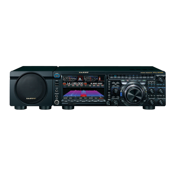
HF/50 MHz TRANSCEIVER
FTDX101MP
FTDX101D
Introduction
This manual provides the technical information necessary
for servicing the FTDX101MP, FTDX101D HF/50 MHz
TRANSCEIVER.
Servicing this equipment requires expertise in handing
surface-mount chip components. Attempts by non-qualified
persons to service this equipment may result in permanent
damage not covered by the warranty, and may be illegal in
some countries.
While we believe the information in this manual to be cor-
rect, YAESU assumes no liability for damage that may oc-
cur as a result of typographical or other errors that may be
present. Your cooperation in pointing out any inconsisten-
cies in the technical information would be appreciated.
This transceiver was assembled using Pb (lead) free solder, based on the RoHS specification.
Only lead-free solder (Alloy Composition: Sn-3.0Ag-0.5Cu) should be used for repairs performed on this apparatus. The solder stated
above utilizes the alloy composition required for compliance with the lead-free specification, and any solder with the above alloy com-
position may be used.
Technical Supplement
Specifications
Board Unit (Schematics, Layouts & Parts)
RX-2 Unit
200W-PA Unit
200W-TUNER Unit
Important Note
EH068H90A
©2020 YAESU MUSEN CO., LTD.
Contents
Advertisement
Table of Contents

Related Manuals for Yaesu FTDX101MP


Summary of Contents for Yaesu FTDX101MP
-
Page 1: Table Of Contents
MAIN Unit While we believe the information in this manual to be cor- RX-1 Unit rect, YAESU assumes no liability for damage that may oc- RX-2 Unit cur as a result of typographical or other errors that may be present. Your cooperation in pointing out any inconsisten- AF Unit cies in the technical information would be appreciated. - Page 2 Power Consumption (Approx.): 3.5 A (FTDX101D) Rx (signal present) 120VA (FTDX101MP) 4 A (FTDX101D) Tx 720VA (FTDX101MP: 200 W) 23 A (FTDX101D: 100 W) 16.6” x 5.1” x 12.7” (420 x 130 x 322 mm) Dimensions (WxHxD): 31.5 ibs (14.3 kg): FTDX101MP Weight (Approx.): 26.5 lbs (12 kg): FTDX101D Transmitter FTDX101MP: 5 - 200 W (5 - 50 W AM carrier) Power Output: FTDX101D: 5 - 100 watts (5 - 25 W AM carrier) J3E (SSB): Balanced, Modulation Types: A3E (AM): Low-Level (Early Stage), F3E (FM): Variable Reactance ±5.0 kHz/±2.5 kHz (Narrow) Maximum FM Deviation: Better than –50 dB (1.8 MHz - 29.7 MHz Amateur bands) Harmonic Radiation: Better than –66 dB (50 MHz Amateur band: 200 W) Better than –63 dB (50 MHz Amateur band: 100 W)
- Page 3 Audio Output Impedance: 4 to 16 Ohms (4 Ohms: nominal) Less than 4 nW Conducted Radiation: Specifications are subject to change, in the interest of technical improvement, without notice or obligation, and are guaranteed only within the amateur bands. FTDX101MP/D Technical Supplement SPESIFICATIONS-2...
- Page 4 Exploded View RA6223700 NAME PLATE(101D) RA6215300 NAME PLATE (101MP) RA6230500 NAME PLATE(YAESU) RA621500B FRONT PANEL(PRT) RA6215400 ESCUTCHEON(ASSY) RA6220000 6 LEVER 5 1 RA138500A VOLUME KNOB(OUT) 1 RA1384900 ① VOLUME KNOB(IN) 2 ① RA6219900 ENCODER KNOB(MULTI) 1 ① RA6218300 ② PORON SHEET(5081) ①...
- Page 5 SPONGE RUBBER(A) RA6216400 ③ RA621700A LIGHT GUIDE(C_R) ③ KNOB ASSY(SPLIT) ③ RA621690A RA6215800 ③ PUSH KNOB(BANDR) REF. YAESU P/N Description Qty. KNOB ASSY(PWR) ① U24206001 BIND HEAD TAPTITE-B M2.6X6 ② U24104001 BIND HEAD TAPTITE-B M2X4 RA622980A KNOB ASSY(FUNC) ③ U24105001 BIND HEAD TAPTITE-B M2X5(3) ④...
- Page 6 ② ② ⑧ RA6261600 (2 pcs) ② PORON SHEET(20X20) ② ⑤ ⑨ CS2589703 (USA: FTDX101D) 1: This parts are attached to ⑧ . (FTDX101MP only) T9207808 1 ⑥ MAIN-UNIT CS2589704 (USA: FTDX101MP) ⑨ WIRE ASSY 1 CS2589705 (EU: FTDX101D) 1 ⑨...
-
Page 7: Exploded View
YAESU P/N Description Qty. WASHER ① U24410007 BIND HEAD TAPTITE-B M4X10B ② ② U9900254 SPECIAL SCREW M4X20B(W/WASHER) ③ U03306002 (FTDX101MP) SEMS SCREW ASM3X6NI CQ0946001 (FTDX101D) RA1507700 R7133800B (FTDX101MP) CQ0946002 (FTDX101MP) WASHER ④ U24206001 BIND HEAD TAPTITE-B M2.6X6 BOTTOM CASE ASSY (FTDX101D) ①... -
Page 8: Block Diagram
Block Diagram BLOCK DIAGRAM-1 FTDX101MP/D Technical Supplement... -
Page 9: Alignment
Digital DC Voltmeter (high-Z, 1 M-Ohm/V) DC Voltmeter DC Ammeter (30 A) Ohmmeter 50-Ohm Dummy Load (100/200 watts) In-Line Wattmeter (150/300 watts, 50-Ohm) Linear Detector RF Coupler 4-Ohm AF Dummy Load (3 watts) 1/4-inch 3-contact Plug Important Notice Do not adjust the alignment menus that are not mentioned in this manual. FTDX101MP/D Technical Supplement ALIGNMENT -1... - Page 10 Alignment VDD Meter Adjustment Connect the DC voltmeter to J6001 on the Press the [MULTI] knob, then rotate the [MPVD] 200W-PA-Unit (FTDX101MP) or TP5005 or ring so that the VDD meter reading is the same TP5006 on the PA-Unit (FTDX101D). as that reading on the DC voltmeter. FTDX101MP: 50.0 V Press and hold in the [MODE], [SSB] and [CW] keys, while turning the radio on, to enter the FTDX101D: 13.8 V Press and hold in the [S.MENU] button to save alignment mode.
- Page 11 Rotate the MAIN DIAL knob so that the fre- the MAIN Unit. quency counter reading is “400.00000 ±20 Hz”. Press and hold in the [MODE], [SSB] and [CW] Press and hold in the [S.MENU] button to save the new setting and exit the alignment mode. keys, while turning the radio on, to enter the alignment mode. Rotate the [MULTI] knob to select the align- ment parameter “1-003 FREQ”. TP1097 FTDX101MP/D Technical Supplement ALIGNMENT -3...
- Page 12 Press and hold in the [MODE], [SSB] and [CW] Release the PTT button. Press and hold in the [S.MENU] button to save keys, while turning the radio on, to enter the the new setting and exit the alignment mode. alignment mode. Rotate the [MULTI] knob to select the align- ment parameter “1-002 TEMP MTR”. Pin 6 of J1002 FTDX101MP/D Technical Supplement ALIGNMENT -4...
- Page 13 Rotate the [MULTI] knob to select the align- ment parameter “2-005 Local 50”. ment parameter “2-001 Local 7”. Press the [MULTI] knob, then rotate the [MPVD] Press the [MULTI] knob, then rotate the [MPVD] ring so that the DC voltmeter reading is “1.00 V ring so that the DC voltmeter reading is “1.10 V (±0 05 V)”. (±0 05 V)”. Set the Main Band frequency to 14.20 MHz. Rotate the [MULTI] knob to select the align- ment parameter “2-002 Local 14”. Press the [MULTI] knob, then rotate the [MPVD] ring so that the DC voltmeter reading is “1.05 V (±0 05 V)”. VR3001 TP3007 TP3006 FTDX101MP/D Technical Supplement ALIGNMENT -5...
- Page 14 2-013 IF-AGC 21 21.200 MHz, 10 dBµ 21.200 MHz -2.0 dB ± 0.5 dB 2-014 IF-AGC 28 28.700 MHz, 7 dBµ 28.700 MHz -2.0 dB ± 0.5 dB 2-015 IF-AGC 50 51.900 MHz, 7 dBµ 51.900 MHz -2.0 dB ± 0.5 dB FTDX101MP/D Technical Supplement ALIGNMENT -6...
- Page 15 Rotate the [MULTI] knob to select the align- alignment mode. Rotate the [MULTI] knob to select the align- ment parameter “2-033 FM SQL TI”. ment parameter “2-029 FM GAIN S1 28”. Press the [MULTI] knob. Rotate the [MPVD] ring so the S-meter reading Press and hold in the [S.MENU] button to save is “S-1”. the new setting and exit the alignment mode. Press and hold in the [S.MENU] button to save the new setting and exit the alignment mode. FTDX101MP/D Technical Supplement ALIGNMENT -7...
- Page 16 IF Trap Adjustment Set the Main Band frequency to 10.100 MHz in the CW-USB mode. Set the following controls as indicated: [ANT] : ANT 1 [IPO] : AMP1 [ATT] : OFF [R.FLT] : 3 kHz [WIDTH] : 2.4 kHz [AGC] : AUTO [RF GAIN] : Fully clockwise Connect the AF millivoltmeter and 4 Ohm dummy load to the EXT SP jack. Connect the RF Signal Generator to the “ANT 1” jack, then set the output level to +40 to +80 dBµ at the 9.005 MHz. Adjust L3125 and VR3002 on the RX-1 Unit for minimum deflection on the AF millivoltmeter. VR3002 L3125 FTDX101MP/D Technical Supplement ALIGNMENT -8...
- Page 17 Set the Sub Band frequency to 50.50 MHz. Press the [MULTI] knob, then rotate the [MPVD] Rotate the [MULTI] knob to select the align- ring so that the DC voltmeter reading is “1.10 V ment parameter “3-005 Local 50”. (±0 05 V)”. Press the [MULTI] knob, then rotate the [MPVD] Set the Sub Band frequency to 14.20 MHz. ring so that the DC voltmeter reading is “1.00 V Rotate the [MULTI] knob to select the align- (±0 05 V)”. ment parameter “3-002 Local 14”. VR4001 TP4007 TP4006 FTDX101MP/D Technical Supplement ALIGNMENT -9...
- Page 18 3-013 IF-AGC 21 21.200 MHz, 10 dBµ 21.200 MHz -2.0 dB ± 0.5 dB 3-014 IF-AGC 28 28.700 MHz, 7 dBµ 28.700 MHz -2.0 dB ± 0.5 dB 3-015 IF-AGC 50 51.900 MHz, 7 dBµ 51.900 MHz -2.0 dB ± 0.5 dB FTDX101MP/D Technical Supplement ALIGNMENT -10...
- Page 19 Rotate the [MULTI] knob to select the align- alignment mode. Rotate the [MULTI] knob to select the align- ment parameter “3-033 FM SQL TI”. ment parameter “3-029 FM GAIN S1 28”. Press the [MULTI] knob. Rotate the [MPVD] ring so the S-meter reading Press and hold in the [S.MENU] button to save is “S-1”. the new setting and exit the alignment mode. Press and hold in the [S.MENU] button to save the new setting and exit the alignment mode. FTDX101MP/D Technical Supplement ALIGNMENT -11...
- Page 20 Set the Sub Band frequency to 10.100 MHz in the CW-USB mode. Set the following controls as indicated: [ANT] : ANT 2 [IPO] : AMP1 [ATT] : OFF [R.FLT] : 3 kHz [WIDTH] : 2.4 kHz [AGC] : AUTO [RF GAIN] : Fully clockwise Connect the AF millivoltmeter and 4 Ohm dummy load to the EXT SP jack. Connect the RF Signal Generator to the “ANT 2” jack, then set the output level to +40 to +80 dBµ at the 8.900 MHz. Adjust L4125 and VR4002 on the RX-2 Unit for minimum deflection on the AF millivoltmeter. VR4002 L4125 FTDX101MP/D Technical Supplement ALIGNMENT -12...
- Page 21 Connect the AF millivoltmeter and 4 Ohm Press and hold in the [S.MENU] button to save dummy load to the EXT SP jack. the new setting and exit the alignment mode. Press the VC TUNE key. Press the VC TUNE Operation key, activate the VC Tune function. VC TUNE key VC TUNE Operation key Adjust TC4804 and TC4810 on the VCT Unit for maximum deflection on the AF millivoltmeter. TC4809 TC4807 TC4802 TC4805 TC4804 TC4806 TC4808 TC4803 TC4801 TC4811 TC4810 FTDX101MP/D Technical Supplement ALIGNMENT -13...
- Page 22 Alignment PA Unit Adjustment (FTDX101MP) Press and hold the PTT button then adjust the VR6002 so that the DC ammeter reading is “800 Preparation mA (±100 mA)”. Connect the 50-Ohm Dummy Load and Watt- Press and hold the PTT button then adjust the meter to the “ANT 1” jack. VR6003 so that the DC ammeter reading is “1.6 Disconnect the coaxial cables from J6001 and A (±200 mA)”.
- Page 23 “4-005 I-ALC 14” for the 14 MHz amateur band's ALC Adjustment. Key the transmitter, then adjusting the [MPVD] ring for 220 W on the Wattmeter. Unkey the transmitter, then rotate the [MPVD] ring so that the parameter indication “4” in- crease. Rotate the [MULTI] knob to select the align- ment parameter “4-006 I-ALC 18” for the 18 MHz amateur band's ALC Adjustment. FTDX101MP/D Technical Supplement ALIGNMENT -15...
- Page 24 Unkey the transmitter, then rotate the holding in the PTT button. [MPVD] ring so that the parameter indica- Release the PTT button, then press and hold in tion “4” in-crease. the [S.MENU] button to save the new setting Press and hold in the [S.MENU] button to save and exit the alignment mode. the new setting and exit the alignment mode. FTDX101MP/D Technical Supplement ALIGNMENT -16...
- Page 25 10 W (+1 W/-0 W) 4-043 10 W 4-079 10 W Maximum deflection Maximum deflection 4-044 4-080 4-045 5 W (+1 W/-0 W) 4-081 5 W (+1 W/-0 W) 4-046 4-082 Maximum deflection Maximum deflection 4-047 4-083 FTDX101MP/D Technical Supplement ALIGNMENT -17...
- Page 26 20 W (+2 W/-0 W) [MPVD] ring Press and hold in the [S.MENU] button to save 4-148 20 W Maximum deflection the new setting and exit the alignment mode. 4-149 4-150 10 W (+1 W/-0 W) 4-151 10 W Maximum deflection 4-152 4-153 5 W (+1 W/-0 W) 4-154 Maximum deflection 4-155 FTDX101MP/D Technical Supplement ALIGNMENT -18...
- Page 27 J5007, then connect the coaxial cables to mA (±10 mA)”. J5001 and J5007. Release the PTT button. Re-connect the jumper plugs to J5004 and J5005. Drive Stage Idling Current Adjustment Connect the DC ammeter to J5005 on the PA Unit. VR5001 VR5005 VR5003 J5001 VR5002 J5004 J5005 VR5004 J5007 FTDX101MP/D Technical Supplement ALIGNMENT -19...
- Page 28 “4-005 I-ALC 14” for the 14 MHz amateur band's ALC Adjustment. Key the transmitter, then adjusting the [MPVD] ring for 110 W on the Wattmeter. Unkey the transmitter, then rotate the [MPVD] ring so that the parameter indication “10” in- crease. Rotate the [MULTI] knob to select the align- ment parameter “4-006 I-ALC 18” for the 18 MHz amateur band's ALC Adjustment. FTDX101MP/D Technical Supplement ALIGNMENT -20...
- Page 29 PTT button. Unkey the transmitter, then rotate the Release the PTT button, then press and hold in [MPVD] ring so that the parameter indica- the [S.MENU] button to save the new setting tion “10” in-crease. and exit the alignment mode. Press and hold in the [S.MENU] button to save the new setting and exit the alignment mode. FTDX101MP/D Technical Supplement ALIGNMENT -21...
- Page 30 10 W (+1 W/-0 W) 4-043 10 W 4-079 10 W Maximum deflection Maximum deflection 4-044 4-080 4-045 5 W (+1 W/-0 W) 4-081 5 W (+1 W/-0 W) 4-046 4-082 Maximum deflection Maximum deflection 4-047 4-083 FTDX101MP/D Technical Supplement ALIGNMENT -22...
- Page 31 5W TXG 70”) as indicated by the chart on the 4-150 10 W (+1 W/-0 W) 4-151 10 W previous page. Maximum deflection 4-152 Press and hold in the [S.MENU] button to save 4-153 5 W (+1 W/-0 W) the new setting and exit the alignment mode. 4-154 Maximum deflection 4-155 FTDX101MP/D Technical Supplement ALIGNMENT -23...
- Page 32 Alignment REV-ALC Adjustment FM MAX Deviation Adjustment Connect the 100-Ohm (FTDX101MP) or 16.6- Connect the Dummy Load, Wattmeter, and De- Ohm (FTDX101D) Dummy Load to the “ANT 1” viation Meter to the “ANT 1” Jack. Set the value of Menu item (RADIO SETTING jack. Press and hold in the [MODE], [SSB] and [CW] → MODE FM → MIC GAIN) “MIC GAIN” to keys, while turning the radio on, to enter the “50”.
- Page 33 SWR-MTR CO 14” and “4-229 SWR-MTR CO 50”. These parameters are always “128”. Press and hold in the [S.MENU] button to save the new setting and exit the alignment mode. Connect the 3-pin plug to J9002 on the AF Unit. Important Notice: If it will be in a transceiver transmitting state, without connecting the 3-pin plug to J9002, there is a possibility that a final transistor may break. FTDX101MP/D Technical Supplement ALIGNMENT -25...
- Page 34 COMP meter. on the DC ammeter Rotate the [MULTI] knob to select the align- Press the [MULTI] key, then unkey the trans- ment parameter “4-233 COMP MTR 30dB”, mitter. then rotate the [MPVD] ring so that the COMP Press and hold in the [S.MENU] button to save meter deflects to full scale. the new setting and exit the alignment mode. Press and hold in the [S.MENU] button to save the new setting and exit the alignment mode. FTDX101MP/D Technical Supplement ALIGNMENT -26...
- Page 35 MAIN Unit Circuit Diagram (MAIN Unit/CPU) FTDX101MP/D Technical Supplement MAIN-1...
- Page 36 MAIN Unit Circuit Diagram (MAIN Unit/DVI) FTDX101MP/D Technical Supplement MAIN-2...
- Page 37 MAIN Unit Circuit Diagram (MAIN Unit/DSP) FTDX101MP/D Technical Supplement MAIN-3...
- Page 38 MAIN Unit Parts Layout (side A) FTDX101MP/D Technical Supplement MAIN-4...
- Page 39 MAIN Unit Parts Layout (side B) FTDX101MP/D Technical Supplement MAIN-5...
-
Page 40: Main Unit
GRM1555C1H102JA01D K22179756 C 1164 CHIP CAP. 0.001uF GRM1555C1H102JA01D K22179756 C 1165 CHIP CAP. 15pF GRM1552C1H150JA01D K22178216 C 1166 CHIP CAP. GRM1552C1H6R0DA01D K22178208 C 1167 CHIP CAP. 0.01uF GRM155R71H103KA88D K22178848 C 1168 CHIP CAP. 0.01uF GRM155R71H103KA88D K22178848 FTDX101MP/D Technical Supplement MAIN-6... - Page 41 K22179756 C 1253 CHIP CAP. 0.1uF GRM155R71H104KE14D K22178872 C 1254 CHIP CAP. 0.1uF GRM155R71H104KE14D K22178872 C 1255 CHIP CAP. 0.1uF GRM155R71H104KE14D K22178872 C 1256 CHIP CAP. 100pF GRM1552C1H101JA01D K22178236 C 1258 CHIP CAP. 10uF GRM188B31A106ME69D K22104810 FTDX101MP/D Technical Supplement MAIN-7...
- Page 42 K22140832 C 1475 CHIP CAP. 10uF GRM188B31A106ME69D K22104810 C 1476 CHIP CAP. 0.1uF GRM155R71H104KE14D K22178872 C 1479 CHIP CAP. 10uF GRM188B31A106ME69D K22104810 C 1480 CHIP CAP. 4.7uF GRM21BB31E475KA75L K22140832 C 1481 CHIP CAP. 0.1uF GRM155R71H104KE14D K22178872 FTDX101MP/D Technical Supplement MAIN-8...
- Page 43 K22178872 C 2014 CHIP CAP. 0.1uF GRM155R71H104KE14D K22178872 C 2015 CHIP CAP. 0.1uF GRM155R71H104KE14D K22178872 C 2016 CHIP CAP. 0.1uF GRM155R71H104KE14D K22178872 C 2017 CHIP CAP. 0.1uF GRM155R71H104KE14D K22178872 C 2018 CHIP CAP. 0.1uF GRM155R71H104KE14D K22178872 FTDX101MP/D Technical Supplement MAIN-9...
- Page 44 K22178872 C 2092 CHIP CAP. 0.1uF GRM155R71H104KE14D K22178872 C 2093 CHIP CAP. 0.1uF GRM155R71H104KE14D K22178872 C 2094 CHIP CAP. 0.1uF GRM155R71H104KE14D K22178872 C 2095 CHIP CAP. 0.1uF GRM155R71H104KE14D K22178872 C 2096 CHIP CAP. 0.1uF GRM155R71H104KE14D K22178872 FTDX101MP/D Technical Supplement MAIN-10...
- Page 45 K22104810 C 2181 CHIP CAP. 0.1uF GRM155R71H104KE14D K22178872 C 2182 CHIP CAP. 10uF GRM188B31A106ME69D K22104810 C 2183 CHIP CAP. 0.1uF GRM155R71H104KE14D K22178872 C 2184 CHIP CAP. 10uF GRM188B31A106ME69D K22104810 C 2185 CHIP CAP. 10uF GRM188B31A106ME69D K22104810 FTDX101MP/D Technical Supplement MAIN-11...
- Page 46 K22104810 C 2260 CHIP TA.CAP. 220uF TMCMB0G227MTRF K78060052 C 2261 CHIP TA.CAP. 220uF TMCMB0G227MTRF K78060052 C 2274 CHIP CAP. GRM155B31A105KE15D K22108809 D 1001 DIODE RB051L-40TE25 G2070718 D 1003 DIODE BAS316 G2070716 D 1004 DIODE 1SV325(TPH3.F) G2070848 FTDX101MP/D Technical Supplement MAIN-12...
- Page 47 L9190133 FB2016 FERRITE BEADS BLM15BD102SN1D L9190133 FB2017 FERRITE BEADS BLM15BD102SN1D L9190133 FB2018 FERRITE BEADS BLM15BD102SN1D L9190133 FB2019 FERRITE BEADS BLM18PG221SN1D L9190181 FB2020 FERRITE BEADS BLM18PG221SN1D L9190181 FB2021 FERRITE BEADS BLM18PG221SN1D L9190181 J 1001 CONNECTOR SC25-12WS P0090631 FTDX101MP/D Technical Supplement MAIN-13...
- Page 48 Q 1016 TRANSISTOR 2SC4081 T106 R G3340818R Q 1017 SN74LVC1G14DCKR G1095586 Q 1018 ADF4001BRUZ-REEL7 G1093977 Q 1019 TRANSISTOR 2SA1576A T106 R G3115768R Q 1020 TRANSISTOR 2SA1576A T106 R G3115768R Q 1021 TPS76301DBVR G1094152 Q 1022 TA75S01F(TE85R.F) G1091593 FTDX101MP/D Technical Supplement MAIN-14...
- Page 49 TPS650250RHBR G1095544 Q 2042 5M160ZE64I5N G1095686 R 1001 CHIP RES. RMC1 150JTE J24305150 R 1002 CHIP RES. 1/16W RMC1/16S 103JTH J24189037 R 1003 CHIP RES. RMC1 6R8JTE J24305689 R 1004 CHIP RES. 1/16W RMC1/16S JPTH J24189070 FTDX101MP/D Technical Supplement MAIN-15...
- Page 50 1.5k 1/16W RMC1/16SK152FTH J24189496 R 1082 CHIP RES. 1/10W RMC1/10T 101J J24205101 R 1083 CHIP RES. 1/10W RMC1/10T 101J J24205101 R 1084 CHIP RES. 1/16W RMC1/16S 103JTH J24189037 R 1085 CHIP RES. 1/16W RMC1/16S 103JTH J24189037 FTDX101MP/D Technical Supplement MAIN-16...
- Page 51 RAC104D103JCTP J42900024 R 1162 CHIP RES. 1/16W RMC1/16S 103JTH J24189037 R 1163 CHIP RES. 4.7k 1/16W RMC1/16S 472JTH J24189033 R 1164 CHIP RES. 4.7k 1/16W RMC1/16S 472JTH J24189033 R 1166 CHIP RES. 1/16W RMC1/16S JPTH J24189070 FTDX101MP/D Technical Supplement MAIN-17...
- Page 52 RMC1/16S JPTH J24189070 R 1253 CHIP RES. 1/16W RMC1/16S JPTH J24189070 R 1254 CHIP RES. 1/16W RMC1/16S JPTH J24189070 R 1255 CHIP RES. 100k 1/16W RMC1/16S 104JTH J24189049 R 1258 CHIP RES. 1/16W RMC1/16S 1R0JTH J24189319 FTDX101MP/D Technical Supplement MAIN-18...
- Page 53 RMC1/16S JPTH J24189070 R 1853 CHIP RES. 1/16W RMC1/16S JPTH J24189070 R 1854 CHIP RES. 4.7k 1/16W RMC1/16S 472JTH J24189033 R 1856 CHIP RES. 1/16W RMC1/16S 680JTH J24189011 R 1857 CHIP RES. 1/16W RMC1/16S 680JTH J24189011 FTDX101MP/D Technical Supplement MAIN-19...
- Page 54 1/16W RMC1/16S JPTH J24189070 R 2077 CHIP RES. 1/16W RMC1/16S 101JTH J24189013 R 2078 CHIP RES. 1/16W RMC1/16S 102JTH J24189025 R 2079 CHIP RES. 1/16W RMC1/16S 103JTH J24189037 R 2080 CHIP RES. 1/16W RMC1/16S 103JTH J24189037 FTDX101MP/D Technical Supplement MAIN-20...
- Page 55 1/16W RMC1/16S 103JTH J24189037 R 2182 CHIP RES. 1/16W RMC1/16S 223JTH J24189041 R 2183 CHIP RES. 1/16W RMC1/16S 103JTH J24189037 R 2184 CHIP RES. 1/16W RMC1/16S 103JTH J24189037 R 2199 CHIP RES. 1/16W RMC1/16S 103JTH J24189037 FTDX101MP/D Technical Supplement MAIN-21...
- Page 56 R 2304 CHIP RES. 100k 1/16W RMC1/16S 104JTH J24189049 R 2305 CHIP RES. 100k 1/16W RMC1/16S 104JTH J24189049 R 2306 CHIP RES. 100k 1/16W RMC1/16S 104JTH J24189049 R 2307 CHIP RES. 100k 1/16W RMC1/16S 104JTH J24189049 FTDX101MP/D Technical Supplement MAIN-22...
- Page 57 CHECK TERMINAL RCTCTE Q5000103 X 1001 XTAL DSX321G 11.1MHz DSX321G 11.100MHZ H0103446 X 1002 XTAL 100MHz SM-532B-100.000MHz H0103480 X 1003 TCXO 40MHz DSA535SG-40.000MHZ H9501950 X 1801 XTAL DSX321G 24MHz DSX321G 24.000MHZ H0103444 XF1001 SAW FILTER NSVS679 H4900032 FTDX101MP/D Technical Supplement MAIN-23...
- Page 58 RX-1 Unit Circuit Diagram FTDX101MP/D Technical Supplement RX-1 -1...
- Page 59 RX-1 Unit Parts Layout side A side B FTDX101MP/D Technical Supplement RX-1 -2...
-
Page 60: Rx-1 Unit
K22178209 C 3078 CHIP CAP. 68pF GRM1552C1H680JA01D K22178232 C 3079 CHIP CAP. GRM1554C1H1R0CA01D K22178202 C 3080 CHIP CAP. 47pF GRM1552C1H470JA01D K22178228 C 3081 CHIP CAP. 12pF GRM1552C1H120JA01D K22178214 C 3082 CHIP CAP. 47pF GRM1552C1H470JA01D K22178228 FTDX101MP/D Technical Supplement RX-1 -3... - Page 61 K22178848 C 3155 CHIP CAP. 0.001uF GRM1555C1H102JA01D K22179756 C 3157 CHIP CAP. GRM155R61E105KE11D K22149010 C 3158 CHIP CAP. 0.001uF GRM1555C1H102JA01D K22179756 C 3159 CHIP CAP. 470pF GRM1555C1H471JA01D K22179748 C 3160 CHIP CAP. 390pF GRM1555C1H391JA01D K22179746 FTDX101MP/D Technical Supplement RX-1 -4...
- Page 62 C 3231 CHIP CAP. 0.01uF GRM155R71H103KA88D K22178848 C 3232 CHIP CAP. 0.01uF GRM155R71H103KA88D K22178848 C 3234 CHIP CAP. 0.1uF GRM155R71H104KE14D K22178872 C 3235 CHIP CAP. 0.01uF GRM155R71H103KA88D K22178848 C 3236 CHIP CAP. 0.1uF GRM155R71H104KE14D K22178872 FTDX101MP/D Technical Supplement RX-1 -5...
- Page 63 K22178224 C 3311 CHIP CAP. 0.0082uF GRM155R71H822KA88D K22178846 C 3312 CHIP CAP. 56pF GRM1552C1H560JA01D K22178230 C 3315 CHIP CAP. GRM1552C1H6R0DA01D K22178208 C 3316 CHIP CAP. 18pF GRM1552C1H180JA01D K22178218 C 3318 CHIP CAP. 100pF GRM1552C1H101JA01D K22178236 FTDX101MP/D Technical Supplement RX-1 -6...
- Page 64 K22178872 C 3398 CHIP CAP. 0.1uF GRM155R71H104KE14D K22178872 C 3400 CHIP CAP. 0.1uF GRM155R71H104KE14D K22178872 C 3401 CHIP CAP. 47pF GRM1552C1H470JA01D K22178228 C 3402 CHIP CAP. GRM1554C1H2R0CA01D K22178204 C 3403 CHIP CAP. 47pF GRM1552C1H470JA01D K22178228 FTDX101MP/D Technical Supplement RX-1 -7...
- Page 65 0.001uF GRM1555C1H102JA01D K22179756 C 3474 CHIP CAP. 0.001uF GRM155B11H102KA01D K22178809 C 3475 AL.ELECTRO.CAP. 220uF EMVA160ADA221MF80G K48120021 C 3476 CHIP CAP. GRM1552C1H9R0DA01D K22178211 C 3477 AL.ELECTRO.CAP. 220uF EMVA160ADA221MF80G K48120021 C 3478 CHIP CAP. 0.01uF GRM155R71H103KA88D K22178848 FTDX101MP/D Technical Supplement RX-1 -8...
- Page 66 C 3552 CHIP CAP. 0.001uF GRM155B11H102KA01D K22178809 C 3553 CHIP CAP. 39pF GRM1552C1H390JA01D K22178226 C 3554 CHIP CAP. 0.01uF GRM155R71H103KA88D K22178848 C 3555 CHIP TA.CAP. 10uF TMCMA1C106MTRF K78120077 C 3556 CHIP CAP. 270pF GRM1552C1H271JA01D K22179715 FTDX101MP/D Technical Supplement RX-1 -9...
- Page 67 C 3638 CHIP CAP. 0.001uF GRM155B11H102KA01D K22178809 C 3639 CHIP CAP. 0.1uF GRM155R71H104KE14D K22178872 C 3640 CHIP CAP. 0.01uF GRM155R71H103KA88D K22178848 C 3641 CHIP CAP. 0.001uF GRM155B11H102KA01D K22178809 C 3642 CHIP CAP. 0.1uF GRM155R71H104KE14D K22178872 FTDX101MP/D Technical Supplement RX-1 -10...
- Page 68 D 3009 DIODE RN142S TE61 G2070994 D 3010 DIODE RN142S TE61 G2070994 D 3011 DIODE RN142S TE61 G2070994 D 3012 DIODE RN142S TE61 G2070994 D 3013 DIODE BAS316 G2070716 D 3014 DIODE RN142S TE61 G2070994 FTDX101MP/D Technical Supplement RX-1 -11...
- Page 69 CHIP COIL 0.15uH C2520C-R15G-RA L1691296 L 3003 CHIP COIL 0.15uH C2520C-R15G-RA L1691296 L 3004 M.RFC 1000uH LLM3225-102J L1691157 L 3005 M.RFC 8.2uH 1008LS-822XJLC L1691482 L 3006 M.RFC 1.8uH 1008LS-182XJLC L1691474 L 3007 M.RFC 1008LS-102XJLC L1691471 FTDX101MP/D Technical Supplement RX-1 -12...
- Page 70 NLV25T-270J-PF L1691441 L 3078 CHIP COIL 0.1uH C2520C-R10G-RA L1691294 L 3079 M.RFC 0.18uH 1008CS-181XGLC L1691673 L 3080 CHIP COIL 27uH NLV25T-270J-PF L1691441 L 3081 CHIP COIL 3.3uH NLV25T-3R3J-PF L1691430 L 3082 M.RFC 1.2uH 1008CS-122XGLC L1691686 FTDX101MP/D Technical Supplement RX-1 -13...
- Page 71 G3070084 Q 3021 TRANSISTOR DTC114EUA T106 G3070084 Q 3022 BU2152FS(TAPE) G1093942 Q 3023 TRANSISTOR DTC114EUA T106 G3070084 Q 3024 TRANSISTOR UMD5N TR G3070343 Q 3025 TRANSISTOR DTC114EUA T106 G3070084 Q 3026 TRANSISTOR UMD5N TR G3070343 FTDX101MP/D Technical Supplement RX-1 -14...
- Page 72 RMC1/16 100JATP J24185100 R 3043 CHIP RES. 1/16W RMC1/16 101JATP J24185101 R 3044 CHIP RES. 1/10W RMC1/10T 330J J24205330 R 3045 CHIP RES. 1/10W RMC1/10T 330J J24205330 R 3046 CHIP RES. 1/10W RMC1/10T 330J J24205330 FTDX101MP/D Technical Supplement RX-1 -15...
- Page 73 RMC1/10T 221J J24205221 R 3119 CHIP RES. 1/10W RMC1/10T 221J J24205221 R 3120 CHIP RES. 8.2k 1/16W RMC1/16 822JATP J24185822 R 3121 CHIP RES. 1/10W RMC1/10T 000J J24205000 R 3122 CHIP RES. 1/16W RMC1/16 331JATP J24185331 FTDX101MP/D Technical Supplement RX-1 -16...
- Page 74 RMC1/16 104JATP J24185104 R 3238 CHIP RES. 1/4W RMC1/4 470JATP J24245470 R 3239 CHIP RES. 1/16W RMC1/16 101JATP J24185101 R 3240 CHIP RES. 1/10W RMC1/10T 000J J24205000 R 3241 CHIP RES. 1/16W RMC1/16 331JATP J24185331 FTDX101MP/D Technical Supplement RX-1 -17...
- Page 75 T 3005 BALUN TRANSFOMERS #458PT-1565 L0190273 T 3006 BALUN TRANSFOMERS 070812736D L0023047 T 3007 BALUN TRANSFOMERS 070812735D L0023046 T 3008 BALUN TRANSFOMERS 070812735D L0023046 T 3009 BALUN TRANSFOMERS 070812735D L0023046 T 3010 BALUN TRANSFOMERS 070812737B L0023048 FTDX101MP/D Technical Supplement RX-1 -18...
- Page 76 9M27C2(9FC2)9.005MHZ H1102524 XF3004 XTAL FILTER 9.005MHz W09F06B-9.005MHZ H1102526A SHIELD CASE (BPF) RA0961600 SHIELD CASE COVER (BPF) RA0961700 SHIELD CASE (33X47) RA0830500 SHIELD CASE COVER (33X47) RA0830600 SHIELD CASE (37x30.5) RA6079500 SHIELD CASE COVER (37x30.5) RA1152400 FTDX101MP/D Technical Supplement RX-1 -19...
- Page 77 RX-2 Unit Circuit Diagram FTDX101MP/D Technical Supplement RX-2 -1...
- Page 78 RX-2 Unit Parts Layout side A side B FTDX101MP/D Technical Supplement RX-2 -2...
- Page 79 K22178209 C 4078 CHIP CAP. 68pF GRM1552C1H680JA01D K22178232 C 4079 CHIP CAP. GRM1554C1H1R0CA01D K22178202 C 4080 CHIP CAP. 47pF GRM1552C1H470JA01D K22178228 C 4081 CHIP CAP. 12pF GRM1552C1H120JA01D K22178214 C 4082 CHIP CAP. 47pF GRM1552C1H470JA01D K22178228 FTDX101MP/D Technical Supplement RX-2 -3...
- Page 80 K22178848 C 4155 CHIP CAP. 0.001uF GRM1555C1H102JA01D K22179756 C 4157 CHIP CAP. GRM155R61E105KE11D K22149010 C 4158 CHIP CAP. 0.001uF GRM1555C1H102JA01D K22179756 C 4159 CHIP CAP. 470pF GRM1555C1H471JA01D K22179748 C 4160 CHIP CAP. 390pF GRM1555C1H391JA01D K22179746 FTDX101MP/D Technical Supplement RX-2 -4...
- Page 81 C 4231 CHIP CAP. 0.01uF GRM155R71H103KA88D K22178848 C 4232 CHIP CAP. 0.01uF GRM155R71H103KA88D K22178848 C 4234 CHIP CAP. 0.1uF GRM155R71H104KE14D K22178872 C 4235 CHIP CAP. 0.01uF GRM155R71H103KA88D K22178848 C 4236 CHIP CAP. 0.1uF GRM155R71H104KE14D K22178872 FTDX101MP/D Technical Supplement RX-2 -5...
- Page 82 K22178224 C 4311 CHIP CAP. 0.0082uF GRM155R71H822KA88D K22178846 C 4312 CHIP CAP. 56pF GRM1552C1H560JA01D K22178230 C 4315 CHIP CAP. GRM1552C1H6R0DA01D K22178208 C 4316 CHIP CAP. 18pF GRM1552C1H180JA01D K22178218 C 4318 CHIP CAP. 100pF GRM1552C1H101JA01D K22178236 FTDX101MP/D Technical Supplement RX-2 -6...
- Page 83 K22178872 C 4398 CHIP CAP. 0.1uF GRM155R71H104KE14D K22178872 C 4400 CHIP CAP. 0.1uF GRM155R71H104KE14D K22178872 C 4401 CHIP CAP. 47pF GRM1552C1H470JA01D K22178228 C 4402 CHIP CAP. GRM1554C1H2R0CA01D K22178204 C 4403 CHIP CAP. 47pF GRM1552C1H470JA01D K22178228 FTDX101MP/D Technical Supplement RX-2 -7...
- Page 84 0.001uF GRM1555C1H102JA01D K22179756 C 4474 CHIP CAP. 0.001uF GRM155B11H102KA01D K22178809 C 4475 AL.ELECTRO.CAP. 220uF EMVA160ADA221MF80G K48120021 C 4476 CHIP CAP. GRM1552C1H9R0DA01D K22178211 C 4477 AL.ELECTRO.CAP. 220uF EMVA160ADA221MF80G K48120021 C 4478 CHIP CAP. 0.01uF GRM155R71H103KA88D K22178848 FTDX101MP/D Technical Supplement RX-2 -8...
- Page 85 C 4552 CHIP CAP. 0.001uF GRM155B11H102KA01D K22178809 C 4553 CHIP CAP. 39pF GRM1552C1H390JA01D K22178226 C 4554 CHIP CAP. 0.01uF GRM155R71H103KA88D K22178848 C 4555 CHIP TA.CAP. 10uF TMCMA1C106MTRF K78120077 C 4556 CHIP CAP. 270pF GRM1552C1H271JA01D K22179715 FTDX101MP/D Technical Supplement RX-2 -9...
- Page 86 C 4639 CHIP CAP. 0.1uF GRM155R71H104KE14D K22178872 C 4640 CHIP CAP. 0.01uF GRM155R71H103KA88D K22178848 C 4641 CHIP CAP. 0.001uF GRM155B11H102KA01D K22178809 C 4642 CHIP CAP. 0.1uF GRM155R71H104KE14D K22178872 C 4643 CHIP CAP. 0.01uF GRM155R71H103KA88D K22178848 FTDX101MP/D Technical Supplement RX-2 -10...
- Page 87 D 4010 DIODE RN142S TE61 G2070994 D 4011 DIODE RN142S TE61 G2070994 D 4012 DIODE RN142S TE61 G2070994 D 4013 DIODE BAS316 G2070716 D 4014 DIODE RN142S TE61 G2070994 D 4015 DIODE RN142S TE61 G2070994 FTDX101MP/D Technical Supplement RX-2 -11...
- Page 88 L 4004 M.RFC 1000uH LLM3225-102J L1691157 L 4005 M.RFC 8.2uH 1008LS-822XJLC L1691482 L 4006 M.RFC 1.8uH 1008LS-182XJLC L1691474 L 4007 M.RFC 1008LS-102XJLC L1691471 L 4008 CHIP COIL 0.56uH C2520C-R56G-RA L1691303 L 4009 M.RFC 0.39uH HA4036-ALC L1692002 FTDX101MP/D Technical Supplement RX-2 -12...
- Page 89 1008CS-181XGLC L1691673 L 4080 CHIP COIL 27uH NLV25T-270J-PF L1691441 L 4081 CHIP COIL 3.3uH NLV25T-3R3J-PF L1691430 L 4082 M.RFC 1.2uH 1008CS-122XGLC L1691686 L 4083 CHIP COIL 15uH NLV25T-150J-PF L1691438 L 4085 M.RFC 47uH LLM3225-470J L1691141 FTDX101MP/D Technical Supplement RX-2 -13...
- Page 90 G1093942 Q 4023 TRANSISTOR DTC114EUA T106 G3070084 Q 4024 TRANSISTOR UMD5N TR G3070343 Q 4025 TRANSISTOR DTC114EUA T106 G3070084 Q 4026 TRANSISTOR UMD5N TR G3070343 Q 4027 TRANSISTOR DTC114EUA T106 G3070084 Q 4028 F2255NLGK8 G1095332 FTDX101MP/D Technical Supplement RX-2 -14...
- Page 91 RMC1/10T 330J J24205330 R 4045 CHIP RES. 1/10W RMC1/10T 330J J24205330 R 4046 CHIP RES. 1/10W RMC1/10T 330J J24205330 R 4047 CHIP RES. 1/10W RMC1/10T 330J J24205330 R 4048 CHIP RES. 1/10W RMC1/10T 330J J24205330 FTDX101MP/D Technical Supplement RX-2 -15...
- Page 92 RMC1/16 822JATP J24185822 R 4121 CHIP RES. 1/10W RMC1/10T 000J J24205000 R 4122 CHIP RES. 1/16W RMC1/16 331JATP J24185331 R 4123 CHIP RES. 1/16W RMC1/16 821JATP J24185821 R 4125 CHIP RES. 1/16W RMC1/16 153JATP J24185153 FTDX101MP/D Technical Supplement RX-2 -16...
- Page 93 RMC1/10T 000J J24205000 R 4241 CHIP RES. 1/16W RMC1/16 331JATP J24185331 R 4242 CHIP RES. 1.8k 1/16W RMC1/16 182JATP J24185182 R 4243 CHIP RES. 1/10W RMC1/10T 100J J24205100 R 4244 CHIP RES. 1/10W RMC1/10T 100J J24205100 FTDX101MP/D Technical Supplement RX-2 -17...
- Page 94 T 4005 BALUN TRANSFOMERS #458PT-1565 L0190273 T 4006 BALUN TRANSFOMERS 070812736D L0023047 T 4007 BALUN TRANSFOMERS 070812735D L0023046 T 4008 BALUN TRANSFOMERS 070812735D L0023046 T 4009 BALUN TRANSFOMERS 070812735D L0023046 T 4010 BALUN TRANSFOMERS 070812737B L0023048 FTDX101MP/D Technical Supplement RX-2 -18...
- Page 95 8M27C(8FC)-8.900MHZ H1102518 XF4004 XTAL FILTER 8.9MHz W08F06A-8.900MHZ H1102520A SHIELD CASE (BPF) RA0961600 SHIELD CASE COVER (BPF) RA0961700 SHIELD CASE (33X47) RA0830500 SHIELD CASE COVER (33X47) RA0830600 SHIELD CASE (37x30.5) RA6079500 SHIELD CASE COVER (37x30.5) RA1152400 FTDX101MP/D Technical Supplement RX-2 -19...
- Page 96 AF Unit Circuit Diagram FTDX101MP/D Technical Supplement AF-1...
- Page 97 AF Unit Parts Layout (side A) FTDX101MP/D Technical Supplement AF-2...
- Page 98 AF Unit Parts Layout (side B) FTDX101MP/D Technical Supplement AF-3...
-
Page 99: Af Unit
JMK107BJ475MA-T K22084803 C 9075 CHIP CAP. 10uF GRM188R61E106MA73D K22144818 C 9076 CHIP CAP. 0.01uF GRM155R71H103KA88D K22178848 C 9077 CHIP CAP. 0.1uF GRM155R71H104KE14D K22178872 C 9078 CHIP CAP. GRM155R61E105KE11D K22149010 C 9079 CHIP CAP. 0.1uF GRM155R71H104KE14D K22178872 FTDX101MP/D Technical Supplement AF-4... - Page 100 10uF TMCMA1C106MTRF K78120077 C 9158 CHIP CAP. 0.01uF GRM155R71H103KA88D K22178848 C 9159 CHIP CAP. 0.001uF GRM155B11H102KA01D K22178809 C 9160 CHIP CAP. GRM155R61E105KE11D K22149010 C 9161 CHIP CAP. 0.0047uF GRM155B11H472KA01D K22178838 C 9162 AL.ELECTRO.CAP. 1000uF 25CE1000BS K48140025 FTDX101MP/D Technical Supplement AF-5...
- Page 101 K78160032 C 9250 CHIP CAP. 0.1uF GRM155R71H104KE14D K22178872 C 9251 CHIP CAP. 22pF GRM1552C1H220JA01D K22178220 C 9252 CHIP CAP. 0.1uF GRM155R71H104KE14D K22178872 C 9253 CHIP TA.CAP. 47uF TAJC476M016RNJ K78120125 C 9254 CHIP CAP. 0.1uF GRM155R71H104KE14D K22178872 FTDX101MP/D Technical Supplement AF-6...
- Page 102 GRM155B11H102KA01D K22178809 C 9330 CHIP CAP. 0.1uF GRM155R71H104KE14D K22178872 C 9331 AL.ELECTRO.CAP. 220uF EEE1AA221XP K48100007 C 9332 CHIP CAP. 0.1uF GRM155R71H104KE14D K22178872 C 9333 CHIP CAP. 0.01uF GRM155R71H103KA88D K22178848 C 9334 CHIP CAP. 0.01uF GRM155R71H103KA88D K22178848 FTDX101MP/D Technical Supplement AF-7...
- Page 103 L9190220 FB9020 FERRITE BEADS BLM15BD182SN1D L9190220 FB9021 FERRITE BEADS BLM15BD182SN1D L9190220 FB9022 FERRITE BEADS BLM15BD182SN1D L9190220 FB9023 FERRITE BEADS BLM15BD182SN1D L9190220 FB9025 FERRITE BEADS BLM15BD182SN1D L9190220 FB9026 FERRITE BEADS BLM15BD182SN1D L9190220 FB9027 FERRITE BEADS BLM15BD182SN1D L9190220 FTDX101MP/D Technical Supplement AF-8...
- Page 104 RTM002P02(TAPE) G3070347 Q 9008 NJM2732V-TE1 G1095466 Q 9009 NJM2732V-TE1 G1095466 Q 9010 CD4066BPWR G1093865 Q 9011 TRANSISTOR 2SC4081 T106 R G3340818R Q 9012 LM2904PWR G1094010 Q 9013 ADM3202ARUZ G1094022 Q 9014 TRANSISTOR 2SC4081 T106 R G3340818R FTDX101MP/D Technical Supplement AF-9...
- Page 105 CHIP RES. 1/16W RMC1/16S JPTH J24189070 R 9011 CHIP RES. 1/16W RMC1/16S 100JTH J24189001 R 9012 CHIP RES. 1/16W RMC1/16S 100JTH J24189001 R 9013 CHIP RES. 1/16W RMC1/16S 103JTH J24189037 R 9014 CHIP RES. 1/16W RMC1/16SK753FTH J24189606 FTDX101MP/D Technical Supplement AF-10...
- Page 106 1/16W RMC1/16S 333JTH J24189043 R 9089 CHIP RES. 1/16W RMC1/16S 470JTH J24189009 R 9090 CHIP RES. 1/16W RMC1/16S 470JTH J24189009 R 9091 CHIP RES. 1/16W RMC1/16S 103JTH J24189037 R 9092 CHIP RES. 1/16W RMC1/16S 103JTH J24189037 FTDX101MP/D Technical Supplement AF-11...
- Page 107 CHIP RES. 1/16W RMC1/16S 471JTH J24189021 R 9169 CHIP RES. 1/16W RMC1/16SK223FTH J24189492 R 9170 CHIP RES. 1/16W RMC1/16S 102JTH J24189025 R 9171 CHIP RES. 1/16W RMC1/16S 470JTH J24189009 R 9173 CHIP RES. 1/16W RMC1/16SK473FTH J24189525 FTDX101MP/D Technical Supplement AF-12...
- Page 108 RMC1/16S 472JTH J24189033 R 9258 CHIP RES. 4.7k 1/16W RMC1/16S 472JTH J24189033 R 9259 CHIP RES. 1/16W RMC1/16S 103JTH J24189037 R 9263 CHIP RES. 1/10W RMC1/10T 000J J24205000 R 9264 CHIP RES. 1/10W RMC1/10T 000J J24205000 FTDX101MP/D Technical Supplement AF-13...
- Page 109 1/16W RMC1/16S 472JTH J24189033 R 9362 CHIP RES. 1/16W RMC1/16S 471JTH J24189021 R 9363 CHIP RES. 1/16W RMC1/16S 470JTH J24189009 R 9364 CHIP RES. 1/4W RMC1/4 331JATP J24245331 R 9365 CHIP RES. 1/16W RMC1/16S 103JTH J24189037 FTDX101MP/D Technical Supplement AF-14...
- Page 110 1/16W RMC1/16S 472JTH J24189033 R 9445 CHIP RES. 1/16W RMC1/16S 103JTH J24189037 R 9446 CHIP RES. 1/16W RMC1/16S 101JTH J24189013 R 9447 CHIP RES. 1/16W RMC1/16S JPTH J24189070 R 9448 CHIP RES. 1/16W RMC1/16S JPTH J24189070 FTDX101MP/D Technical Supplement AF-15...
- Page 111 FTR-B4SA012Z-B05 M1190209 TP9068 CHECK TERMINAL RCTCTE Q5000103 TP9069 CHECK TERMINAL RCTCTE Q5000103 VR9001 POT. VG039NSNXTB103 J51848103 X 9001 XTAL DSX321G 24MHz DSX321G 24.000MHZ H0103444 X 9002 XTAL DSX321G 12MHz DSX321G 12.000MHZ H0103442 HEAT SINK SP141K S5000229 FTDX101MP/D Technical Supplement AF-16...
- Page 112 VCT Unit Circuit Diagram FTDX101MP/D Technical Supplement VCT-1...
- Page 113 VCT Unit Parts Layout side A side B FTDX101MP/D Technical Supplement VCT-2...
-
Page 114: Vct Unit
CHIP CAP. GRM155R61E105KE11D K22149010 C 4886 CHIP CAP. 0.1uF GRM155R71H104KE14D K22178872 C 4887 CHIP CAP. GRM155R61E105KE11D K22149010 C 4888 AL.ELECTRO.CAP. 0.47uF UZS1HR47MCL1GB K48170034 C 4890 AL.ELECTRO.CAP. 100uF EEE1CA101WP K48120012 C 4891 CHIP CAP. 0.1uF GRM155R71H104KE14D K22178872 FTDX101MP/D Technical Supplement VCT-3... - Page 115 Q 4820 TC7S32FU(TE85R.F) G1091529 Q 4821 TRANSISTOR UMD5N TR G3070343 Q 4822 SN74HCT04PWR G1094484 Q 4823 MMBFJ310LT1G G3070457 Q 4826 TRANSISTOR 2SA1576A T106 R G3115768R Q 4827 TRANSISTOR DTC144EUA T106 G3070041 Q 4828 TRANSISTOR DTC144EUA T106 G3070041 FTDX101MP/D Technical Supplement VCT-4...
- Page 116 TZB4R500AA10R00 K91000292 TC4807 TRIMMER CAP. 30pF TZB4P300AA10R00 K91000288 TC4808 TRIMMER CAP. 20pF TZB4R200AA10R00 K91000217 TC4809 TRIMMER CAP. 20pF TZB4R200AA10R00 K91000217 TC4810 TRIMMER CAP. 40pF TZB4P400AA10R00 K91000290 TC4811 TRIMMER CAP. 20pF TZB4R200AA10R00 K91000217 SHIELD CASE (VCT) RA6184200 FTDX101MP/D Technical Supplement VCT-5...
- Page 117 VCT-CNTL Unit Circuit Diagram FTDX101MP/D Technical Supplement VCT-CNTL -1...
- Page 118 VCT-CNTL Unit Parts Layout side A side B FTDX101MP/D Technical Supplement VCT-CNTL -2...
-
Page 119: Vct Cntl Unit
RMC1/16 000JATP J24185000 R 3819 CHIP RES. 1/16W RMC1/16 000JATP J24185000 R 3820 CHIP RES. 1/16W RMC1/16 000JATP J24185000 R 3821 CHIP RES. 1/16W RMC1/16 000JATP J24185000 R 3822 CHIP RES. 1/16W RMC1/16 000JATP J24185000 FTDX101MP/D Technical Supplement VCT-CNTL -3... - Page 120 PA Unit (FTDX101D) Circuit Diagram FTDX101MP/D Technical Supplement PA-1...
- Page 121 PA Unit (FTDX101D) Parts Layout (side A) FTDX101MP/D Technical Supplement PA-2...
- Page 122 PA Unit (FTDX101D) Parts Layout (side B) FTDX101MP/D Technical Supplement PA-3...
-
Page 123: Pa Unit
K22179711 C 5119 CHIP CAP. 270pF GRM1552C1H271JA01D K22179715 C 5120 CHIP CAP. 68pF GRM1552C1H680JA01D K22178232 C 5121 CHIP CAP. 22uF GRM21BR61E226ME44L K22140830 C 5122 CHIP CAP. 0.001uF GRM155B11H102KA01D K22178809 C 5123 CHIP CAP. 0.01uF GRM155R71H103KA88D K22178848 FTDX101MP/D Technical Supplement PA-4... - Page 124 C 5210 CHIP CAP. 0.01uF GRM155R71H103KA88D K22178848 C 5211 CHIP CAP. 0.001uF GRM155B11H102KA01D K22178809 C 5212 CHIP CAP. 180pF 630V GRM31A5C2J181JW01D K22281235 C 5213 CHIP CAP. 0.001uF GRM155B11H102KA01D K22178809 C 5214 CHIP CAP. 0.1uF GRM155R71H104KE14D K22178872 FTDX101MP/D Technical Supplement PA-5...
- Page 125 68pF 630V GRM31A5C2J680JW01D K22281230 C 5313 CHIP CAP. 47pF 630V GRM31A5C2J470JW01D K22281228 C 5314 CHIP CAP. 1000pF 630V GRM31B5C2J102JW01L K22281244 C 5316 CHIP CAP. 120pF 630V GRM31A5C2J121JW01D K22281233 C 5318 CHIP CAP. 47pF 630V GRM31A5C2J470JW01D K22281228 FTDX101MP/D Technical Supplement PA-6...
- Page 126 GRM155R71H104KE14D K22178872 C 5445 CHIP CAP. 0.1uF GRM155R71H104KE14D K22178872 C 5448 AL.ELECTRO.CAP. 10uF EEE1VA100WR K48160006 C 5449 CHIP CAP. 0.1uF GRM155R71H104KE14D K22178872 C 5450 CHIP CAP. 0.001uF GRM155B11H102KA01D K22178809 C 5451 CHIP CAP. 0.01uF GRM155R71H103KA88D K22178848 FTDX101MP/D Technical Supplement PA-7...
- Page 127 LK2125 1R5K-T L1690321 L 5008 M.RFC 0.47uH LK2125 R47K-T L1690315 L 5009 M.RFC 0.68uH LK2125 R68K-T L1690317 L 5010 M.RFC 0.18uH LK2125 R18K-T L1690310 L 5011 M.RFC 6.8uH MLF2012E6R8KT000 L1692058 L 5012 M.RFC 1.5uH LK2125 1R5K-T L1690321 FTDX101MP/D Technical Supplement PA-8...
- Page 128 RMC1/16 000JATP J24185000 R 5009 CHIP RES. 1/16W RMC1/16 471FTP J24183471 R 5011 CHIP RES. 1/16W RMC1/16 000JATP J24185000 R 5018 CHIP RES. 2.2k 1/16W RMC1/16 222JATP J24185222 R 5020 CHIP RES. 1/10W RMC1/10T 331J J24205331 FTDX101MP/D Technical Supplement PA-9...
- Page 129 RR1220P-184-D-C J24209225 R 5098 CHIP RES. 1.5k 1/10W 0.1% RR1220P-152-B J24209078 R 5099 CHIP RES. 1/10W 0.1% RR1220P-103-B J24209098 R 5100 CHIP RES. 100k 1/16W RMC1/16 104JATP J24185104 R 5101 CHIP RES. 1/10W RMC1/10T 330J J24205330 FTDX101MP/D Technical Supplement PA-10...
- Page 130 CHECK TERMINAL RCTCTE Q5000103 VR5001 POT. VG039NCHXTB102 J51846102 VR5002 POT. 2.2k VG039NCHXTB222 J51846222 VR5003 POT. 2.2k VG039NCHXTB222 J51846222 VR5004 POT. 2.2k VG039NCHXTB222 J51846222 VR5005 POT. VG039NCHXTB103 J51846103 VR5006 POT. VG039NCHXTB103 J51846103 SHIELD CASE (19x25) RA6068800 HEATSINK RA6265700 FTDX101MP/D Technical Supplement PA-11...
- Page 131 200W-PA Unit (FTDX101MP) Circuit Diagram FTDX101MP/D Technical Supplement 200W-PA-1...
- Page 132 200W-PA Unit (FTDX101MP) Parts Layout (side A) FTDX101MP/D Technical Supplement 200W-PA-2...
- Page 133 200W-PA Unit (FTDX101MP) Parts Layout (side B) FTDX101MP/D Technical Supplement 200W-PA-3...
- Page 134 200W-PA Unit (FTDX101MP) Parts List DESCRIPTION VALUE TOL. MFR'S DESIG YAESU P/N VERS. LOT SIDE LAY ADR C 6001 CHIP CAP. 0.1uF GRM155R71H104KE14D K22178872 C 6002 CHIP CAP. 0.001uF GRM155B11H102KA01D K22178809 C 6015 CHIP CAP. 0.01uF GRM155R71H103KA88D K22178848 C 6016 CHIP CAP.
- Page 135 200W-PA Unit (FTDX101MP) Parts List DESCRIPTION VALUE TOL. MFR'S DESIG YAESU P/N VERS. LOT SIDE LAY ADR C 6135 CHIP CAP. 270pF GRM1552C1H271JA01D K22179715 C 6136 CHIP CAP. 68pF GRM1552C1H680JA01D K22178232 C 6137 CHIP CAP. 0.001uF GRM155B11H102KA01D K22178809 C 6138 CHIP CAP.
- Page 136 200W-PA Unit (FTDX101MP) Parts List DESCRIPTION VALUE TOL. MFR'S DESIG YAESU P/N VERS. LOT SIDE LAY ADR C 6226 CHIP CAP. 0.018uF GRM155B11E183KA61D K22148835 C 6228 CHIP CAP. 0.001uF GRM155B11H102KA01D K22178809 C 6229 CHIP CAP. 0.01uF GRM155R71H103KA88D K22178848 C 6230 CHIP CAP.
- Page 137 200W-PA Unit (FTDX101MP) Parts List DESCRIPTION VALUE TOL. MFR'S DESIG YAESU P/N VERS. LOT SIDE LAY ADR C 6311 CHIP CAP. 560pF 630V GRM31A5C2J561JW01D K22281241 C 6312 CHIP CAP. 68pF 630V GRM31A5C2J680JW01D K22281230 C 6313 CHIP CAP. 22pF 630V GRM31A5C2J220JW01D...
- Page 138 200W-PA Unit (FTDX101MP) Parts List DESCRIPTION VALUE TOL. MFR'S DESIG YAESU P/N VERS. LOT SIDE LAY ADR C 6393 FILM CAP. 500V UC232H0080D-T K33279005 C 6394 CHIP CAP. 0.1uF 250V GRM32DR72E104KW01L K22245801 C 6395 CHIP CAP. 0.01uF GRM155R71H103KA88D K22178848 C 6396 CHIP CAP.
- Page 139 200W-PA Unit (FTDX101MP) Parts List DESCRIPTION VALUE TOL. MFR'S DESIG YAESU P/N VERS. LOT SIDE LAY ADR FB6005 RFC WITH BEADS 3A RI5.8X6.4-2 L1020732 FB6006 RFC WITH BEADS 3A RI5.8X6.4-2 L1020732 FB6007 FERRITE BEADS BLM18BD601SN1D L9190143 J 6001 CONNECTOR U.FL-R-SMT(10)
- Page 140 200W-PA Unit (FTDX101MP) Parts List DESCRIPTION VALUE TOL. MFR'S DESIG YAESU P/N VERS. LOT SIDE LAY ADR Q 6018 TRANSISTOR UMD5N TR G3070343 Q 6019 TRANSISTOR UMD5N TR G3070343 Q 6020 VRF150 G3090156 Q 6021 VRF150 G3090156 Q 6022 TRANSISTOR...
- Page 141 200W-PA Unit (FTDX101MP) Parts List DESCRIPTION VALUE TOL. MFR'S DESIG YAESU P/N VERS. LOT SIDE LAY ADR R 6086 CHIP RES. 1/10W RMC1/10T 223J J24205223 R 6087 CHIP RES. 2.2k 1/10W RMC1/10T 222J J24205222 R 6088 CHIP RES. 1/16W RMC1/16 221JATP...
- Page 142 200W-PA Unit (FTDX101MP) Parts List DESCRIPTION VALUE TOL. MFR'S DESIG YAESU P/N VERS. LOT SIDE LAY ADR T 6002 COIL 10WIDE BC-278 L0022857 T 6003 COIL PWR-WIDE D12A1T RIB10 L0023112 T 6004 COIL PWR-WIDE D12A TR16 L0022068 T 6005 COIL PWR-WIDE...
- Page 143 TUNER Unit (FTDX101D) Circuit Diagram FTDX101MP/D Technical Supplement TUNER-1...
- Page 144 TUNER Unit (FTDX101D) Parts Layout (side A) FTDX101MP/D Technical Supplement TUNER-2...
- Page 145 TUNER Unit (FTDX101D) Parts Layout (side B) FTDX101MP/D Technical Supplement TUNER-3...
-
Page 146: Tuner Unit
K00359037 C 5574 CERAMIC CAP. 10pF CC45SL3FD100JYNNA K00359037 C 5575 CERAMIC CAP. 10pF CC45SL3FD100JYNNA K00359037 C 5576 CERAMIC CAP. 10pF CC45SL3FD100JYNNA K00359037 C 5577 CHIP CAP. 250V GQM2195C2E6R0CB12D K22240259 C 5578 CHIP CAP. 56pF GRM1552C1H560JA01D K22178230 FTDX101MP/D Technical Supplement TUNER-4... - Page 147 G2070716 D 5533 DIODE BAS316 G2070716 D 5534 DIODE BAS316 G2070716 D 5535 DIODE BAS316 G2070716 D 5536 DIODE BAS316 G2070716 D 5537 DIODE BAS316 G2070716 D 5538 DIODE BAS316 G2070716 D 5539 DIODE BAS316 G2070716 FTDX101MP/D Technical Supplement TUNER-5...
- Page 148 1/16W RMC1/16 101JATP J24185101 R 5504 CHIP RES. 1/16W RMC1/16 471JATP J24185471 R 5505 CHIP RES. 1/16W RMC1/16 220JATP J24185220 R 5506 CHIP RES. 1/16W RMC1/16 471JATP J24185471 R 5507 CHIP RES. 1/16W RMC1/16 471JATP J24185471 FTDX101MP/D Technical Supplement TUNER-6...
- Page 149 RL5516 RELAY DC12V AGQ200A12Z DC12V M1190188 RL5517 RELAY FTR-F3AA012E-(F) M1190224 RL5518 RELAY FTR-F3AA012E-(F) M1190224 RL5519 RELAY FTR-F3AA012E-(F) M1190224 RL5520 RELAY FTR-F3AA012E-(F) M1190224 RL5521 RELAY FTR-F3AA012E-(F) M1190224 RL5522 RELAY FTR-F3AA012E-(F) M1190224 RL5523 RELAY DC12V G5Q-14 DC12V M1190199 FTDX101MP/D Technical Supplement TUNER-7...
- Page 150 FTR-F3AA012E-(F) M1190224 RL5534 RELAY FTR-F3AA012E-(F) M1190224 RL5535 RELAY FTR-F3AA012E-(F) M1190224 RL5536 RELAY FTR-F3AA012E-(F) M1190224 RL5537 RELAY DC12V FTR-B4SA012Z-B05 M1190209 T 5501 BALUN TRANSFOMERS 100812913A L0023088 TC5501 TRIMMER CAP. 20pF TZB4R200AA10R00 K91000217 TP5508 CHECK TERMINAL RCTCTE Q5000103 FTDX101MP/D Technical Supplement TUNER-8...
- Page 151 200W-TUNER Unit (FTDX101MP) Circuit Diagram FTDX101MP/D Technical Supplement 200W-TUNER-1...
- Page 152 200W-TUNER Unit (FTDX101MP) Parts Layout (side A) FTDX101MP/D Technical Supplement 200W-TUNER-2...
- Page 153 200W-TUNER Unit (FTDX101MP) Parts Layout (side B) FTDX101MP/D Technical Supplement 200W-TUNER-3...
- Page 154 200W-TUNER Unit (FTDX101MP) Parts List DESCRIPTION VALUE TOL. MFR'S DESIG YAESU P/N VERS. LOT SIDE LAY ADR C 6501 CHIP CAP. GRM1554C1H2R0CA01D K22178204 C 6502 CHIP CAP. 0.01uF GRM155R71H103KA88D K22178848 C 6503 CHIP CAP. 0.1uF GRM155R71H104KE14D K22178872 C 6504 AL.ELECTRO.CAP.
- Page 155 200W-TUNER Unit (FTDX101MP) Parts List DESCRIPTION VALUE TOL. MFR'S DESIG YAESU P/N VERS. LOT SIDE LAY ADR C 6578 CHIP CAP. 56pF GRM1552C1H560JA01D K22178230 C 6579 CHIP CAP. 68pF GRM1552C1H680JA01D K22178232 C 6580 CERAMIC CAP. 10pF CC45SL3FD100JYNNA K00359037 C 6581 CERAMIC CAP.
- Page 156 200W-TUNER Unit (FTDX101MP) Parts List DESCRIPTION VALUE TOL. MFR'S DESIG YAESU P/N VERS. LOT SIDE LAY ADR D 6522 DIODE BAS316 G2070716 D 6523 DIODE BAS316 G2070716 D 6524 DIODE BAS316 G2070716 D 6525 DIODE BAS316 G2070716 D 6526 DIODE...
- Page 157 200W-TUNER Unit (FTDX101MP) Parts List DESCRIPTION VALUE TOL. MFR'S DESIG YAESU P/N VERS. LOT SIDE LAY ADR Q 6525 TRANSISTOR UMD5N TR G3070343 Q 6526 TRANSISTOR UMD5N TR G3070343 Q 6527 TRANSISTOR UMD5N TR G3070343 Q 6528 TRANSISTOR UMD5N TR...
- Page 158 200W-TUNER Unit (FTDX101MP) Parts List DESCRIPTION VALUE TOL. MFR'S DESIG YAESU P/N VERS. LOT SIDE LAY ADR R 6558 CHIP RES. 100k 1/16W RMC1/16 104JATP J24185104 R 6559 CHIP RES. 3.3k 1/16W RMC1/16 332JATP J24185332 R 6560 CHIP RES. 1/16W...
- Page 159 DISPLAY Unit Circuit Diagram FTDX101MP/D Technical Supplement DISPLAY-1...
- Page 160 DISPLAY Unit Parts Layout (side A) FTDX101MP/D Technical Supplement DISPLAY-2...
- Page 161 DISPLAY Unit Parts Layout (side B) FTDX101MP/D Technical Supplement DISPLAY-3...
-
Page 162: Display Unit
GRM1552C1H8R0DA01D K22178210 C 8539 CHIP CAP. 390pF GRM155B11H391KA01D K22178804 C 8540 CHIP CAP. 0.1uF GRM155R71H104KE14D K22178872 C 8541 CHIP TA.CAP. 47uF TAJC476M016RNJ K78120125 C 8542 AL.ELECTRO.CAP. 220uF RV-16V221MG10-R K48120015 C 8543 CHIP CAP. 0.1uF GRM155R71H104KE14D K22178872 FTDX101MP/D Technical Supplement DISPLAY-4... - Page 163 C 8620 CHIP CAP. 4.7uF 6.3V JMK107BJ475MA-T K22084803 C 8621 CHIP CAP. 0.1uF GRM155R71H104KE14D K22178872 C 8622 CHIP CAP. 0.01uF GRM155R71H103KA88D K22178848 C 8623 CHIP CAP. 0.01uF GRM155R71H103KA88D K22178848 C 8624 CHIP CAP. 22uF 6.3V GRM21BB30J226ME38L K22080806 FTDX101MP/D Technical Supplement DISPLAY-5...
- Page 164 TMCMA1C106MTRF K78120077 C 8780 CHIP CAP. 100pF GRM1552C1H101JA01D K22178236 C 8781 CHIP TA.CAP. 4.7uF TMCMC1V475MTRF K78160036 C 8782 CHIP TA.CAP. 4.7uF TMCMC1V475MTRF K78160036 C 8784 CHIP CAP. 0.01uF GRM155R71H103KA88D K22178848 C 8785 CHIP CAP. GRM155R61E105KE11D K22149010 FTDX101MP/D Technical Supplement DISPLAY-6...
- Page 165 L1690843 FB8436 FERRITE BEADS BLM15AG121SN1D L1690843 FB8437 FERRITE BEADS BLM18PG221SN1D L9190181 FB8438 FERRITE BEADS BLM18PG221SN1D L9190181 FB8439 FERRITE BEADS BLM18PG221SN1D L9190181 FB8440 FERRITE BEADS BLM18PG221SN1D L9190181 FB8441 FERRITE BEADS BLM18PG221SN1D L9190181 FB8442 FERRITE BEADS BLM18PG221SN1D L9190181 FTDX101MP/D Technical Supplement DISPLAY-7...
- Page 166 TRANSISTOR DTC114YUA T106 G3070298 Q 8714 TRANSISTOR DTC114YUA T106 G3070298 Q 8715 TRANSISTOR DTC114YUA T106 G3070298 Q 8716 TRANSISTOR DTC114YUA T106 G3070298 Q 8717 TC74VHC123AFT(TAPE) G1094003 Q 8718 SN74LVC2G08DCTR G1094341 Q 8719 TRANSISTOR DTC114YUA T106 G3070298 FTDX101MP/D Technical Supplement DISPLAY-8...
- Page 167 CHIP RES. RMC1 4R7JTE J24305479 R 8491 CHIP RES. 1/16W RMC1/16S 103JTH J24189037 R 8492 CHIP RES. 1/16W RMC1/16S 102JTH J24189025 R 8493 CHIP RES. 1/16W RMC1/16S 103JTH J24189037 R 8494 CHIP RES. 1/16W RMC1/16S 103JTH J24189037 FTDX101MP/D Technical Supplement DISPLAY-9...
- Page 168 1/16W RMC1/16S 220JTH J24189005 R 8579 CHIP RES. 1/16W RMC1/16S 102JTH J24189025 R 8580 CHIP RES. 1/16W RMC1/16S 102JTH J24189025 R 8581 CHIP RES. 1/16W RMC1/16S 102JTH J24189025 R 8582 CHIP RES. 1/16W RMC1/16S 102JTH J24189025 FTDX101MP/D Technical Supplement DISPLAY-10...
- Page 169 1/16W RMC1/16S 223JTH J24189041 R 8681 CHIP RES. 1/16W RMC1/16S 223JTH J24189041 R 8682 CHIP RES. 1/16W RMC1/16S 103JTH J24189037 R 8683 CHIP RES. 1/16W RMC1/16S 103JTH J24189037 R 8684 CHIP RES. 1/16W RMC1/16S 103JTH J24189037 FTDX101MP/D Technical Supplement DISPLAY-11...
- Page 170 CHECK TERMINAL RCTCTE Q5000103 X 8402 XTAL DSX321G 48MHz 48.000MHZ H0103486 X 8403 XTAL DSX321G 27MHz 27.000MHZ H0103484 X 8404 XTAL SC-32S 32.768kHz SC-32S 32.768KHZ H0103464 SHIELD CASE (28X61) RA6239100 SHIELD CASE RA0060200 BUSTERAID (12.5X10) RA6115700 FTDX101MP/D Technical Supplement DISPLAY-12...
-
Page 171: Memory Unit
1/16W RMC1/16S 220JTH J24189005 R 7006 CHIP RES. 1/16W RMC1/16S 220JTH J24189005 R 7007 CHIP RES. 1/16W RMC1/16S 220JTH J24189005 R 7008 CHIP RES. 1/16W RMC1/16S 220JTH J24189005 R 7009 CHIP RES. 1/16W RMC1/16S JPTH J24189070 FTDX101MP/D Technical Supplement MEMORY-1... - Page 172 SW-A Unit Circuit Diagram FTDX101MP/D Technical Supplement SW-A -1...
- Page 173 SW-A Unit Parts Layout (side A) FTDX101MP/D Technical Supplement SW-A -2...
- Page 174 SW-A Unit Parts Layout (side B) FTDX101MP/D Technical Supplement SW-A -3...
-
Page 175: Sw-A Unit
D 7237 16-219A/T2D-AR2T1QY/3T G2071652 D 7238 16-219A/T2D-AR2T1QY/3T G2071652 D 7239 19-217/GHC-YR1S2/3T G2071438 D 7240 19-213/S2C-AP1Q2B/3T G2071558 D 7242 HT-193TW5 G2071390 D 7243 19-213/S2C-AP1Q2B/3T G2071558 D 7244 16-213/BHC-AN1P2/3T G2071650 D 7245 19-213/S2C-AP1Q2B/3T G2071558 D 7246 16-213/BHC-AN1P2/3T G2071650 FTDX101MP/D Technical Supplement SW-A -4... - Page 176 D 7317 DIODE BAS316 G2070716 D 7318 DIODE BAS316 G2070716 J 7201 CONNECTOR 06FLT-SM2-TB(LF)(SN) P1091255 J 7202 CONNECTOR 06FLT-SM2-TB(LF)(SN) P1091255 J 7203 CONNECTOR 40FLT-SM2-TB(LF)(SN)(M) P1091251 J 7204 CONNECTOR 30FLT-SM2-TB(LF)(SN)(M) P1091142 J 7205 CONNECTOR SC25-04WS P0090623 FTDX101MP/D Technical Supplement SW-A -5...
- Page 177 R 7257 CHIP RES. 1/16W RMC1/16 821JATP J24185821 R 7258 CHIP RES. 2.2k 1/16W RMC1/16 222JATP J24185222 R 7259 CHIP RES. 2.2k 1/16W RMC1/16 222JATP J24185222 R 7260 CHIP RES. 2.2k 1/16W RMC1/16 222JATP J24185222 FTDX101MP/D Technical Supplement SW-A -6...
- Page 178 RMC1/16 102JATP J24185102 R 7335 CHIP RES. 1/16W RMC1/16 102JATP J24185102 R 7336 CHIP RES. 1/16W RMC1/16 102JATP J24185102 R 7337 CHIP RES. 1/16W RMC1/16 102JATP J24185102 R 7338 CHIP RES. 1/16W RMC1/16 102JATP J24185102 FTDX101MP/D Technical Supplement SW-A -7...
- Page 179 S 7248 TACTILE SWITCH EVQPLHA15 N5090174 S 7249 TACTILE SWITCH EVQPLHA15 N5090174 S 7250 TACTILE SWITCH EVQPLHA15 N5090174 S 7251 TACTILE SWITCH EVQPLHA15 N5090174 S 7252 TACTILE SWITCH EVQPLHA15 N5090174 S 7253 TACTILE SWITCH EVQPLHA15 N5090174 FTDX101MP/D Technical Supplement SW-A -8...
-
Page 180: Sw-B Unit
SW-B Unit Circuit Diagram Parts Layout side A side B FTDX101MP/D Technical Supplement SW-B -1... - Page 181 TACT SWITCH SKSMAFE010 N5090186 S 7403 TACT SWITCH SKSMAFE010 N5090186 S 7404 TACT SWITCH SKSMAFE010 N5090186 S 7405 TACT SWITCH SKSMAFE010 N5090186 S 7406 TACT SWITCH SKSMAFE010 N5090186 S 7407 TACT SWITCH SKSMAFE010 N5090186 PLATE R0154650 FTDX101MP/D Technical Supplement SW-B -2...
-
Page 182: Sw-C Unit
SW-C Unit Circuit Diagram Parts Layout side A side B FTDX101MP/D Technical Supplement SW-C -1... - Page 183 J 7503 CONTACT OG-503040 S5000243 Q 7502 TRANSISTOR DTC114EUA T106 G3070084 R 7504 CHIP RES. 2.7k 1/16W RMC1/16 272JATP J24185272 R 7505 CHIP RES. 2.7k 1/16W RMC1/16 272JATP J24185272 S 7501 TACTILE SWITCH EVQPLHA15 N5090174 FTDX101MP/D Technical Supplement SW-C -2...
-
Page 184: Vr Unit
VR Unit Circuit Diagram Parts Layout side A side B FTDX101MP/D Technical Supplement VR-1... - Page 185 R 7601 CHIP RES. 1/16W RMC1/16S JPTH J24189070 R 7602 CHIP RES. 1/16W RMC1/16 103JATP J24185103 R 7603 CHIP RES. 1/16W RMC1/16 103JATP J24185103 VR7601 POT. RH96D1144 25F RY-10302 J62800152 VR7602 POT. RH96D1144 25F RY-10302 J62800152 FTDX101MP/D Technical Supplement VR-2...
-
Page 186: Enc-A Unit
ENC-A Unit Circuit Diagram Parts Layout side A side B Parts List DESCRIPTION VALUE TOL. MFR'S DESIG YAESU P/N VERS. LOT SIDE LAY ADR J 7701 CONNECTOR 06FLT-SM2-TB(LF)(SN) P1091255 S 7701 ROTARY ENCODER RH90D265AE20-25F Q9001052 FTDX101MP/D Technical Supplement ENC-A -1... -
Page 187: Enc-B Unit
ENC-B Unit Circuit Diagram FTDX101MP/D Technical Supplement ENC-B -1... - Page 188 ENC-B Unit Parts Layout side A side B FTDX101MP/D Technical Supplement ENC-B -2...
- Page 189 RMC1/16S 332JTH J24189031 R 7832 CHIP RES. 3.3k 1/16W RMC1/16S 332JTH J24189031 S 7801 ROTARY ENCODER RH90D265AE20-25F Q9001052 S 7802 ROTARY ENCODER RH90D265AE20-25F Q9001052 S 7803 ROTARY ENCODER RH90D265AE20-25F Q9001052 S 7804 ROTARY ENCODER RH90D265AE20-25F Q9001052 FTDX101MP/D Technical Supplement ENC-B -3...
-
Page 190: Jack Unit
JACK Unit Circuit Diagram Parts Layout side A side B FTDX101MP/D Technical Supplement JACK-1... - Page 191 WIRE ASSY AH031H 60MM4P T9207444 R 8101 CHIP RES. 1/16W RMC1/16 000JATP J24185000 R 8102 CHIP RES. 1/16W RMC1/16 000JATP J24185000 R 8103 CHIP RES. 1/16W RMC1/16 000JATP J24185000 FITTING MET41-0191 S5000329 GROUND PLATE (JACK) RA1173300 FTDX101MP/D Technical Supplement JACK-2...
-
Page 192: Mic Unit
MIC Unit Circuit Diagram Parts Layout side A side B FTDX101MP/D Technical Supplement MIC-1... - Page 193 SB20-02WS P0090609 JP8201 WIRE ASSY AH046H 130MM6P T9207565A R 8201 CHIP RES. 1/16W RMC1/16 000JATP J24185000 R 8202 CHIP RES. 1/16W RMC1/16 000JATP J24185000 R 8203 CHIP RES. 1/16W RMC1/16 000JATP J24185000 GROUND PLATE (MIC) RA1173200 FTDX101MP/D Technical Supplement MIC-2...
-
Page 194: Enc-C Unit
K22178809 C 7904 CHIP CAP. 0.001uF GRM155B11H102KA01D K22178809 JP7901 WIRE ASSY AH068H-67MM4P T9207836A R 7901 CHIP RES. 1/16W RMC1/16S 151JTH J24189015 R 7902 CHIP RES. 1/16W RMC1/16S 151JTH J24189015 S 7901 ROTARY ENCODER KE2N22-45 Q9001054 FTDX101MP/D Technical Supplement ENC-C -1... - Page 195 Copyright 2020 YAESU MUSEN CO., LTD. All rights reserved. No portion of this manual may be reproduced without the permission of YAESU MUSEN CO., LTD. YAESU MUSEN CO., LTD. Tennozu Parkside Building 2-5-8 Higashi-Shinagawa, Shinagawa-ku, Tokyo 140-0002 Japan YAESU USA 6125 Phyllis Drive, Cypress, CA 90630, U.S.A.
Need help?
Do you have a question about the FTDX101MP and is the answer not in the manual?
Questions and answers
Как войти в сервисное меню трансивера ?