Table of Contents
Advertisement
T M
1 1 - 6 6 2 5 - 2 9 5 8 - 1 4 & P
TECHNICAL MANUAL
OPERATOR'S, ORGANIZATIONAL,
DIRECT SUPPORT AND GENERAL SUPPORT
MAINTENANCE MANUAL
(INCLUDING REPAIR PARTS
AND SPECIAL TOOLS LIST)
FOR
POWER SUPPLY PP-7545/U
(HEWLETT-PACKARD MODEL 6269B)
(NSN 6130-00-148-1796)
HEADQUARTERS, DEPARTMENT OF THE ARMY
21 AUGUST 1980
Advertisement
Table of Contents
Troubleshooting

Related Manuals for HP 6269B


Summary of Contents for HP 6269B
- Page 1 1 1 - 6 6 2 5 - 2 9 5 8 - 1 4 & P TECHNICAL MANUAL OPERATOR’S, ORGANIZATIONAL, DIRECT SUPPORT AND GENERAL SUPPORT MAINTENANCE MANUAL (INCLUDING REPAIR PARTS AND SPECIAL TOOLS LIST) POWER SUPPLY PP-7545/U (HEWLETT-PACKARD MODEL 6269B) (NSN 6130-00-148-1796) HEADQUARTERS, DEPARTMENT OF THE ARMY 21 AUGUST 1980...
- Page 2 S A F E T Y S T E P S F O L L O W S O M E O N E T H E V I C T I M E L E C T R I C A L S H O C K N O T T R Y...
- Page 3 G E N E R A L S U P P O R T M A I N T E N A N C E M A N U A L (INCLUDING REPAIR PARTS AND SPECIAL TOOLS LISTS) DC POWER SUPPLY PP-7545/U (HEWLETT-PACKARD MODEL 6269B) (NSN 6130-00-148-1796) FOR SERIALS 1027A00101 AND ABOVE*...
-
Page 4: 60Hz Operation)
2-19 Connections for 208 Volt 4-68 Additional Protection Features Operation (Model 6260B and 6269B) MAINTENANCE ....5-1 2-21 Connections for 115 Volt Introduction... -
Page 5: Table Of Contents
TABLE OF CONTENTS (Continued) S e c t i o n Page No. S e c t i o n Page No. V MAINTANCE . . Continued 5-111 Crowbar Disablement 5-22 5-103 Preregulator Tracking (5 O and 60Hz Operation) 5-21 VI REPLACEABLE PARTS . - Page 6 Figure 1-1 DC Power Supply, Model 6259B, 6260B, 6261B, 6268B, or 6269B ... .. l-l 2-1 Outline Diagram ............2-1 2-2 Bias Transformer Primary Connections for 208Vac and 115Vac Operation .
- Page 7 H e w l e t t - P a c k - 18\MCO P4610.19C and DLAR 4500.15. ard (HP) Model 6269B DC Power 0-4. REPORTING EQUIPMENT s u p p l y .
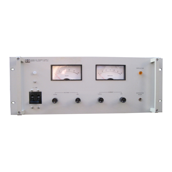
- Page 8 TM 1 1 - 6 6 2 5 - 2 9 5 8 - 1 4 & P SECTION I GENERAL INFORMATION Figure 1-1. DC Power Supply, Model 6259B, 6260B, 6261B, 6268B, or 6269B 1-1 DESCRIPTION 1-4 The power supply has rear output terminals.
-
Page 9: 1-7 Specifications
TM 11-6625-2958-14&P may be used in series when a higher output voltage Option No. Description is required in the constant voltage mode of opera- Three Digit Graduated Decadial Cur- t ion or when greater voltage compliance is required rent Control: A single control that in the constant current mode of operation. - Page 10 Hewlett-Packard field office (see list at rear of this manual for addresses). Specify the 1-15 One manual is shipped with each power sup- model number, serial number prefix, and HP part ply. Additional manuals may be purchased from number shown on the title page.
-
Page 11: Outline Diagram
It is necessary only to connect the in- nominal 230 volt, 208 volt, or 115 volt 57-63Hz strument to a source of power and it is ready for power source. Model 6269B may be operated from operation. a 230 volt or 208 volt, 57-63Hz power source only. -
Page 12: Power Transformer Primary Connections For 208Vac And 115Vac Operation
(Model 6260B and 6269B: Option 027) 6268B, and 6269B) and 115Vac Operation (Except Model 6269B) 2-20 To convert Model 6260B or 6269B to operation from a 208Vac source, taps on the power and bias transformers must be changed as follows: b. - Page 13 2-5 B). Replace cover on RFI assembly. Option 016 in Table 6-4 (Replaceable Parts) for d. Unsolder wires from circuit breaker power ratings and HP Part Numbers. New transfor- A5CB1 and fan B2 connected to "230V" terminal of mer has two primary terminals. Transfer wire from bias transformer A3T2 (see Figure 7-2).
- Page 14 TM 11-6625-2958-14&P b. Perform Steps (b) through (e) of Paragraph grounded) and be of sufficient wire size to handle 2-22. the input current drawn by the supply (see Paragraph 2-16). Note that when the supply is operated from a 115Vac source, the input current is approximately 2-25 CONNECTIONS FOR 50Hz OPERATION double that shown in Paragraph 2-16.
- Page 15 SECTION Ill OPERATING INSTRUCTIONS Figure 3-1. Front Panel Controls and Indicators,’ Modal 6259B, 6260B, 6261B, 6268B or 6269B 3-1 TURN-ON CHECKOUT PROCEDURE 3-3 OPERATING MODES 3-2 The following checkout procedure describes 3-4 The power supply is designed so that its mode...
- Page 16 The trip voltage range is as follows: of down-programming - either turning the VOLTAGE 6 2 6 1 B 6268B, 6269B 6259B, 6260B controls fully counterclockwise, activating the 2 to 12Vdc 2 to 23Vdc...
- Page 17 TM 11-6625-2958-14&P 3-26 The output voltage of the supply should be then proceed at a slower rate towards zero. The actual time required for the output to fall from two -15mV ±5mV when zero ohms is connected across volts to zero will vary from several seconds to the programming terminals.
-
Page 18: Remote Voltage Programming, Non-Unity Gain (Constant Voltage)
4 ohms/ampere resistor should be a low noise, low 6268B 6 ohms/ampere temperature coefficient type. Not e 6269B 4 ohms/ampere that when this resistor is used, the The programming coefficient is determined by the resistance value actually programming constant current programming current which is ad- the supply is the parallel combination justed to within 10% of 2.5mA at the factory. -
Page 19: Remote Voltage Programming, Non-Unity Gain (Constant Current)
3-42 Remote sensing is used to maintain good reg- 6268B 16.7mV/ampere ulation at the load and reduce the degradation of 6269B 10.0mV/ampere regulation which would occur due to the voltage The current required from the voltage source will be drop in the leads between the power supply and the less than 20µA. - Page 20 0.5 volt. If a larger drop must be tolerated, please consult an HP Sales Engineer. NOTE Due to the voltage drop in the load...
- Page 21 TM 11-6625-2958-14&P current greater than that available from one supply. Auto-Parallel operation permits equal current shar- ing under all load conditions, and allows complete control of the output current from one master power supply. The output current of each slave will be approximately equal to the master’s output current regardless of the load conditions.
- Page 22 TM 11-6625-2958-14&P on the maximum voltage rating of the "master" sup- ply. The value of R is this voltage divided by the voltage programming current of the slave supply (1/Kp where K is the voltage programming coeffi- cient). The voltage contribution of the slave is determined by its voltage control setting.
- Page 23 TM 11-6625-2958-14&P c. A large surge current causing a high pow- over from constant voltage to constant current op- eration, or the reverse, in response to an increase er dissipation in the load occurs when the load re- (over the preset limit) in the output current or volt- sistance is reduced rapidly.
-
Page 24: Overall Block Diagram
TM 11-6625-2958-14&P SECTION IV PRINCIPLES OF OPERATION Figure 4-1. Overall Block Diagram 4-1 OVERALL BLOCK DIAGRAM DISCUSSION basis of these inputs, determines at what time each firing pulse is generated. 4-2 The major circuits of the power supply are 4-4 The phase adjusted output of the triac is ap- shown on the overall block diagram of Figure 4-1. - Page 25 TM 11-6625-2958-14&P 4-6 The feedback signals controlling the conduc- tion of the series regulator originate within the constant voltage or constant current comparator. During constant voltage operation the constant voltage comparator continuously compares the out- put voltage of the supply with the drop across the VOLTAGE controls.
- Page 26 1 1 - 6 6 2 5 - 2 9 5 8 - 1 4 & P the supply and, if it exceeds approximately 120% of maximum rated output, sends a turn-down signal to the preregulator control circuit. Hence, the out- put voltage of the supply is limited to a “safe”...
-
Page 27: Preregulator Control Circuit Waveforms
TM 1 1 - 6 6 2 5 - 2 9 5 8 - 1 4 & P waveform (C) of Figure 4-4, the firing pulse is ing current to the summing point, ensuring that the quite narrow because Q73 saturates rapidly, causing triac will fire at low output “voltages. - Page 28 TM 11-6625-2958-14&P during rapid down-programming; diodes CR5 and The input capacitor then begins to discharge through the series regulator, and the voltage across the CR6 prevent excessive voltage excursions from regulator decreases until Q20 turns off. The dis- over-driving the differential amplifier. Capacitor charge time (typically ½...
- Page 29 11-6625-2958-14&P and optional resistor R 117. The other input of the 4-46 MIXER AND ERROR AMPLIFIERS differential amplifier (pin 4) is connected to a sum- ming point (terminal A6) at the junction of the pro- 4-47 The mixer and error amplifiers amplify the gramming resistors and the current pullout resistors error signal from the constant voltage or constant R30 and R31.
- Page 30 TM 11-6625-2958-14&P output. When A4CR110 is fired, overvoltage lamp plied to the series regulator. This negative voltage A5DS2 is tuned on, completing a path for a + 11V keeps the regulator cut off untill C35 charges up. unregulated holding current through A5DS2. This Diode CR37 provides a discharge path for C35 when current holds A4CR110 on even after the output the supply is turned off.
- Page 31 TM 11-6625-2958-14&P 4-68 ADDITIONAL PROTECTION FEATURES tions of output voltage and current on the dc volt- meter and ammeter. Both meter movements can 4-69 The supply contains several “special pur- withstand an overload of many times the maximum pose” components which protect the supply in the rated output without damage.
-
Page 32: 5-3 Test Equipment Required
Variable Range: 207-253Vac. Recommend- Voltage ed minimum output current: 12A, regulation measurement. Transformer 6259B; 22A, 6261B and 6268B; 24A, 6260B: 36A, 6269B. 403B AC Voltmeter Measure ac voltages and Sensitivity: 1mV full scale de- flection (min). Accuracy: 2%. ripple. DC Voltmeter... -
Page 33: Differential Voltmeter Substitute Test Setup
TM 11-6625-2958-14&P Table 5-1. Test Equipment Required (Continued) REQUIRED RECOMMENDED TYPE CHARACTERISTICS MODEL - - - - Terminating Value: 50 ohms, ½ watt, ±5%, Noise spike measure- Resistors non-inductive. (Four required.) ment. - - - - Blocking Value: 0.01µF, 100Vdc. (Two Noise spike measure- Capacitors required.) -
Page 34: Constant Voltage Load Regulation Test Setup
6259B,6260B 1.2mV imum rated output voltage. 6261B 2.2mV e. Differential voltmeter should indicate the 6268B, 6269B 4.2mV following: 10 ±0.2Vdc 6259B, 6260B 5-15 Ripple and Noise. 20 ±0.4Vdc 6261B Definition: The residual ac voltage 40 ±0.8Vdc... - Page 35 TM 1 1 - 6 6 2 5 - 2 9 5 8 - 1 4 & P wire between the negative output terminal of the power supply and the vertical input of the scope, and the grounded scope case. Any ground current circulating in this loop as a result of the difference in potential EG between the two ground points causes an IR drop which is in series with the scope...
-
Page 36: Noise Spike Measurement Test Setup
5. Since the impedance matching resistors 6259B, 6260B, 6261B 500µVrms and 5mV p-p constitute a 2-to-1 attenuator, the noise spikes 6268B, 6269B 1mVrms and 5mV p-p observed on the oscilloscope should be less than 2.5mV p-p instead of 5mV p-p. -
Page 37: Transient Recovery Time Test Setup
TM 11-6625-2958-14&P switch in series with the load is not adequate, 5-32 To check the transient recovery time, pro- since the resulting one-shot displays are difficult ceed as follows: to observe on most oscilloscopes, and the arc a. Connect test setup shown in Figure 5-5. energy occurring during switching action completely b. - Page 38 (Most HP power supplies are rated for oper- the power supply being measured. Typically, a ation from 0°C to 55°C.) The power supply must be supply may drift Iess over the eight hour measure- ment interval than during the half-hour warm-up.
-
Page 39: Current Sampling Resistor Connections
11-6625-2958-14&P Figure 5-7. Current Sampling Resistor Connections NOTE When using the HP current sampling resistor recommended for this instru- ment, an external fan must be employed to cool the resistor. This precaution will maintain the sampling resistance at a constant value. -
Page 40: Constant Current Ripple And Noise Test Setup
6261B 250µVrms 6268B 334µVrms 250µVrms 6269B 5-51 TROUBLESHOOTING 5-52 Before attempting to troubleshoot this instru- ment, ensure that the fault is with the instrument and not with an associated circuit. The perform- ance test (Paragraph 5-5) enables this to be deter- mined without having to remove the instrument from the cabinet. -
Page 41: Overall Troubleshooting
TM 11-6625-2958-14&P al procedure. ) If the trouble source cannot be de- 5-56 OVERALL TROUBLESHOOTING PROCEDURE tected by visual inspection, re-install the main circuit board and proceed to Step (2). 5-57 To locate the cause of trouble, follow Steps 1, 2, and 3 in sequence: (2) In almost all cases, the trouble can be (1) Check for obvious troubles such as trip- caused by incorrect dc bias or reference voltages;... - Page 42 TM 11-6625-2958-14&P Table 5-3. Overall Troubleshooting (Continued) PROBABLE CAUSE SYMPTOM current comparator circuit (Z1 and associated components). High ripple (continued) Improper measurement technique. Refer to Paragraph 5-13. Poor line regulation b. Incorrect reference and/or bias voltages. Refer to Table 5-2. Improper measurement technique.
-
Page 43: Feedback Loop Isolation
TM 11-6625-2958-14&P the supply in order to gain access to components 5-7, the circuit is checked by starting with the (such as the series regulator transistors) that are output waveform and tracing backwards. not mounted on the main circuit board. If this is the case, refer as necessary to Paragraphs 5-65 5-61 Performing the tests given in Table 5-5, 5-6, through 5-70 for disassembly procedures. -
Page 44: Series Regulator Troubleshooting, High Voltage Condition
TM 11-6625-2958-14&P Table 5-5. Series Regulator Troubleshooting, High Voltage Condition PROBABLE CAUSE ACTION RESPONSE STEP in Table 5-4, Step 3. external source connected as described These tests should be made with a. One or more of A4QI03 a. Output voltage remains high. Check turn-off of series through A4Q108 shorted regulator transistors A4Q103... -
Page 45: Series Regulator Troubleshooting, Low Voltage Condition
TM 11-6625-2958-14&P Table 5-6. Series Regulator Troubleshooting, Low Voltage Condition (Continued) STEP ACTION RESPONSE PROBABLE CAUSE Check conduction of driver a. Output voltage remains low. a. A4Q102 open, thermal A4Q102 by shorting A4Q101 switch A4TS101 open. emitter (TP100) to base b. -
Page 46: Preregulator Troubleshooting
TM 11-6625-2958-14&P Table 5-7. Preregulator Troubleshooting (Continued) STEP ACTION RESPONSE PROBABLE CAUSE a. Normal waveform. Connect oscilloscope be- Defective T70. tween TP85 (+) and TP103 b. Little or no voltage. b. Defective Q72, Q73, (-). CR76, or C71. pro- ceed to Step 3. Connect oscilloscope be- a. - Page 47 TM 11-6625-2958-14&P unsoldered at this point. are arrowed “E” and “F“ in Figure 7-1.) Lifting Remove mounting nuts from A4CR106 on brackets away from heat sink allows access to left side of heat sink, and from A4CR108 on right triac A2CR1. A magnetized screwdriver is useful side of heat sink.
-
Page 48: Checks And Adjustments After Replacement Of Semiconductor Devices
TM 11-6625-2958-14&P Table 5-8. Checks and Adjustments After Replacement of Semiconductor Devices REFERENCE FUNCTION OR CIRCUIT CHECK ADJUST Constant voltage and con- Constant voltage (CV) line and load reg- R110, or stant current differential uIation. Zero volt output. R113 (OP- amplifiers. - Page 49 TM 11-6625-2958-14&P Table 5-8. Checks and Adjustments After Replacement of Semiconductor Devices (Continued) REFERANCE FUNCTION OR CIRCUIT CHECK ADJUST - - - Limiting action and level. R70, R82 Output voltage, ripple imbalance, and preregulator waveforms. Crowbar. Trip voltage, voltage across series regu- R95, CR90 thru lator when crowbar is tripped, supply...
- Page 50 TM 11-6625-2958-14&P 5-81 CONSTANT VOLTAGE PROGRAMMING voltage programming. CURRENT Perform Steps (a) and (b) in Paragraph 5-83. b. Rotate CURRENT controls fully clockwise 5-82 Zero Output Voltage. To calibrate the zero voltage programming accuracy, proceed as direct- and turn on supply. ed in Paragraphs 5-83, 5-84, 5-85, or 5-86, If reading on differential 1 voltmeter is not whichever applies to your particular instrument.
- Page 51 180 Ω d. Rotate VOLTAGE controls fully clockwise 6268B 200 Ω and turn on supply. 6269B e. Adjust decade resistance box until dif- ferential voltmeter reads exactly zero volts. d. Connect decade resistance box in place Replace decade resistance box with...
- Page 52 1.33 Ω, 1200W, ±5% 0.3Vdc. 6268B 0.8 Ω, 2000W, ±5% 6269B g. To check the voltage drop at high output voltage, remove short circuit from acress load re- b. Connect variable auto transformer be- sistor and adjust VOLTAGE controls for maximum...
-
Page 53: Maximum Crowbar Trip Voltage
6261B 23Vdc output voltage of the supply. 45Vdc 6268B 6269B 45Vdc 5-109 MAXIMUM CROWBAR TRIP VOLTAGE e. Adjust decade resistance box until crow- bar trips (amber OVERVOLTAGE lamp lights up). 5-110 To adjust the maximum voltage at which the... -
Page 54: Reference Designators
TM 11-6625-2958-14&P SECTION VI REPLACEABLE PARTS 6-1 INTRODUCTION Table 6-1. Reference Designators (Continued) 6-2 This section contains information for ordering = plug . vacuum tube, = transistor replacement parts. Table 6-4 lists parts in alpha- neon bulb, numeric order by reference designators and provides = resistor photocell, etc. - Page 55 TM 11-6625-2958-14&P Table 6-3. Code List of Manufacturers CODE CODE MANUFACTURER ADDRESS MANUFACTURER ADDRESS 00629 EBY Sales Co. , Inc. Jamaica, N. Y. 07138 Westinghouse Electric Corp. 00656 Aerovox Corp. New Bedford, Mass. Electronic Tube Div. Elmira, N. Y. 07263 Fairchild Camera and Instrument 00853 Sangamo Electric Co.
- Page 56 TM 11-6625-2958-14&P Table 6-3. Code List of Manufacturers (Continued) CODE CODE MANUFACTURER ADDRESS MANUFACTURE R ADDRESS 16758 Delco Radio Div. of General Motors Corp. 70563 Amperite Co. Inc. Union City, N. J. 70901 Beemer Engrg. Co. Kokomo, I.nd. Fort Washington, Pa. 17545 Atlantic Semiconductors, Inc.
- Page 57 TM 11-6625-2958-14&P Table 6-3. Code List of Manufacturers (Continued) CODE CODE ADDRESS ADDRESS MANUFACTURER MANUFACTURER 83508 Grant Pulley and Hardware Co. 76530 Cinch City of Industry, Calif. West Nyack, N. Y. 768.54 Oak Mfg. Co. Div. of Oak Electro/Netics Corp. Crystal Lake, III.
- Page 58 TM 11-6625-2958-14&P Table 6-4. Replaceable Parts REF. MFR. DESCRIPTION MFR. PART NO. DESIG. PART NO. CODE Al MAIN PRINTED CIRCUIT BOARD Printed Circuit Board, Main 28480 5060-6189 fxd, mylar. 01µF 200V 28480 0160-0161 fxd, elect. 5µF 50Vdc 30D505G050BB2 0180-0301 56289 fxd, elect.
- Page 59 10 Ω ±5% ½W EB-1005 01121 0686-1005 fxd, comp 200k Ω ±5% ½W EB-2045 01121 0686-2045 var. ww 250 Ω ±10%, Ammeter Adj. R101 Type 110-F4 11236 2100-0439 fxd, met. film 909 Ω ±1% 1/8W R102 Type CEA T-O 07716 0757-0422 6269B...
- Page 60 .125 Ω ±5% 5W R106 28480 0811-1846 fxd, cupron 0.01 Ω 20ppm, Cur- R123 rent Sampling 28480 5080-7144 R150-R155 Emitter Resistor Assembly 28480 06260-60023 fxd, wire helix O.1 Ω ±5% - Part of Emitter Resistor Assembly 28480 0811-2545 6269B...
- Page 61 Cover, Rear Control Barrier Strip 28480 00712-20001 Bus Bar, Output 28480 5000-6252 Barrier Block, AC Input 75382 0360-1596 603-3 Rubber Bumper 2097-W 87585 0403-0089 Spacer, Insulated, AC Input Barrier (2), Output Bus Bars (4) 28480 0380-0710 7120-1111 Serial I.D. Plate 28480 6269B...
- Page 62 Bushing, Potentiometer R125 28480 1410-0052 Nut, Hexagon, R125 28480 2950-0034 Locknut, R121-R124 28480 0590-0013 Bezel, Gray Plastic, 2¼" Mod. 28480 4040-0296 Spring, M1, M2 28480 1460-0256 Handle, 7“ 28480 5020-5762 Machine Screw, Fillister Phillips Head, 10-32x 1-3/4 28480 2680-0173 6269B...
- Page 63 23K Ω ±1% 1\8W 07716 0698-3269 Type CEA T-O R115 var. ww 5k Ω 28480 2100-0806 R116 fxd, met. film 200k Ω ±1% 1/8W Type CEA T-O 07716 0757-0472 R118 var. ww 5k Ω 2100-0806 R119 28480 7124-1721 Label, Identification 6269B 6-10...
- Page 64 07716 0698-3269 R116 VAR. WW 5KΩ 28480 2100-0806 R118 FXD, MET. FILM 200KW ±1% 1/8W TYPE CEA T-O 07716 0757-0472 R119 VAR. WW 5KW 28480 2100-0806 LABEL, IDENTIFICATION 28480 7124-1721 OPTION 027 208VAC INPUT LABEL, IDENTIFICATION 28480 7124-1717 6269B 6-11...
- Page 65 TM11-6625-2958-14&P TABLE 6-5. PART NUMBER - NATIONAL STOCK NUMBER CROSS REFERENCE INDEX NATIONAL NATIONAL PART STOCK PART STOCK NUMBER FSCM NUMBER NUMBER FSCM NUMBER 0150-0052 28480 5910-00-797-4909 0757-0437 28480 5905-00-904-4404 0160-0161 28480 5910-00-911-9271 0757-0440 28480 5905-00-858-6795 0160-0162 28480 5910-00-850-2162 0757-0460 28480 5905-00-858-8959 0160-0168...
-
Page 66: Part Number-National Stock Number Cross Reference Index
PART NUMBER - NATIONAL STOCK NUMBER TM 11-6625-2958-14&P CROSS REFERENCE INDEX NATIONAL NATIONAL PART STOCK PART STOCK NUMBER FSCM NUMBER NUMBER FSCM NUMBER 2100-0806 28480 5905-00-929-0485 2100-1824 28480 5905-00-892-9626 2100-1857 28480 5905-00-575-8853 2100-1866 28480 5905-00-110-0282 242E1025 56289 5905-00-504-4892 243E5005 56289 5905-00-950-5551 2950-0034 28480... -
Page 67: Circuit Diagrams & Component Location Diagrams
TM 11-6625-2958-14&P SECTION Vll CIRCUIT DIAGRAMS AND COMPONENT LOCATION DIAGRAMS This section contains the circuit diagrams neces- b. Preregulator control circuit waveforms sary for the operation and maintenance of this (Figure 7-9), showing the waveforms found at vari- power supply. Included are: ous points in the preregulator control circuit. -
Page 68: A2 Rfi Assembly Component Location Diagram
TM 11-6625-2958-14&P A 2 R F I A s s e m b l y C o m p o n e n t L o c a t i o n D i a g r a m F i g u r e 7 - 1 . (Shown removed from supply with assembly cover off.) F i g u r e 7 - 2 . -
Page 69: Top Front Chassis Assembly Component Location Diagram
TM 11-6625-2958-14&P F i g u r e 7 - 3 . T o p F r o n t C h a s s i s A s s e m b l y C o m p o n e n t L o c a t i o n D i a g r a m... -
Page 70: Bottom Front Chassis Assembly Component Location Diagram
TM 11-6625-2958-14&P F i g u r e 7 - 4 . B o t t o m F r o n t C h a s s i s A s s e m b l y C o m p o n e n t L o c a t i o n D i a g r a m... - Page 71 TM 11-6625-2958-14&P F i g u r e 7 - 5 . B o t t o m R e a r C h a s s i s A s s e m b l y C o m p o n e n t L o c a t i o n D i a g r a m 7 - 5...
- Page 72 TM 11-6625-2958-14&P F i g u r e 7 - 6 . Series Regulator Emitter Resistor A s s e m b l y C o m p o n e n t L o c a t i o n D i a g r a m (Circuit board is part of A4 heat sink assembly.) F i g u r e 7 - 7 .
- Page 73 TM 11-6625-2958-14&P A 4 H e a t S i n k A s s e m b l y C o m p o n e n t L o c a t i o n D i a g r a m F i g u r e 7 - 8 .
- Page 74 Figure 7-10 This publication does not contain Figure 7-10. Figure 7-10 does not exist in paper or digital form. NOT DIGITIZED...
- Page 75 T M 1 1 - 6 6 2 5 - 2 9 5 8 - 1 4 & P APPENDIX A REFERENCES DA Pam 310-4 I n d e x o f T e c h n i c a l M a n u a l s , T e c h n i c a l B u l l e t i n s , Supply Manuals (Types 7, 8 and 9), Supply B u l l e t i n s , a n d L u b r i c a t i o n O r d e r s .
- Page 76 TM 11-6625-2958-14&P A P P E N D I X B COMPONENTS OF END ITEM LIST INTRODUCTION Section L (2) Item number. The number used to iden- B-1. Scope tify item called out in the illustration. This appendix lists integral components of and basic issue items for the PP-7545/U to help b.
- Page 77 SECTION II INTEGRAL COMPONENTS OF END ITEM TM 11-6625-2958-14&P SECTION III BASIC ISSUE ITEMS ILLUSTRATION NATIONAL DESCRIPTION LOCATION USABLE QUANTITY STOCK REQD ITEM NUMBER CODE RCVD DATE PART NUMBER (FSCM) 6130-00-148-1796 PP-7545/U 28480 TM 11-6625-2958-14&P...
- Page 78 TM 11-6625-2958-14&P APPENDIX D MAINTENANCE ALLOCATION Section L INTRODUCTION in precision measurement. Consists of compari- D - 1 . G e n e r a l sons of two instruments, one of which is a certified This appendix provides a summary of the main- standard of known accuracy, to detect and adjust tenance operations f o r t h e P P - 7 5 4 5 / U .
- Page 79 TM 11-6625-2958-14&P D-3. Column Entries e. Column 5, Tools and Equipment. Column 5 specifies by code, those common tool sets (not u. Column 1, Group Number. Column 1 lists individual tools) and special tools, test, and sup- group numbers, the purpose of which is to identify port equipment required to perform the designated components, assemblies, subassemblies, and mod- function.
- Page 80 SECTION II MAINTENANCE ALLOCATION C TM 11-6625-2958-14&P D - 3...
- Page 81 TM11-6625-2958-14&P SECTION III TOOL AND TEST EQUIPMENT REQUIREMENTS POWER SUPPLY PP-7545/U TOOL OR TEST EQUIPMENT MAINTENANCE NOMENCLATURE NATIONAL/NATO TOOL NUMBER REF CODE CATEGORY STOCK NUMBER MULTIMETER AN/URM-105 6625-00-581-2036 TOOL KIT, ELECTRONIC EQUIPMENT TK-101/G 5180-00-064-5178 H, D TOOL KIT, ELECTRONIC EQUIPMENT TK-105/G 5180-00-610-8177 H, D GENERATOR, SIGNAL SG-321/U...
- Page 82 SECTION IV. REMARKS TM 11-6625-2958-14&P POWER SUPPLY PP-7545/U REFERENCE CODE REMARKS Exterior Operational Interior...
-
Page 83: Schematic Diagram
Figure 7-11. Schematic Diagram, Model 6269B... - Page 84 SERIAL MAKE Assembly: CHANGES C2: Add, 0.047µF, 600V, HP Part No. 0160-0005. Prefix Number R2: Add, 220 Ω, ±5%, 2W, HP Part No. 0811-1763. Errata In the Replaceable Parts Iist, make the following 1027A 0245, 0246, changes: 0255 CR1: Delete Mfr. Part No. and change HP Part...
- Page 85 Overvoltage Protection Crowbar circuit), make the following changes: C91: Add, 0.0047µF, 200V, HP Part No. 0160- 0157. R99: Change to 10k Ω, ±5%, ½W, HP Part No. 0686-1035. T70, T90: Change to HP Part No. 5080-7192. The above changes have been made to improve the...
- Page 86 In the parts list under A4 Heat Sink Assembly, failure under short circuit conditions. On sche- change the HP Part No. of CR101, 102, 105, and matic, in the Constant Voltage Comparator Cir- 108 to 1901-0318, and change CR103, 104, and cuit disconnect anode of A1CR6 from A1Z1 pin 1 106 to 1901-0317.
- Page 87 Manual Changes/Model 6269B Manual HP Part No. 06269-90002 Page -4- In the parts list, delete the entire listing under A schematic of RFI Filter Assembly 06269-60010 A2 RFI Filter Assembly and replace with the fol- is shown below. This schematic replaces the A2 lowing.
- Page 90 By Order of the Secretary of the Army: E. C. MEYER General, United States Army Chief of Staff Official: J. C. PENNINGTON Major General, United States Army The Adjutant General Distribution: Active Army: TSG (1) USAERDAA (1) USAERDAW (1) USAARENBD (1) USAINSCOM (2) Army Dep (1) except TRADOC (2)
- Page 94 THE METRIC SYSTEM AND EQUIVALENTS...
- Page 95 PIN: 046413-000...
- Page 96 This fine document... Was brought to you by me: Liberated Manuals -- free army and government manuals Why do I do it? I am tired of sleazy CD-ROM sellers, who take publicly available information, slap “watermarks” and other junk on it, and sell it. Those masters of search engine manipulation make sure that their sites that sell free information, come up first in search engines.
Need help?
Do you have a question about the 6269B and is the answer not in the manual?
Questions and answers