ST STM32 User Manual
Nucleo-64 boards
Hide thumbs
Also See for STM32:
- User manual (85 pages) ,
- Application note (49 pages) ,
- Quick start manual (31 pages)
Table of Contents
Advertisement
UM1724
User manual
STM32 Nucleo-64 boards (MB1136)
Introduction
The STM32 Nucleo-64 boards based on the MB1136 reference board (NUCLEO-F030R8,
NUCLEO-F070RB, NUCLEO-F072RB, NUCLEO-F091RC, NUCLEO-F103RB,
NUCLEO-F302R8, NUCLEO-F303RE, NUCLEO-F334R8, NUCLEO-F401RE,
NUCLEO-F410RB, NUCLEO-F411RE, NUCLEO-F446RE, NUCLEO-L010RB,
NUCLEO-L053R8, NUCLEO-L073RZ, NUCLEO-L152RE
NUCLEO-L452RE,
,
NUCLEO-L476RG
provide an affordable and flexible way for users to try out new concepts
)
and build prototypes with the STM32 microcontrollers in the LQFP64 package, choosing
from the various combinations of performance, power consumption, and features. The
®
ARDUINO
Uno V3 connectivity support and the ST morpho headers provide an easy
means of expanding the functionality of the Nucleo open development platform with a wide
choice of specialized shields. The STM32 Nucleo boards do not require any separate probe
as they integrate the ST-LINK/V2-1 debugger and programmer. The STM32 Nucleo boards
come with the comprehensive free software libraries and examples available with the
®
™
STM32Cube MCU Packages, as well as direct access to the Arm
Mbed
online resources
at http://mbed.org/.
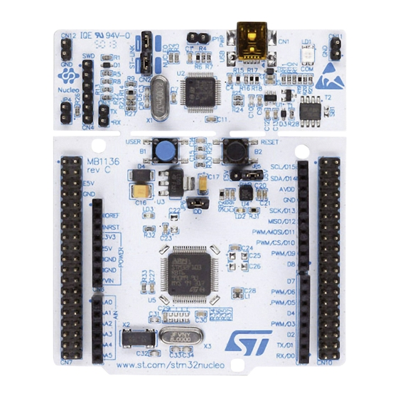
Figure 1. STM32 Nucleo-64 board
Picture is not contractual.
August 2020
UM1724 Rev 14
1/68
www.st.com
1
Advertisement
Table of Contents

Related Manuals for ST STM32


Summary of Contents for ST STM32
-
Page 1: Figure 1. Stm32 Nucleo-64 Board
Nucleo open development platform with a wide choice of specialized shields. The STM32 Nucleo boards do not require any separate probe as they integrate the ST-LINK/V2-1 debugger and programmer. The STM32 Nucleo boards come with the comprehensive free software libraries and examples available with the ®... -
Page 2: Table Of Contents
Embedded ST-LINK/V2-1 ........16... - Page 3 ST morpho connector ........
- Page 4 ST morpho connector on NUCLEO-F030R8 ........
- Page 5 STM32 Nucleo board mechanical dimensions ........15...
-
Page 6: Features
• Two types of extension resources ® – ARDUINO Uno V3 connectivity – ST morpho extension pin headers for full access to all STM32 I/Os • Flexible board power supply: – USB VBUS or external source (3.3 V, 5 V, 7-12 V) –... -
Page 7: Ordering Information
UM1724 Ordering information Ordering information To order an STM32 Nucleo-64 board, refer to Table 1. Additional information is available from the datasheet and reference manual of the target STM32. Table 1. Ordering information Board Order code Targeted STM32 Differentiating feature... -
Page 8: Codification
UM1724 Codification The meaning of the codification is explained in Table Table 2. Codification explanation NUCLEO-XXYYRT Description Example: NUCLEO-L452RE MCU series in STM32 Arm STM32L4 Series Cortex MCUs in the STM32 product line STM32L452 series STM32 package pin count 64 pins STM32 Flash memory size: –... -
Page 9: Development Environment
SBx connections closed by solder or 0-ohm resistor Solder bridge SBx OFF SBx connections left open In this document, the references are “STM32 Nucleo board” and “STM32 Nucleo boards” for all information that is common to all sale types. ®... -
Page 10: Quick Start
USB driver available from the www.st.com/stm32nucleo web page, prior to connecting the board. Connect the STM32 Nucleo board to a PC with a USB cable ‘Type-A to Mini-B’ through USB connector CN1 to power the board. The red LED LD3 (PWR) and LD1 (COM) must light up. -
Page 11: Hardware Configuration Variants
V 0.9 patch package from the www.st.com website and load ‘Bootloader V9.0 CAN patch’ to the STM32, following the information in readme.txt file available in the package. Hardware configuration variants The board can be delivered with different configurations of the oscillator of the target STM32. -
Page 12: Hardware Layout And Configuration
Hardware layout and configuration UM1724 Hardware layout and configuration The STM32 Nucleo board is designed around the STM32 microcontrollers in a 64-pin LQFP package. Figure 2 shows the connections between the STM32 and its peripherals (ST-LINK/V2-1, ® push-button, LED, ARDUINO connectors, and ST morpho connector). -
Page 13: Figure 3. Top Layout
(Red LED) (Green LED) power ® ARDUINO ® ARDUINO connector connector ST morpho CN10 connector ST morpho connector ARDUINO ® connector ® ARDUINO connector 32 KHz crystal(1) STM32 microcontroller MS34376V3 1. Crystal may be present or not depending on board version, refer to Section 6.7.2. -
Page 14: Figure 4. Bottom Layout
Hardware layout and configuration UM1724 Figure 4. Bottom layout SB3, SB5, SB7, SB9 SB13, SB14 SB4, SB6, SB8, SB10 (DEFAULT) ST-LINK USART (RESERVED) SB15 ST-LINK SWO SB11 ST-LINK SB16 RESET ST-LINK MCO SB17 USER button SB21 USER LED SB50 ST-LINK MCO... -
Page 15: Figure 5. Stm32 Nucleo Board Mechanical Dimensions
UM1724 Hardware layout and configuration Figure 5. STM32 Nucleo board mechanical dimensions UM1724 Rev 14 15/68... -
Page 16: Pre-Cut Pcb
The STM32 Nucleo board is divided into two parts: ST-LINK part and target STM32 part. The ST-LINK part of the PCB can be cut out to reduce the board size. In this case, the remaining target STM32 part can only be powered by VIN, E5V, and +3.3V on the ST ®... -
Page 17: Driver
In case the STM32 Nucleo-64 board is connected to the PC before installing the driver, the PC device manager may report some Nucleo interfaces as “Unknown”. To recover from this situation, after installing the dedicated driver, the association of “Unknown”... -
Page 18: Using The St-Link/V2-1 To Program And Debug The Stm32 On Board
6.2.3 Using the ST-LINK/V2-1 to program and debug the STM32 on board To program the STM32 on the board, plug in the two jumpers on CN2, as shown in red in Figure 8. Do not use the CN4 connector as this could disturb the communication with the STM32 microcontroller of the STM32 Nucleo board. -
Page 19: Table 5. Debug Connector Cn4 (Swd)
VDD_TARGET VDD from application SWCLK SWD clock ground SWDIO SWD data input/output NRST RESET of target STM32 Reserved Figure 9. Using ST-LINK/V2-1 to program the STM32 on an external application CN2 jumpers OFF SWD connector MS34379V2 UM1724 Rev 14 19/68... -
Page 20: Power Supply And Power Selection
In case the board is powered by a USB charger, there is no USB enumeration, so the led LD3 remains set to OFF permanently and the target STM32 is not powered. In this specific case, the jumper JP1 needs to be set to ON, to allow target STM32 to be powered anyway. 20/68... -
Page 21: External Power Supply Inputs: Vin And E5V
Table 8. Power-related jumper Jumper Description U5V (ST-LINK VBUS) is used as a power source when JP5 is set as shown below (Default setting) VIN or E5V is used as a power source when JP5 is set as shown below. -
Page 22: External Power Supply Input: +3.3V
It can be of interest to use the +3.3V (CN6 pin 4 or CN7 pin 12 and pin 16) directly as power input for instance in case the 3.3V is provided by an extension board. When the STM32 Nucleo board is power supplied by +3.3V, the ST-LINK is not powered, thus the programming and debug features are unavailable. -
Page 23: Leds
Orange On: Communication failure ® User LD2: the green LED is a user LED connected to ARDUINO signal D13 corresponding to STM32 I/O PA5 (pin 21) or PB13 (pin 34) depending on the STM32 target. Refer to Table 11 Table 23 when: •... -
Page 24: Osc Clock
There are four ways to configure the pins corresponding to the external high-speed clock (HSE): • MCO from ST-LINK: MCO output of ST-LINK MCU is used as an input clock. This frequency cannot be changed, it is fixed at 8 MHz and connected to PF0/PD0/PH0-OSC_IN of the STM32 microcontroller. -
Page 25: Osc 32 Khz Clock Supply
SB62 and SB63 must be ON, while SB13 and SB14 must be OFF. In such a case, it is possible to connect another USART to ST-LINK MCU using flying wires between the ST morpho connector and CN3. For instance, on NUCLEO-F103RB it is possible to use USART3 available on PC10 (TX) and PC11 (RX). -
Page 26: Solder Bridges
PC1 and PC0 (ADC in) are connected to A4 and A5 (pin 5 and pin 6) on ® ARDUINO connector CN8 and ST morpho connector CN7. Thus SB46 and SB52 must be OFF. SB56,SB51 (A4 and A5) PC1 and PC0 (ADC in) are disconnected to A4 and A5 (pin 5 and pin 6) on ®... -
Page 27: Extension Connectors
® ARDUINO pin 8 of CN5 (Used for external VREF+ provided by shield) PA2 and PA3 on STM32 are disconnected to D1 and D0 (pin 2 and pin 1) on ® ARDUINO connector CN9 and ST morpho connector CN10. SB62, SB63 (USART) PA2 and PA3 on STM32 are connected to D1 and D0 (pin 2 and pin 1) on ®... -
Page 28: Figure 10. Nucleo-F030R8
Hardware layout and configuration UM1724 Figure 10. NUCLEO-F030R8 NUCLEO-F030R8 CN10 PC10 PC11 PC12 AVDD AVDD BOOT0 IOREF IOREF PA12 PA13 RESET RESET PA11 PA14 +3V3 +3V3 PB12 PA15 PB11 PC13 PC14 PB10 PB15 PC15 PB14 PB13 AGND VBAT PA10 Arduino Morpho MSv34385V3 Figure 11. -
Page 29: Figure 12. Nucleo-F072Rb
UM1724 Hardware layout and configuration Figure 12. NUCLEO-F072RB NUCLEO-F072RB CN10 PC10 PC11 PC12 AVDD AVDD BOOT0 IOREF IOREF PA12 PA13 RESET RESET PA11 PA14 +3V3 +3V3 PB12 PA15 PB11 PC13 PC14 PB10 PB15 PC15 PB14 PB13 AGND VBAT PA10 Arduino Morpho MSv34386V3 Figure 13. -
Page 30: Figure 14. Nucleo-F103Rb
Hardware layout and configuration UM1724 Figure 14. NUCLEO-F103RB NUCLEO-F103RB CN10 PC10 PC11 PC12 AVDD AVDD BOOT0 IOREF IOREF PA12 PA13 RESET RESET PA11 PA14 +3V3 +3V3 PB12 PA15 PB11 PC13 PC14 PB10 PB15 PC15 PB14 PB13 AGND VBAT PA10 Arduino Morpho MSv34382V3 Figure 15. -
Page 31: Figure 16. Nucleo-F303Re
UM1724 Hardware layout and configuration Figure 16. NUCLEO-F303RE NUCLEO-F303RE CN10 PC10 PC11 PC12 AVDD AVDD BOOT0 IOREF IOREF PA12 PA13 RESET RESET PA11 PA14 +3V3 +3V3 PB12 PA15 PB11 PC13 PC14 PB10 PB15 PC15 PB14 PB13 AGND VBAT PA10 Arduino Morpho MSv35753V1 Figure 17. -
Page 32: Figure 18. Nucleo-F401Re
Hardware layout and configuration UM1724 Figure 18. NUCLEO-F401RE NUCLEO-F401RE CN10 PC10 PC11 PC12 AVDD AVDD BOOT0 IOREF IOREF PA12 PA13 RESET RESET PA11 PA14 +3V3 +3V3 PB12 PA15 PC13 PC14 PB10 PB15 PC15 PB14 PB13 AGND VBAT PA10 Arduino Morpho MSv34384V3 Figure 19. -
Page 33: Figure 20. Nucleo-L053R8
UM1724 Hardware layout and configuration Figure 20. NUCLEO-L053R8 NUCLEO-L053R8 CN10 PC10 PC11 PC12 AVDD AVDD BOOT0 IOREF IOREF PA12 PA13 RESET RESET PA11 PA14 +3V3 +3V3 PB12 PA15 PB11 PC13 PC14 PB10 PB15 PC15 PB14 PB13 AGND VLCD PA10 Arduino Morpho MSv34934V3 Figure 21. -
Page 34: Figure 22. Nucleo-L152Re
Hardware layout and configuration UM1724 Figure 22. NUCLEO-L152RE NUCLEO-L152RE CN10 PC10 PC11 PC12 AVDD AVDD BOOT0 IOREF IOREF PA12 PA13 RESET RESET PA11 PA14 +3V3 +3V3 PB12 PA15 PB11 PC13 PC14 PB10 PB15 PC15 PB14 PB13 AGND VLCD PA10 Arduino Morpho MSv34383V3 Figure 23. -
Page 35: Figure 24. Nucleo-L476Rg
UM1724 Hardware layout and configuration Figure 24. NUCLEO-L476RG NUCLEO-L476RG CN10 PC10 PC11 PC12 AVDD AVDD BOOT0 IOREF IOREF PA12 PA13 RESET RESET PA11 PA14 +3V3 +3V3 PB12 PA15 PB11 PC13 PC14 PB10 PB15 PC15 PB14 PB13 AGND VBAT PA10 Arduino Morpho MSv36556V1 Figure 25. -
Page 36: Figure 26. Nucleo-F410Rb
Hardware layout and configuration UM1724 Figure 26. NUCLEO-F410RB NUCLEO-F410RB CN10 PC10 PC11 PC12 PB11 AVDD AVDD BOOT0 IOREF IOREF PA12 PA13 RESET RESET PA11 PA14 +3V3 +3V3 PB12 PA15 PC13 PC14 PB10 PB15 PC15 PB14 PB13 AGND VBAT PA10 Arduino Morpho MSv38557V1 36/68... -
Page 37: Arduino ® Connectors
SB51 and SB56 must be OFF to connect I C on A4 (pin 5) and A5 (pin 6 of CN8). ® Caution 1: The I/Os of STM32 microcontroller are 3.3 V compatible instead of 5 V for ARDUINO ® Caution 2: SB57 must be removed before implementing ARDUINO shield with VREF+ power being provided on CN5 pin 8. -
Page 38: Table 11. Arduino ® Connectors On Nucleo-F030R8, Nucleo-F070Rb
Hardware layout and configuration UM1724 ® Table 11. ARDUINO connectors on NUCLEO-F030R8, NUCLEO-F070RB, NUCLEO-F072RB, NUCLEO-F091RC (continued) Connector Pin name STM32 pin Function SPI1_SCK SPI1_MISO TIM17_CH1 or SPI1_MOSI CN5 digital TIM16_CH1N or SPI1_CS TIM3_CH2 PB10 TIM2_CH3 TIM3_CH1 CN9 digital TIM2_CH2 PA10... -
Page 39: Table 12. Arduino ® Connectors On Nucleo-F103Rb
UM1724 Hardware layout and configuration ® Table 12. ARDUINO connectors on NUCLEO-F103RB Connector Pin name STM32 pin Function Left connectors IOREF 3.3V Ref RESET NRST RESET +3.3V 3.3V input/output CN6 power 5V output ground ground Power input ADC_0 ADC_1 ADC_4... -
Page 40: Table 13. Arduino ® Connectors On Nucleo-F302R8
Hardware layout and configuration UM1724 ® Table 13. ARDUINO connectors on NUCLEO-F302R8 Connector Pin name STM32 pin Function Left connectors IOREF 3.3V Ref RESET NRST RESET +3.3V 3.3V input/output CN6 power 5V output ground ground Power input ADC_IN1 ADC_IN2 ADC_IN5... -
Page 41: Table 14. Arduino ® Connectors On Nucleo-F303Re
Hardware layout and configuration Warning: PWM is not supported by D9 on STM32F302 since the timer is not available on PC7. ® Table 14. ARDUINO connectors on NUCLEO-F303RE Connector Pin name STM32 pin Function Left connectors IOREF 3.3V Ref RESET NRST RESET +3.3V 3.3V input/output... - Page 42 Hardware layout and configuration UM1724 ® Table 14. ARDUINO connectors on NUCLEO-F303RE (continued) Connector Pin name STM32 pin Function PB10 TIM2_CH3 TIM3_CH1 CN9 digital TIM2_CH2 PA10 USART2_TX 1. Refer to Table 10: Solder bridges for details. ® Table 15. ARDUINO...
-
Page 43: Table 15. Arduino ® Connectors On Nucleo-F334R8
UM1724 Hardware layout and configuration ® Table 15. ARDUINO connectors on NUCLEO-F334R8 (continued) Connector Pin name STM32 pin Function TIM3_CH2 CN5 digital PB10 TIM2_CH3 TIM3_CH1 CN9 digital TIM2_CH2 PA10 USART2_TX USART2_RX 1. Refer to Table 10: Solder bridges for details. - Page 44 Hardware layout and configuration UM1724 ® Table 16. ARDUINO connectors on NUCLEO-F401RE and NUCLEO-F411RE (continued) Connector Pin name STM32 pin Function SPI1_SCK SPI1_MISO TIM1_CH1N or SPI1_MOSI CN5 digital TIM4_CH1 or SPI1_CS TIM3_CH2 PB10 TIM2_CH3 TIM3_CH1 CN9 digital TIM2_CH2 PA10 USART2_TX USART2_RX 1.
-
Page 45: Table 17. Arduino ® Connectors On Nucleo-L053R8
UM1724 Hardware layout and configuration ® Table 17. ARDUINO connectors on NUCLEO-L053R8 Connector Pin name STM32 pin Function Left connectors IOREF 3.3V Ref RESET NRST RESET +3.3V 3.3V input/output CN6 power 5V output ground ground Power input ADC_IN0 ADC_IN1 ADC_IN4... - Page 46 Warning: PWM is not supported by D10 on STM32L053 since the timer is not available on PB6. ® Table 18. ARDUINO connectors on NUCLEO-L010RB and NUCLEO-L073RZ Connector Pin name STM32 pin Function Left connectors IOREF 3.3V Ref RESET NRST RESET +3.3V...
- Page 47 UM1724 Hardware layout and configuration ® Table 18. ARDUINO connectors on NUCLEO-L010RB and NUCLEO-L073RZ (continued) Connector Pin name STM32 pin Function PB10 TIM2_CH3 TIM3_CH1 CN9 digital TIM2_CH2 PA10 USART2_TX USART2_RX 1. Refer to Table 10: Solder bridges for details. Warning: PWM is not supported by D10 on STM32L010 and STM32L073 since the timer is not available on PB6.
-
Page 48: Table 19. Arduino ® Connectors On Nucleo-F446Re
Hardware layout and configuration UM1724 ® Table 19. ARDUINO connectors on NUCLEO-F446RE (continued) Connector Pin name STM32 pin Function AREF AVDD ground SPI1_SCK SPI1_MISO CN5 digital TIM14_CH1 || SPI1_MOSI TIM4_CH1 || SPI1_CS TIM8_CH2 PB10 TIM2_CH3 TIM3_CH1 CN9 digital TIM2_CH2 PA10... -
Page 49: Table 20. Arduino ® Connectors On Nucleo-F410Rb
UM1724 Hardware layout and configuration ® Table 20. ARDUINO connectors on NUCLEO-F410RB Connector Pin name STM32 pin Function Left connectors IOREF 3.3V Ref RESET NRST RESET +3.3V 3.3V input/output CN6 power 5V output ground ground Power input ADC1_0 ADC1_1 ADC1_4... -
Page 50: Table 21. Arduino Connectors On Nucleo-L152Re
PWM is not supported by D3, D5, D6, D9 and D10 on STM32F410RB since timer is not available on PB6, PC7, PB10, PB4, PB3. ® Table 21. ARDUINO connectors on NUCLEO-L152RE Connector Pin name STM32 pin Function Left connectors IOREF 3.3V Ref RESET NRST RESET +3.3V... - Page 51 UM1724 Hardware layout and configuration ® Table 21. ARDUINO connectors on NUCLEO-L152RE (continued) Connector Pin name STM32 pin Function TIM2_CH2 PA10 CN9 digital USART2_TX USART2_RX 1. Refer to Table 10: Solder bridges for details. ® Table 22. ARDUINO connectors on NUCLEO-L452RE...
-
Page 52: Table 22. Arduino ® Connectors On Nucleo-L452Re
Hardware layout and configuration UM1724 ® Table 22. ARDUINO connectors on NUCLEO-L452RE (continued) Connector Pin name STM32 pin Function PB10 TIM2_CH3 TIM3_CH1 CN9 digital TIM2_CH2 PA10 USART2_TX USART2_RX 1. Refer to Table 10: Solder bridges for details. ® Table 23. ARDUINO... -
Page 53: St Morpho Connector
The ST morpho connector consists in male pin headers (CN7 and CN10) accessible on both sides of the board. They can be used to connect the STM32 Nucleo board to an extension board or a prototype/wrapping board placed on top or on bottom side of the STM32 Nucleo board. -
Page 54: Table 25. St Morpho Connector On Nucleo-F070Rb
2. U5V is 5 V power from ST-LINK/V2-1 USB connector and it rises before +5V. 3. PA13 and PA14 share with SWD signals connected to ST-LINK/V2-1, it is not recommended to use them as IO pins if the ST-LINK part is not cut. -
Page 55: Table 26. St Morpho Connector On Nucleo-F072Rb, Nucleo-F091Rc, Nucleo-F303Re, Nucleo-F334R8
3. U5V is 5 V power from ST-LINK/V2-1 USB connector and it rises before +5V. 4. PA13 and PA14 share with SWD signals connected to ST-LINK/V2-1, it is not recommended to use them as IO pins if the ST-LINK part is not cut. - Page 56 2. U5V is 5 V power from ST-LINK/V2-1 USB connector and it rises before +5 V. 3. PA13 and PA14 share with SWD signals connected to ST-LINK/V2-1, it is not recommended to use them as IO pins if the ST-LINK part is not cut.
-
Page 57: Table 28. St Morpho Connector On Nucleo-F302R8
2. U5V is 5 V power from ST-LINK/V2-1 USB connector and it rises before +5V. 3. PA13 and PA14 share with SWD signals connected to ST-LINK/V2-1, it is not recommended to use them as IO pins if the ST-LINK part is not cut. -
Page 58: Table 29. St Morpho Connector On Nucleo-F401Re
2. U5V is 5 V power from ST-LINK/V2-1 USB connector and it rises before +5V. 3. PA13 and PA14 share with SWD signals connected to ST-LINK/V2-1, it is not recommended to use them as IO pins if the ST-LINK part is not cut. -
Page 59: Table 30. St Morpho Connector On Nucleo-L010Rb
2. U5V is 5 V power from ST-LINK/V2-1 USB connector and it rises before +5V. 3. PA13 and PA14 share with SWD signals connected to ST-LINK/V2-1, it is not recommended to use them as IO pins if the ST-LINK part is not cut. -
Page 60: Table 31. St Morpho Connector On Nucleo-L452Re
2. U5V is 5 V power from ST-LINK/V2-1 USB connector and it rises before +5V. 3. PA13 and PA14 share with SWD signals connected to ST-LINK/V2-1, it is not recommended to use them as IO pins if the ST-LINK part is not cut. -
Page 61: Table 32. St Morpho Connector On Nucleo-L476Rg
2. U5V is 5 V power from ST-LINK/V2-1 USB connector and it rises before +5V. 3. PA13 and PA14 share with SWD signals connected to ST-LINK/V2-1, it is not recommended to use them as IO pins if the ST-LINK part is not cut. -
Page 62: Table 33. St Morpho Connector On Nucleo-F410Rb
2. U5V is 5 V power from the ST-LINKV2-1 USB connector and it rises before +5V. 3. PA13 and PA14 share with SWD signals connected to ST-LINK/V2-1, it is not recommended to use them as IO pins if the ST-LINK part is not cut. -
Page 63: Nucleo-64 Boards Information
Any consequences deriving from such usage will not be at ST charge. In no event, ST will be liable for any customer usage of these engineering sample tools as reference design or in production. -
Page 64: Board Revision History
Nucleo-64 boards information UM1724 Board revision history Revision C-01 The revision C-01 is the initially released version. Revision C-02 Add LSE: • X2(32 KHz) • R34 and R36 changed from OFF to 0 Ω • C31 and C32 changed from OFF to 10 pF •... -
Page 65: Revision History
Updated the electrical schematics figures: Figure Figure Figure 29, Figure 20-June-2014 Refer to the AN2867 for oscillator design guide for STM32 microcontrollers in Section 6.7.1: OSC clock supply Section 6.7.2: OSC 32 KHz clock supply. Extended the applicability to NUCLEO-F091RC and NUCLEO- F303RE;... -
Page 66: Table 18: Arduino Connectors On Nucleo-L010Rb And Nucleo-L073Rz
Added Figure 25: NUCLEO-F446RE Figure 26: NUCLEO- 08-Jul-2015 F410RB Updated Section 6.11: Arduino connectors on page 37 Section 6.12: ST morpho connector on page 53 04-Aug-2015 Added Section 5.4: NUCLEO-L476RG bootloader limitations. Updated Section 6.9: Solder bridges Section 6.7.1: OSC clock 17-Nov-2015 supply. - Page 67 UM1724 Revision history Table 34. Document revision history (continued) Date Revision Changes Updated document title, Introduction, Chapter 2: Ordering information, Section 2.1: Product marking, Section 2.2: Codification, and Section 5.1: Getting started. 3-Apr-2019 Added Chapter 3: Development environment Section 3.3: Demonstration software.
- Page 68 ST products and/or to this document at any time without notice. Purchasers should obtain the latest relevant information on ST products before placing orders. ST products are sold pursuant to ST’s terms and conditions of sale in place at the time of order acknowledgement.
Need help?
Do you have a question about the STM32 and is the answer not in the manual?
Questions and answers