Nordic Semiconductor nRF9160 DK User Manual
Hide thumbs
Also See for nRF9160 DK:
- Hardware integration manual (24 pages) ,
- User manual (48 pages) ,
- Getting started manual (23 pages)
Table of Contents
Advertisement
Quick Links
Advertisement
Table of Contents

Related Manuals for Nordic Semiconductor nRF9160 DK


Summary of Contents for Nordic Semiconductor nRF9160 DK
- Page 1 DK User Guide v0.9.2 4418_1216 v0.9.2 / 2020-04-08...
-
Page 2: Table Of Contents
........5.7.1 nRF9160 DK board control . - Page 3 ....... Radiated performance of nRF9160 DK ....
-
Page 4: Revision History
7 • Updated Debug output on page 25 • Added Connectors for programming external boards on page October 2019 Updated to match nRF9160 DK v0.9.0 • Updated: • Hardware content on page 8 • Related documentation on page 7 •... - Page 5 RF measurements on page 39 • Radiated performance of nRF9160 DK on page 40 December 2018 Updated to match nRF9160 DK v0.8.2 November 2018 0.5.1 Preview DK changed into DK October 2018 First release Previous versions PDF files for the previous versions are available here: •...
-
Page 6: Introduction
Introduction The nRF9160 DK is a hardware development platform used to design and develop application firmware on the nRF9160 LTE Cat-M1 and Cat-NB1 System in Package (SiP). The Development Kit (DK) includes all necessary external circuitry like a SIM card holder and an antenna and it provides developers access to all I/O pins and relevant module interfaces. -
Page 7: Related Documentation
Related documentation In addition to the information in this document, you may need to consult other documents. Nordic documentation • nRF9160 DK Getting Started • nRF9160 Product Specification • nRF9160 Modem Firmware Release Notes (included in the latest nRF9160 modem firmware) •... -
Page 8: Kit Content
The nRF9160 DK includes hardware, preprogrammed firmware, documentation, hardware schematics, and layout files. 3.1 Hardware content The nRF9160 DK v0.9.x (PCA10090) comes with a GPS antenna and a SIM card. Figure 1: nRF9160 DK v0.9.x kit content Hardware files The hardware design files including schematics, PCB layout files, bill of materials, and Gerber files for the... -
Page 9: Operating Modes
The firmware development mode is the default with the IFMCU DISCONN switch (SW1) in the left position. The primary interface for programming and debugging the nRF9160 DK is the USB port (J4). The USB port is connected to an interface MCU which embeds a SEGGER J-Link-OB (On Board) debug probe. -
Page 10: Msd
4.1.4 Reset The nRF9160 DK is equipped with a RESET button (SW2). By default, the RESET button is connected to the interface MCU that will forward the reset signal to the nRF9160 or nRF52840, depending on the state of the nRF52/nRF91 switch. If IF MCU DISCONNECT is activated, the RESET button will be connected to the nRF9160 directly. -
Page 11: Performance Measurement Mode
This is done to isolate the nRF9160 SiP as much as possible and can be of use when measuring currents on low-power applications. Figure 3: nRF9160 DK performance measurement mode The DK detects if there is a USB cable plugged in (see... - Page 12 Operating modes Figure 4: USB detect switch 4418_1216 v0.9.2...
-
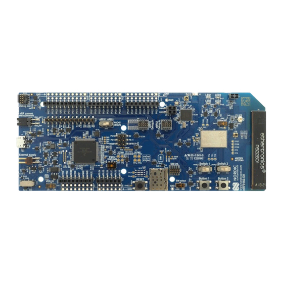
Page 13: Hardware Description
Hardware description The nRF9160 DK (PCA10090) features an onboard programming and debugging solution. 5.1 Hardware figures The nRF9160 DK hardware drawings show both sides of the PCA10090. Figure 5: nRF9160 DK (PCA10090), front view Figure 6: nRF9160 DK (PCA10090), back view 5.2 Block diagram... -
Page 14: Power Supply
Figure 7: nRF9160 DK block diagram 5.3 Power supply nRF9160 DK has a flexible and configurable power supply system to allow software development and testing using different power sources and to facilitate accurate power measurements. The power source options are: •... - Page 15 Hardware description Figure 9: Power sources and switches 4418_1216 v0.9.2...
-
Page 16: Nrf9160 Supply
Hardware description To ensure that only one of the power sources are used on the DK at a time, power switches are implemented on each of them as shown in Figure 9: Power sources and switches on page 15. These switches prioritize the supply sources in the following manner: 1. -
Page 17: Other Power Domains
This regulator also supplies the LEDs on the DK, giving these a fixed supply. 5.4 Antenna interfaces nRF9160 DK has three antenna interfaces mounted representing LTE, GPS, and the 2.4 GHz radio. The LTE and 2.4 GHz RF signals are propagated through two coaxial connectors with switches that will disconnect the corresponding antenna from the radio if adapter cables are connected. -
Page 18: Gpio Interfaces
Figure 12: GPS connected to the nRF9160 5.6 GPIO interfaces Access to the nRF9160 GPIOs is available from connectors P7, P10, P14, P19, and P27. The nRF9160 DK supports the Arduino UNO interface. 4418_1216 v0.9.2... - Page 19 GPIO signals are also available on connectors P5, P6, P12, P17, and P25, which are on the bottom side of the DK. By mounting pin lists on the connector footprints, the nRF9160 DK can be used as a shield for Arduino motherboards.
-
Page 20: Nrf52840
Hardware description Figure 14: nRF9160 DK pins 5.7 nRF52840 An nRF52840 Bluetooth/IEEE 802.15.4 System on Chip (SoC) is included on the nRF9160 DK. This device has two functions: • nRF9160 DK control • Bluetooth/IEEE 802.15.4 network processor Figure 15: nRF52840 SoC on the nRF9160 DK... -
Page 21: Nrf9160 Dk Board Control
Hardware description 5.7.1 nRF9160 DK board control The nRF52840 controls analog switches on the nRF9160 DK, enabling routing of some of the nRF9160 GPIO pins to onboard functionality, for example LEDs, or the regular GPIO interfaces. For details on which GPIOs on the nRF9160 can be routed by these analog switches, see the table below. -
Page 22: Bluetooth/Ieee 802.15.4 Network Processor
Note: To program and debug the nRF52840, nRF52 needs to be selected on the PROG/DEBUG switch (SW5). Since this firmware in the nRF52840 decides the nRF9160 DK behavior, it is vital that it is always present in the nRF52840. If it is accidentally erased or firmware affecting the use of the key nRF52840 GPIOs is programmed in, nRF9160 DK functionality is not guaranteed. -
Page 23: Buttons, Slide Switches, And Leds
Figure 16: nRF52840 board controller 5.8 Buttons, slide switches, and LEDs The nRF9160 DK has four LEDs, two buttons, and two switches for simple user interaction. By default, they are connected to nRF9160 GPIOs as shown in the following table. -
Page 24: Debug Input And Trace Options
5.9 Debug input and trace options The primary debug interface on the nRF9160 DK is the Segger OB debugger available through the USB port. However, if other than USB supply is used on the DK, this functionality will be disabled. -
Page 25: Debug Output
Table 6: nRF9160 trace interfaces 5.10 Debug output The nRF9160 DK supports programming and debugging external boards with Nordic SoCs and SiPs. To debug an external board with SEGGER J-Link OB IF, connect the Debug out connector P22 to your target board with a 10-pin flat cable. -
Page 26: Connectors For Programming External Boards
If the interface MCU detects target power on both P22 and P15, it will program/debug the target connected to P22 by default. If it is inconvenient to have a separate power supply on the external board, the nRF9160 DK can supply power through the Debug out connector P22. To enable this, short solder bridge SB37. -
Page 27: Signal Routing Switches
Hardware description Pin number Signal Description SWD0_SELECT Voltage supply from the external target, used as voltage detect input to the interface SWD0_SWDIO Serial Wire Debug (SWD) data line Ground SWD0_SWDCLK SWD clock line Ground SWD0_SWO Serial Wire Output (SWO) line N.C. -
Page 28: Switches For Uart Interface
Hardware description For more information, see Performance measurement mode on page 11. Figure 21: Signal interface switches 5.11.2 Switches for UART interface Two UART interfaces are routed between the interface MCU and the nRF9160 SiP. These can be controlled individually. 4418_1216 v0.9.2... -
Page 29: Switches For Buttons And Leds
Figure 22: UART interface switches 5.11.3 Switches for buttons and LEDs On the nRF9160 DK, there are a few analog switches that are used to connect and disconnect signals to control buttons, switches, and LEDs. The switches are controlled by the nRF52840, which contains firmware from Nordic Semiconductor. - Page 30 Hardware description Figure 23: LED switch control 4418_1216 v0.9.2...
-
Page 31: Switches For Nrf52840 Interface
Hardware description Figure 24: Buttons and switches, switch control 5.11.4 Switches for nRF52840 interface A total of three analog switches controls the routing of signals between the nRF9160 SiP and the nRF52840 SoC. There are a total of nine signals that can be routed between the devices, six GPIOs and three COEX pins. -
Page 32: Sim And Esim
5.12 SIM and eSIM The nRF9160 DK is designed to support both regular and embedded SIM (eSIM). For this purpose, it has a pluggable SIM card socket that takes a nano-sized SIM (4FF) and a non-populated footprint for an eSIM (MFF2). -
Page 33: Additional Interfaces
MAGPIO pins. On the nRF9160 DK, MAGPIO0 is used to enable the GPS LNA, while the remaining two MAGPIOs are not in use in this DK. The user can access MAGPIO0, MAGPIO1, and MAGPIO2 through test points TP58, TP2, and TP3. -
Page 34: Sip Enable
DK) and pull the pin low. 5.15 Solder bridge configuration The nRF9160 DK has a range of solder bridges for enabling or disabling functionality on the DK. Changes to these are not needed for normal use of the DK. - Page 35 Hardware description Solder bridge Default Function SB28 Open Short to connect the RESET pin on the Arduino interface to the nRF9160 reset pin SB29 Open Short to connect the RESET pin on the Arduino interface to the nRF9160 reset pin when the interface MCU is disconnected SB30 Open Short to connect the RESET pin on the Arduino interface to the...
-
Page 36: Measuring Current
Measuring current The current drawn by the nRF9160 can be monitored on the nRF9160 DK. Current can be measured using various test instruments. Examples of test equipment are the following: • Power analyzer • Oscilloscope • Ampere-meter Connector P24 can be used for measuring current consumption or monitoring voltage levels to the nRF9160. -
Page 37: Using An Oscilloscope For Current Profile Measurement
Measuring current Figure 29: nRF power source 6.2 Using an oscilloscope for current profile measurement An oscilloscope can be used to measure the current over a given or continuous time interval and to capture the current profile. Before you start, make sure you have prepared the DK as described in section Preparing the development kit for current measurements on page 36. - Page 38 Measuring current Figure 31: Current measurement with a current meter Note: Use a high-speed, high-dynamic-range ampere meter for the best and most reliable measurements. Current range switching in the current meter may affect the power supply to the nRF9160. High speed and bandwidth is required to detect rapid changes in the current consumption in the nRF9160.
-
Page 39: Rf Measurements
RF measurements The nRF9160 DK is equipped with a small size coaxial connectors J1 and J7 for measuring the RF signal for LTE and 2.4 GHz. The connectors are of SWF type (Murata part no. MM8130-2600) with an internal switch. By default, when no cable is attached, the RF signal is routed to the onboard antenna. -
Page 40: Radiated Performance Of Nrf9160 Dk
73.8 Table 10: Antenna performance versus radio band The 2.4 GHz antenna on the nRF9160 DK is optimized for the frequency range of 2.4–2.48 GHz. It has an average return loss of -15 dB, average efficiency being 80 %. 4418_1216 v0.9.2... -
Page 41: Glossary
Glossary Band-Pass Filter (BPF) An electronic device or circuit that passes frequencies within a certain range and rejects frequencies outside that range. Cat-M1 LTE-M User Equipment (UE) category with a single RX antenna, specified in 3GPP Release 13. Cat-NB1 Narrowband Internet of Things (NB-IoT) User Equipment (UE) category with 200 kHz UE bandwidth and a single RX antenna, specified in 3GPP Release 13. - Page 42 Receive Data (RXD) A signal line in a serial interface that receives data from another device. Request to Send (RTS) In flow control, the transmitting end is ready and requesting the far end for a permission to transfer data. SAW filter A high-performing filter using Surface Acoustic Wave (SAW) technology.
-
Page 43: Acronyms And Abbreviations
Acronyms and abbreviations These acronyms and abbreviations are used in this document. Band-Pass Filter Clear to Send Development Kit FIDO Fast Identity Online Global Positioning System HWFC Hardware Flow Control Inter-integrated Circuit Low-Dropout (Regulator) Low-Noise Amplifier Request to Send Receive Data Surface Acoustic Wave System in Package System on Chip... -
Page 44: Legal Notices
Nordic Semiconductor ASA customers using or selling these products for use in such applications do so at their own risk and agree to fully indemnify Nordic Semiconductor ASA for any damages resulting from such improper use or sale.
Need help?
Do you have a question about the nRF9160 DK and is the answer not in the manual?
Questions and answers