
Related Manuals for Cypress PSoC 1 CY3210-PSoCEVAL1


Summary of Contents for Cypress PSoC 1 CY3210-PSoCEVAL1
- Page 1 CY3210-PSoCEVAL1 ® PSoC 1 Evaluation Kit Guide Doc. #: 001-66768 Rev. *F Cypress Semiconductor 198 Champion Court San Jose, CA 95134-1709 www.cypress.com...
- Page 2 A critical component is any component of a device or system whose failure to perform can be reasonably expected to cause the failure of the device or system, or to affect its safety or effectiveness. Cypress is not liable, in whole or in part, and you shall and hereby do release Cypress from any claim, damage, or other liability arising from or related to all Unintended Uses of Cypress products.
-
Page 3: Table Of Contents
Contents 1. Introduction Kit Contents .........................5 Additional Learning Resources..................6 1.2.1 PSoC Designer ....................7 1.2.2 Code Examples....................8 1.2.3 PSoC Designer Help ..................10 1.2.4 Technical Support...................10 Documentation Conventions..................12 2. Getting Started Kit Installation ......................13 PSoC Designer ......................17 PSoC Programmer ....................18 3. Kit Operation Evaluating the PSoC 1 Device...................19 3.1.1 Programming Specifications and Connections ..........20 4. - Page 4 Contents 5.3.1 Project Description ..................55 5.3.2 Hardware Connections...................56 5.3.3 Code Example 3 Flowchart ................56 5.3.4 Verifying Output....................57 Code Example 4: ASM_Example_DAC_ADC ............57 5.4.1 Project Description ..................57 5.4.2 Hardware Connections...................59 5.4.3 Code Example 4 Flowchart ................59 5.4.4 Verifying Output....................60 Code Example 5: ASM_Example_Dynamic_PWM_PRS ..........61 5.5.1 Project Description ..................61 5.5.2 Hardware Connections...................63 5.5.3 Code Example 5 Flowchart ................64...
-
Page 5: Introduction
■ LCD module ■ Single strand jumper wire pack ■ Inspect the contents of the kit; if any parts are missing, contact your nearest Cypress sales office for help. CY3210-PSoCEVAL1 PSoC® 1 Evaluation Kit Guide, Doc. #: 001-66768 Rev. *F... -
Page 6: Additional Learning Resources
■ In addition, PSoC Designer includes a device selection tool. ■ Application notes: Cypress offers a large number of PSoC application notes covering a broad ■ range of topics, from basic to advanced level. Recommended application notes for getting started with PSoC 1 are: ®... -
Page 7: Psoc Designer
Introduction 1.2.1 PSoC Designer PSoC Designer is a free Windows-based Integrated Design Environment (IDE). Develop your applications using a library of pre-characterized analog and digital peripherals in a drag-and-drop design environment. Then, customize your design leveraging the dynamically generated API libraries of code. -
Page 8: Code Examples
PSoC Designer User modules can be used for various applications. http://www.cypress.com/go/PSoC1Code Examples. To access the Code Examples integrated with PSoC Designer, follow the path Start Page > Design Catalog >... - Page 9 Introduction In the Example Projects Browser shown in Figure 1-3, you have the following options. Keyword search to filter the projects. ■ Listing the projects based on Category. ■ Review the datasheet for the selection (on the Description tab). ■ Review the code example for the selection.
-
Page 10: Psoc Designer Help
If you have any questions, our technical support team is happy to assist you. You can create a support request on the Cypress Technical Support page. If you are in the United States, you can talk to our technical support team by calling our toll-free number: +1-800-541-4736. - Page 11 Introduction Visit http://www.cypress.com for additional learning resources in the form of datasheets, technical reference manual, and application notes. For the latest information about this kit, visit http://www.cypress.com/go/CY3210-PSoCEval1. PSoC Designer: PSoC Designer Overview ■ http://www.cypress.com/go/psocdesigner PSoC Designer Training: PSoC Designer On-Demand Training Series and Videos ■...
-
Page 12: Documentation Conventions
Introduction Documentation Conventions Table 1-1. Document Conventions for Guides Convention Usage Displays file locations, user entered text, and source code: Courier New C:\ ...cd\icc\ Displays file names and reference documentation: Italics Read about the sourcefile.hex file in the PSoC Designer User Guide. Displays keyboard commands in procedures: [Bracketed, Bold] [Enter] or [Ctrl] [C]... -
Page 13: Getting Started
Note You can also download the latest kit installer from http://www.cypress.com/go/CY3210- PSoCEval1. Three different types of installers are available for download. a. CY3210-PSoCEval1_ISO: This file (ISO image) is an archive file of the optical disc provided with the kit. - Page 14 Getting Started Note If auto-run does not execute, double-click cyautorun.exe file on the root directory of the DVD, as shown in Figure 2-2. To access the root directory, click Start > My Computer > CY3210- PSoCEVAL1 <drive:>. Figure 2-2. Root Directory of DVD 3.
- Page 15 Getting Started Figure 2-4. Installation Type Options 8. When the installation begins, a list of all packages appear on the Installation Page. A green check mark appears against every package that is downloaded and installed, as shown in Figure 2-5. 9.
- Page 16 Getting Started 10.Click Finish to complete the installation. Figure 2-6. Installation Complete After software installation, drivers are installed when MiniProg1 is connected to the PC for the first time. Verify driver installation by opening PSoC Programmer with the MiniProg connected to the USB port of the PC.
-
Page 17: Psoc Designer
This section gives a brief introduction on the PSoC Designer Interconnect View. Additional details on the PSoC Designer software is given in the Code Examples chapter on page 1. Click Start > All Programs > Cypress > PSoC Designer <version> > PSoC Designer <ver- sion>. Figure 2-7. PSoC Designer Interconnect View Note The Datasheet and Resource Meter windows are hidden by default. -
Page 18: Psoc Programmer
This section gives a brief introduction on programming PSoC; for kit specific programming instruc- tion, see Programming Specifications and Connections on page 1. Click Start > All Programs > Cypress > PSoC Programmer <version> > PSoC Programmer <version>. 2. Select the MiniProg from Port Selection. -
Page 19: Kit Operation
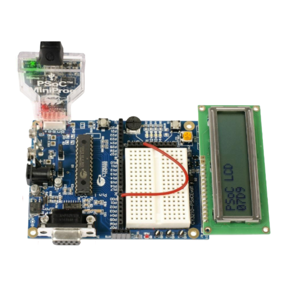
Kit Operation The CY3210-PSoCEVAL1 kit helps in evaluating applications using the PSoC 1 family of devices. This kit can be used to work with the different user modules provided in the PSoC Designer software and explore hardware features that are integrated into the PSoC 1 device. Evaluating the PSoC 1 Device The CY3210-PSoCEVAL1 board is populated with a preprogrammed CY8C29466-24PXI part. -
Page 20: Programming Specifications And Connections
Kit Operation Figure 3-1. PSoCEVAL1 Evaluation Board 3.1.1 Programming Specifications and Connections When the MiniProg is connected, you can use PSoC Programmer to program the CY3210- PSoCEVAL1 Evaluation kit. Plug in the USB cable into the MiniProg before attaching it to the ISSP header on the board. - Page 21 Kit Operation Figure 3-2. Programming PSoC Device Figure 3-3. PSoC Programmer Screen CY3210-PSoCEVAL1 PSoC® 1 Evaluation Kit Guide, Doc. #: 001-66768 Rev. *F...
- Page 22 4. Open PSoC Programmer. 5. Click the Load File button and browse to the hex file location (<Install_direc- tory>:\Cypress\CY3210-PSoCEVAL1\<version>\Firmware\ ASM_Example_AD- C_UART_LCD\ASM_Example_ADC_UART_LCD.hex). Click Open to select the hex file. 6. Click Connect or double-click on the respective MiniProg under Port Selection to select or con- nect to MiniProg.
-
Page 23: Hardware
Hardware This section provides an overview of the development kit hardware, including power system, jumper setting, and programming interface. To start using the board, go to “Code Examples” on page CY3210-PSoCEVAL1 System Block Diagram The CY3210-PSoCEVAL1 Evaluation Kit consists of: Power supply system ■... -
Page 24: Functional Description
Hardware Functional Description The CY3210-PSoCEVAL1 Evaluation Kit demonstrates the function of PSoC 1 devices. Connect the device to onboard peripherals such as potentiometer, LEDs, LCD, and RS-232. The board also has additional features such as a general prototype area (bread board) and an ISSP programming header. - Page 25 Hardware Figure 4-3. Power Supply Schematic 9-V Battery Connector 9-V to 12-V 1-Amp Input Install Jumper for 3.3-V Operation and Remove Jumper for 5-V Operation 4.2.1.1 Protection Circuit A reverse-voltage and over-voltage protection circuit is added at the expansion port on VCC lines. The protection circuit consists of two P-channel MOSFETs on the power line allowing the power/cur- rent to flow from input to output depending on the voltages applied at the external board connector.
- Page 26 Hardware 4.2.1.2 Jumper Settings Figure 4-5. Jumper Settings The functions of JP1, JP2, and JP3 are as follows: JP1 connects P16 to Rx pin for UART communication and should be removed for normal I/O ■ operation. JP2 connects P27 to Tx pin for UART communication and should be removed for normal I/O ■...
-
Page 27: Programming Interface
Hardware 4.2.2 Programming Interface This kit allows programming of the PSoC device via the ISSP programming header using a MiniProg. Figure 4-6. Programming Interface Schematic 4.2.3 PSoC 1 Parts Two parts are available with the CY3210-PSoCEVAL1 Evaluation Kit. PSoC CY8C29466-24PXI 28-Pin DIP ■... -
Page 28: Rs-232 Interface
Hardware Table 4-1. Pin Description (continued) Description Connected To Name P1[3] J8.4 J8.2 and XTAL /Sclk P1[1] Crystal (XTALin), I C Serial Clock (SCL), ISSP-SCLK Ground connection J8.1 and XTAL P1[0] Crystal (XTALout), I C Serial Data (SDA), ISSP-SDATA Sdata P1[2] J8.3 P1[4]... -
Page 29: Prototyping Area
Hardware 4.2.5 Prototyping Area The prototyping area has three complete ports for custom circuit development: port 0, port 1, and port 2. These ports can be used with the prototyping area to create simple yet elegant analog designs. Figure 4-8. Prototyping Area Schematic There are power and ground connections close to the prototyping area for convenience. -
Page 30: Character Lcd Interface
Hardware Figure 4-9. Prototyping Area Schematic 4.2.6 Character LCD Interface The kit has a character 2×16 alphanumeric LCD module, which goes into the character LCD header, J9. The LCD runs on a 5-V supply and can function regardless of the voltage on which PSoC is powered. -
Page 31: Code Examples
Code Examples Six code examples are included in the following sections. All code examples are available on the CY3210-PSoCEVAL1 kit DVD or at this location: <Install_directory>:\Cypress\ CY3210-PSoCEVAL1\<version>\Firmware . My First Code Example 5.1.1 Project Description This project demonstrates a 12-bit incremental ADC by measuring the voltage of the potentiometer, transmitting the conversion result on the UART, and displaying it on the LCD. - Page 32 Code Examples Figure 5-1. New Project Window 5. To select the target device, click Device Catalog , as shown in Figure 5-2. Figure 5-2. Select Device Catalog 6. The Device Catalog window opens. Select CY8C29466-24PXI from the list and click Create Project with 'CY8C29466-24PXI' .
- Page 33 Code Examples Figure 5-3. Device Catalog Window 7. In the Generate 'Main' File Using: option, select C and click OK . 8. By default, the project opens in Chip view, as shown in Figure 5-4. CY3210-PSoCEVAL1 PSoC® 1 Evaluation Kit Guide, Doc. #: 001-66768 Rev. *F...
- Page 34 Code Examples Figure 5-4. Default View 9. Configure the modules required for this design. Also, connect the modules together and to the pins on the PSoC. In the User Modules section, expand the ADCs folder. Figure 5-5. User Modules Window 10.In this folder, right-click on ADCINC and select Place .
- Page 35 Code Examples Figure 5-6. Multi User Module The user module (UM) is placed in the first available analog block. By default, the UM is placed on an Analog Switched Capacitor Type C block. It should be shifted to a Switched Capacitor Type D block, as explained in the next step.
- Page 36 Code Examples Figure 5-8. ADCINC User Module Placement 12.Configure the ADCINC_1 properties, as shown in Figure 5-9. Figure 5-9. ADCINC User Module Properties 13.In the User Modules window, expand the Amplifiers folder and double-click on PGA to place a programmable gain amplifier (PGA) in the design. 14.By default, the PGA is placed on the ACB00 analog block.
- Page 37 Code Examples Figure 5-10. PGA User Module Placement 15.Configure the PGA properties, as shown in Figure 5-11. Figure 5-11. PGA User Module Properties 16.Click on AnalogColumn_InputSelect_1 multiplexer in the Design window and change the input multiplexer to AnalogColumn_InputMUX_0. The analog input from P0[1] is routed to the ADC module through a PGA at unity gain (Gain is a configurable parameter in the PGA module).
- Page 38 Code Examples Figure 5-12. Connecting PGA to Port Pin 17.In the User Modules window, expand the Misc Digital folder and double-click on LCD to place an LCD in the design. Configure the properties of the LCD UM. Enable the BarGraph property to include additional APIs into the project and allow the bar graph display on the LCD.
- Page 39 Code Examples Figure 5-14. LCD User Module Placement 18.In the User Modules window, expand the Digital Comm folder and double-click on UART to place a UART in the design. Configure the properties of the UART UM, as shown in Figure 5-15.
- Page 40 Code Examples Figure 5-16. Auto Routing b. Manual Routing: Configure the look-up table (LUT) on Row_0_Input2 to GlobalOddEven bus. To do so, click on the Row_0_Input_2 bus to open the Digital Interconnect window. Figure 5-17. Digital InterConnect Window 20.Click on Row_0_Input_2 demultiplexer in the Interconnect window and select GlobalInOdd_6 ; click Close .
- Page 41 Code Examples Figure 5-18. Configure Row_0_Input_2 to GlobalInOdd_6 21.Click on GlobalInOdd_6 . Select Port_1_6 from the drop-down list in the Pin field; click OK . Figure 5-19. Pin Select Figure 5-20. Pin Select 22.Route the TX signal of UART to P2[7]. There are two methods to do this: a.
- Page 42 Code Examples Figure 5-21. Auto-Routing b. Manual Routing: Configure the LUT on Row_0_Output3. To do so, click on Row_0_Output3 to open the Digital Interconnect window. 23.In this window, enable Row_0_Output_3_Drive_1 to connect to GlobalOutEven_7. Figure 5-22. Digital InterConnect Window 24.Click Close . CY3210-PSoCEVAL1 PSoC®...
- Page 43 Code Examples 25.Click on GlobalOutEven_7 . Select Port_2_7 from the drop-down list in the Pin field; click OK . Figure 5-23. Pin Select Figure 5-24. Pin Select 26.Configure the Global Resources window to match the following figure. CY3210-PSoCEVAL1 PSoC® 1 Evaluation Kit Guide, Doc. #: 001-66768 Rev. *F...
- Page 44 Code Examples Figure 5-25. Global Resources Window Note a. The clock divider VC1 provides a 3-MHz sample clock to the ADCINC, resulting in a sample rate of 180 samples per second. b. The clock divider VC3 generates the baud clock for UART by dividing 24 MHz by 156. The UART internally divides UART clock (VC3 in this example) by 8, resulting in a baud rate of 19200 bits per second.
- Page 45 Code Examples 28.Save the project. 29.To build the project, click Build > Generate/Build 'Example_My_First_PSoC_Project' . 30.Connect the CY3210 PSoCEVAL1 board to a PC through a MiniProg1. Figure 5-27. Connect MiniProg1 to Board The board can be programmed either through PSoC Designer IDE or by launching PSoC Pro- grammer.
-
Page 46: Verifying Output Using Lcd
Code Examples b. In the Program Part window, configure the following settings: Port Selection: Select MiniProg1/xxxxxxxxxxx and then Connected Acquire Mode: Power Cycle Verification: Off Power Settings: 5.0 V c. Click on the Program button (see Figure 5-28) to start programming the board. d. -
Page 47: Verifying Output Using Uart
Code Examples Note The measured value might have an error of upto 10 counts due to ADC offset or potentiom- eter inaccuracy. Figure 5-31. LCD Displaying ADC Value 4. Vary the potentiometer and observe the change in the value of LCD. Note ADC values may fluctuate several counts due to system noise or if the potentiometer volt- age is at the edge of an ADC count. - Page 48 Code Examples Figure 5-32. CY3210-PSoCEVAL1 Connected to RS-232 Cable 1. Connect the hardware as explained in “Verifying Output using LCD” on page 46 section. 2. Open a terminal application such as HyperTerminal or TeraTerm with these parameters: a. Baud Rate: 19200 b.
- Page 49 Code Examples 3. Power the board by clicking on the Toggle Power button in the Program Part window 4. The ADC value is displayed on the HyperTerminal and on the LCD, as shown in Figure 5-34 Figure 5-35 Figure 5-34. Verify Output on LCD Figure 5-35.
-
Page 50: Code Example 2: Asm_Example_Adc_Uart_Lcd
5.1.2 Creating My First PSoC 1 Project. 4. Open the existing main.asm file in Workspace Explorer. Replace the existing main.asm content with the content from the file located at <Install_directory>:\Cypress\CY3210-PSo- CEVAL1\<version>\Firmware\ASM_Example_ADC_UART_LCD\ ASM_Example_AD- C_UART_LCD\main.asm . 5. Follow steps 30 through 32 from 5.1.2 Creating My First PSoC 1 Project... -
Page 51: Hardware Connections
Code Examples Figure 5-36. Device Configuration for ADC Conversion and LCD Display 5.2.3 Hardware Connections ADC input (0–Vdd): Connect P01 to VR ■ Serial Rx: Place jumper (shunt) on JP1 to connect P16 and Rx ■ Serial Tx: Place jumper (shunt) on JP2 to connect P27 and Tx ■... -
Page 52: Code Example 2 Flowchart
Code Examples Figure 5-37. Hardware Connection: Code Example 2 5.2.4 Code Example 2 Flowchart Start Initialize UART, PGA, ADC, LCD Enable Global Interrupts ADC Converted Data Available? Read Result, Clear Flag Print Result to UART Display Results in HEX on LCD CY3210-PSoCEVAL1 PSoC®... -
Page 53: Verifying Output Using Lcd
Code Examples 5.2.5 Verifying Output using LCD When the example code is built and programmed into the device, reset the device by pressing the RESET button or power cycling the board. The voltage of the potentiometer is measured by the ADC and is output as a four-digit hex value on the LCD. - Page 54 Code Examples Figure 5-40. Verify Output on HyperTerminal CY3210-PSoCEVAL1 PSoC® 1 Evaluation Kit Guide, Doc. #: 001-66768 Rev. *F...
-
Page 55: Code Example 3: Asm_Example_Blink_Led
Code Examples Code Example 3: ASM_Example_Blink_LED 5.3.1 Project Description This project demonstrates how an LED blinks at a constant duty cycle using a hardware PWM. PWM8: The clock dividers VC1, VC2, and VC3 are used to divide the 24-MHz system clock by 16, 16, and 256, respectively. -
Page 56: Hardware Connections
Code Examples 5.3.2 Hardware Connections Connect P20 to LED1. ■ Figure 5-42. Hardware Connection: Code Example 3 5.3.3 Code Example 3 Flowchart Start PWM, Enable PWM Interrupt Enable Global Interrupt Blink LED CY3210-PSoCEVAL1 PSoC® 1 Evaluation Kit Guide, Doc. #: 001-66768 Rev. *F... -
Page 57: Verifying Output
Code Examples 5.3.4 Verifying Output When the example code is built and programmed into the device, make all the hardware connections and reset the board by pressing the RESET button or by power cycling the board. The LED1 blinks with a blink period of 1.4 Hz. Note Remove the jumper JP3 to verify output at 5 V. - Page 58 Code Examples Figure 5-44. Device Configuration to Output a Sine Wave CY3210-PSoCEVAL1 PSoC® 1 Evaluation Kit Guide, Doc. #: 001-66768 Rev. *F...
-
Page 59: Hardware Connections
Code Examples 5.4.2 Hardware Connections ADC Input (0–Vdd): Connect P01 to VR ■ DAC Output (0–Vdd): Connect P05 to LED1 and CRO ■ Figure 5-45. Hardware Connections: Code Example 4 5.4.3 Code Example 4 Flowchart Start ADC Value Update Counter Turn on PGA, Start DAC Enable Global Interrupts... -
Page 60: Verifying Output
Code Examples 5.4.4 Verifying Output After the example code is built and programmed into the device, make all the hardware connections and reset the board by pressing the RESET button or by power cycling the board. LED1 is a sine wave output whose period is based on the ADC. -
Page 61: Code Example 5: Asm_Example_Dynamic_Pwm_Prs
Code Examples Code Example 5: ASM_Example_Dynamic_PWM_PRS 5.5.1 Project Description This project demonstrates the Dynamic Reconfiguration capability of PSoC Designer. A set of user modules is called a configuration. A loadable configuration consists of one or more UMs placed with module parameters, global resources, pinouts, and generated application files. The UMs used and the register settings can be changed easily. - Page 62 Code Examples When the SW switch is pressed, the PWM configuration is unloaded and the PRS configuration is loaded. In this configuration, LED1 and LED3 are used to output the PRS Pulse Density and PRS Bitstream, respectively. The APIs UnloadConfig_<configname> and LoadConfig_<configname> are used to unload and load the required configurations Counter8: In the base configuration, it takes a clock of 732 Hz as an input.
-
Page 63: Hardware Connections
Code Examples Figure 5-49. PWM Configuration Figure 5-50. PRS Configuration 5.5.2 Hardware Connections User button: Connect P14 to SW ■ PWM pulse width or PRS pulse density: Connect P20 to LED1 ■ PWM terminal count: Connect P22 to LED2 ■ PRS bitstream: Connect P23 to LED3 ■... -
Page 64: Code Example 5 Flowchart
Code Examples Figure 5-51. Hardware Connection: Code Example 5 5.5.3 Code Example 5 Flowchart Start Clock Generator, Load PRS Configuration Update PRS Configuration, Load PWM Configuration Start PWM Button Pressed? Unload PWM Configuration, Load PRS Configuration Start PRS, Load Compared Value Button Released CY3210-PSoCEVAL1 PSoC®... -
Page 65: Verifying Output
Code Examples 5.5.4 Verifying Output Program the board with the hex file; disconnect power and make all hardware connections. Remove the LCD module and power the board. When the switch is released, the PWM configuration is loaded and LED1 and LED2 blink with PWM Pulse Width and PWM Terminal Count, respectively. When the switch is pressed, the PRS configuration is loaded and LED1 and LED3 blinks with PRS Pulse Density and PRS Bitstream, respectively. -
Page 66: Code Example 6: Asm_Example_Led_Logic
Code Examples Code Example 6: ASM_Example_LED_Logic 5.6.1 Project Description This project demonstrates a PSoC project designed to blink an LED using the output of two PWMs. The outputs are combined using an AND gate in an output bus logic block. This logical combination results in a beat frequency of 1.4 Hz. -
Page 67: Hardware Connections
Code Examples 5.6.2 Hardware Connections Connect P20 to LED1 ■ Figure 5-54. Hardware Connection: Code Example 6 5.6.3 Code Example 6 Flowchart Enable PWM1 and PWM2 Blink LED 5.6.4 Verifying Output After the program is built and programmed into the device, make all the hardware connections and reset the board by either pressing the RESET button or by power cycling the board. - Page 68 Code Examples Figure 5-55. Verify Output: Code Example 6 “Replace CY8C29466-24PXI with CY8C27443-24PXI” on page 74 for instructions on how to replace the CY8C29466-24PXI PSoC part with CY8C27443-24PXI. CY3210-PSoCEVAL1 PSoC® 1 Evaluation Kit Guide, Doc. #: 001-66768 Rev. *F...
-
Page 69: Appendix
Appendix The schematic and board layouts are available on the CY3210-PSoCEVAL1 kit DVD or at this location: <Install_directory>:\Cypress\CY3210-PSoCEVAL1\<version>\Hardware. Schematic A.1.1 CY3210-PSoCEVAL1 Board Schematic VCC_EXT 0.1uF,16V 10uF,16V Vout 0.47uF,16V PMOS( DMP3098L-7) 0.1uF,16V 22uF,10V 10uF,16V PMOS( DMP3098L-7) 220ohm R1out R1in R2out R2in... -
Page 70: Board Layout
Appendix Board Layout Figure A-1. Top Copper Layer CY3210-PSoCEVAL1 PSoC® 1 Evaluation Kit Guide, Doc. #: 001-66768 Rev. *F... - Page 71 Appendix Figure A-2. Bottom Copper Layer CY3210-PSoCEVAL1 PSoC® 1 Evaluation Kit Guide, Doc. #: 001-66768 Rev. *F...
- Page 72 Appendix Figure A-3. Top Overlay CY3210-PSoCEVAL1 PSoC® 1 Evaluation Kit Guide, Doc. #: 001-66768 Rev. *F...
-
Page 73: Bill Of Materials
Appendix Bill of Materials Item Qty Reference Value Description Manufacturer Manufacturer Part No. rev *B PDC-9286 PSoC EVAL1 Board Cypress PDC-9286 C1, C3, C6 0.1uF,16V Capacitor YAGEO (PHYCOMP) CC0805ZRY5V9BB104 C2, C4, C5 0.47uF,16V Capacitor MULTICOMP MCCA000287 22uF,10V Capacitor NICHICON UWX1A220MCL1GB... -
Page 74: Replace Cy8C29466-24Pxi With Cy8C27443-24Pxi
Appendix Replace CY8C29466-24PXI with CY8C27443-24PXI The CY3210-PSoCEVAL1 kit includes two PSoC parts, CY8C29466-24PXI and CY8C27443-24PXI. The CY8C29466-24PXI part is placed on the IC socket of the board when shipped. To replace the default part with CY8C27443-24PXI, follow these instructions. Use an IC extractor – place the ends of the extractor between the IC and the socket. Gently pull the IC out evenly, away from the board. - Page 75 Appendix Figure A-6. Place New Chip CY3210-PSoCEVAL1 PSoC® 1 Evaluation Kit Guide, Doc. #: 001-66768 Rev. *F...
-
Page 76: Revision History
“PSoC Designer” on page Added “Code Examples” on page Added “PSoC Designer Help” on page Added “Technical Support” on page 5753924 09/01/2017 NIBK Updated Cypress Logo and Copyright. Distribution: External Posting: None CY3210-PSoCEVAL1 PSoC® 1 Evaluation Kit Guide, Doc. #: 001-66768 Rev. *F...
Need help?
Do you have a question about the PSoC 1 CY3210-PSoCEVAL1 and is the answer not in the manual?
Questions and answers