Table of Contents
Advertisement
SERVICE MANUAL
Ver. 1.1 2008.08
• HCD-F200 is the DVD system, USB, tuner and video section
in DAV-F200.
• HCD-F500 is the DVD system, USB, tuner and video section
in DAV-F500.
Note:
• In this set, repair in the state of having connected with SA-
WSF200.
• In this set, repair in the state of having connected with SA-
WSF500.
This product incorporates copyright protection technology that is
protected by U.S. patents and other intellectual property rights.
Use of this copyright protection technology must be authorized by
Macrovision, and is intended for home and other limited viewing
uses only unless otherwise authorized by Macrovision. Reverse
engineering or disassembly is prohibited.
This system incorporates with Dolby* Digital and Dolby Pro Log-
ic (II) adaptive matrix surround decoder and the DTS** Digital
Surround System.
* Manufactured under license from Dolby Laboratories.
Dolby, Pro Logic, and the double-D symbol are trademarks of
Dolby Laboratories.
** Manufactured under license under U.S. Patent #'s: 5,451,942;
5,956,674; 5,974,380; 5,978,762; 6,487,535 & other U.S. and
worldwide patents issued & pending. DTS and DTS Digital
Surround are registered trademarks and the DTS logos and
Symbol are trademarks of DTS, Inc. © 1996-2007 DTS, Inc.
All Rights Reserved.
This system incorporates High-Defi nition Multimedia Interface
(HDMITM) technology.
HDMI, the HDMI logo and High-Defi nition Multimedia Interface
are trademarks or registered trademarks of HDMI Licensing LLC.
"BRAVIA" is a trademark of Sony Corporation.
"S-AIR" and its logo are trademarks of Sony Corporation.
Sony Corporation
9-889-150-02
2008H05-1
Audio&Video Business Group
©
2008.08
Published by Sony Techno Create Corporation
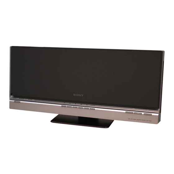
HCD-F200/F500
Photo: HCD-F500
Model Name Using Similar Mechanism
DVD Mechanism Type
Optical Pick-up Block Name
Inputs (Analog)
TV (AUDIO IN)
Sensitivity: 450/250 mV
Inputs (Digital)
SAT/CABLE (COAXIAL)
Impedance: 75 ohms
Output (Digital) (HCD-F200)
Impedance: 75 ohms
DVD System
Laser
Semiconductor laser
(DVD: λ = 650 nm)
(CD: λ = 790 nm)
Emission duration: continuous
Signal format system
Canadian and Latin American models:
NTSC
Other models:
NTSC/PAL
USB Section
Supported bit rate
MP3 (MPEG 1 Audio Layer-3):
32 kbps - 320 kbps
WMA:
48 kbps - 192 kbps
AAC:
48 kbps - 320 kbps
Sampling frequencies
MP3 (MPEG 1 Audio Layer-3):
32/44.1/48 kHz
WMA:
44.1 kHz
AAC:
44.1 kHz
(USB) port:
Maximum current: 500 mA
Canadian Model
Australian Model
Russian Model
Singapore Model
SPECIFICATIONS
Tuner Section
System
FM tuner section
Tuning range
Canadian models:
Other models:
Antenna (aerial)
Antenna (aerial) terminals
Intermediate frequency 10.7 MHz
Video Section
Outputs
– Continued on next page –
DVD RECEIVER
E Model
HCD-F500
AEP Model
UK Model
HCD-F200
Thai Model
HCD-F200/F500
NEW
CDM86-DVBU101
KHM-313CAB
PLL quartz-locked digital
synthesizer
87.5 MHz - 108.0 MHz
(100 kHz step)
87.5 MHz - 108.0 MHz
(50 kHz step)
FM wire antenna (aerial)
75 ohms, unbalanced
VIDEO: 1 Vp-p 75 ohms
COMPONENT:
Y: 1 Vp-p 75 ohms
P
/C
, P
/C
: 0.7 Vp-p
B
B
R
R
75 ohms
HDMI OUT: Type A
(19 pin)
Advertisement
Table of Contents

Subscribe to Our Youtube Channel
Related Manuals for Sony HCD-F200


Summary of Contents for Sony HCD-F200
- Page 1 HCD-F200 Singapore Model Thai Model HCD-F200/F500 Photo: HCD-F500 • HCD-F200 is the DVD system, USB, tuner and video section Model Name Using Similar Mechanism in DAV-F200. DVD Mechanism Type CDM86-DVBU101 • HCD-F500 is the DVD system, USB, tuner and video section in DAV-F500.
- Page 2 LES DIAGRAMMES SCHÉMATIQUES ET LA LISTE DES PIÈCES SONT CRITIQUES POUR LA SÉCURITÉ DE FONC- TIONNEMENT. NE REMPLACER CES COMPOSANTS QUE PAR DES PIÈCES SONY DONT LES NUMÉROS SONT DON- NÉS DANS CE MANUEL OU DANS LES SUPPLÉMENTS PUBLIÉS PAR SONY.
-
Page 3: Table Of Contents
HCD-F200/F500 TABLE OF CONTENTS SERVICING NOTES EXPLODED VIEWS ..........7-1. Rear Cover Section ............58 GENERAL 7-2. Front Panel Section ............59 ..............7-3. Main Section ..............60 7-4. Chassis Section ............... 61 DISASSEMBLY 7-5. DVD Mechanism Deck Section-1 3-1. Disassembly Flow ............10 (CDM86-DVBU101) ............ -
Page 4: Servicing Notes
It is best to use only unleaded solder but unleaded solder may Part No. also be added to ordinary solder. BEGIN IT BEFORE THE REPAIR (HCD-F200) When the HCD-F200 is checked, connect to SA-WSF200 (for ac- tive speaker of DAV-F200). Be sure in advance the SA-WSF200 is prepared. Model Part No. - Page 5 HCD-F200/F500 Note on DualDiscs Playable Discs A DualDisc is a two sided disc product which mates DVD recorded material on one side with digital audio material on the other side. However, since the audio material side does not conform to the Compact Disc (CD) standard, playback on this product is not guaranteed.
- Page 6 HCD-F200/F500 PRECAUTION WHEN REMOVING OPTICAL PICK-UP BLOCK OR DMB-FIT BOARD CAUTION Be sure to execute a solder bridge as a measure against static electricity when removing the OP block (DVBU101) or DMB-FIT board. (Otherwise, the OP block will be destroyed.) Lift up the FFC holder.
- Page 7 HCD-F200/F500 MAIN BOARD SERVICE POSITION • In checking the MAIN board, prepare extension jig (Part No. J-2501-243-A: 1.00 mm pitch, 17 cores, length 300 mm). Note: Pleaese connect it afrer taking out MAIN board, DMB-FIT board and DVD mechanism block of the set referring to Section 3 Disassembly...
-
Page 8: General
HCD-F200/F500 SECTION 2 This section is extracted GENERAL from instruction manual. Control unit HCD-F200 Connector panel Top view Front view Right side view Left side view AUTO WIDE STAGE FUNCTION Ventilation slots Remote sensor VOL +/– buttons (on/standby) button ANTENNA (FM75... - Page 9 HCD-F200/F500 Front panel display Remote control HCD-F200 HCD-F200 ALPHABETICAL ORDER BUTTON DESCRIPTIONS A – L M – Z ANALOG MENU/HOME Number buttons SLEEP MUTING TUNED TITLE CHAP STEREO MONO NTSC NIGHT ANGLE MUTING (on/standby) REPEAT 1 AUDIO NIGHT TV /...
-
Page 10: Disassembly
HCD-F200/F500 SECTION 3 DISASSEMBLY • This set can be disassembled in the order shown below. 3-1. DISASSEMBLY FLOW 3-2. PANEL (STAND TOP) (Page 11) 3-3. COVER (READ-HCD), HOLDER (TERMINAL-HCD) (Page 11) 3-7. MAIN BLOCK 3-4. PROCESS IN THE (Page 14) -
Page 11: Panel (Stand Top)
HCD-F200/F500 Note: Follow the disassembly procedure in the numerical order given. 3-2. PANEL (STAND TOP) panel (stand-top) three screws (B4 × 8) – rear view – five screws stand bottom block (KTP2.6 × 5) sheet Note: Please spread a seat under a set not to injure front panel assy. -
Page 12: Process In The Solder Bridge
HCD-F200/F500 3-4. PROCESS IN THE SOLDER BRIDGE Note: The process in the solder bridge is necessary before optical pick-up or DMB-FIT board is removed. When this process is neglected, optical pick-up is damaged. eight screws (BVTP3 × 6) cover (chassis) cushion (foot) –... -
Page 13: Optical Pick-Up Block
HCD-F200/F500 3-5. OPTICAL PICK-UP BLOCK four insulator screws insulator Note: A screw hole of this screw tends to be damaged, so please be careful about the installation time and the time of removal. optical pick-up block insulator insulator connector insulator Note: Please spread a seat under a set not to injure front panel assy. -
Page 14: Main Block
HCD-F200/F500 3-7. MAIN BLOCK Note: Please spread a seat under a set not to injure front panel assy. bracket shield-F (HCD) screw two screws (BVTP3 × 6) (BVTP3 × 6) ground plate (bridge) tape (rong BU) screw (BVTP3 × 6) –... -
Page 15: Shield Plate (Front)
HCD-F200/F500 3-8. SHIELD PLATE (FRONT) six screws (BVTP3 × 6) three screws five screws (BVTP3 × 6) (BVTP3 × 6) five screws (BVTP3 × 6) shield plate (front) 3-9. MAIN BOARD BLOCK clamp three screws MAIN board block (BVTP3 × 6) -
Page 16: Main Board
HCD-F200/F500 Ver. 1.1 3-10. MAIN BOARD wire (flat type) (MAIN board: CN101 (F200: AEP, UK/F500: RU)/ CN102 (F200: SP, TH/F500: CND, E3, E15, E32, EA, MX, SP, TW, KR, TH, AUS), tuner (FM)) MAIN board tuner (FM) two screws (BVTT3 × 8) •... -
Page 17: Dvd Mechanism Block
HCD-F200/F500 3-12. DVD MECHANISM BLOCK screw (BVTP3 × 8) DVD mechanism block wire (flat type) two screws (BVTP2.6) 3-13. MOTOR (PULLY) ASSY (LOADING) (M001) two screws (B 2.6 × 8) MS-214 board Remove two solders. motor (pully) assy (loading) (M001) -
Page 18: Holder (Bu) Assy
HCD-F200/F500 3-14. HOLDER (BU) ASSY screw (B 2.6 × 8) lever (CL UP2) holder (BU) assy LHL support floating screw (PTPWH M2.6) two screws (B 2 × 6) floating screw (PTPWH M2.6) 3-15. LEVER (BU LOCK) three hooks lever (BU lock) -
Page 19: Close Lever
HCD-F200/F500 3-16. CLOSE LEVER washer (3-1-0.4) close lever claw SPR-E lever close shaft disc stop 3-17. LEVER (DIR), GEAR (IDL-B) nylon washer 1.7 claw pulley (gear) washer gear (cap) gear (IDL-A) stoper Lever (DIR) gear (IDL-B) tension coil spring (DIR) Loosen the screw. -
Page 20: Chassis (Top)
HCD-F200/F500 3-18. CHASSIS (TOP) three screws screw (B 2.6 × 8) (B 2.6 × 8) two screws (B 2 × 10) lever (CL UP2) chassis (top) -
Page 21: Lever (Loading-L/R)
HCD-F200/F500 3-19. LEVER (LOADING-L/R) SPT-T (loading-R) SPR-T (loading-L) lever (loading-R) two hooks two hooks lever (loading-L) PRECAUTION DURING LEVER (LOADING R/L) INSTALLATION BOTTOM VIEW Align the horizontal position. lever (loading-L) lever (loading-R) Install the both levers so that they move symmetrically. -
Page 22: Lever (Disc Sensor)/(Disc Stop)
HCD-F200/F500 3-20. LEVER (DISC SENSOR)/(DISC STOP) gear (cap) gear (IDL L) PRECAUTION DURING DISC STOP LEVER INSTALLATION chassis (top) hole two hooks two claws lever (disc stop) lever (disc stop) hole Install the lever (disc stop) so that the both holes lever (disc sensor) are aligned. -
Page 23: Test Mode
HCD-F200/F500 SECTION 4 TEST MODE 1. TEST MODES OTHER THAN THE TEST MENU 1-6. S-AIR ID Select (F500 only) These are executable test mode even if not entering the test menu. When shifting to the ID selection mode of S-AIR, this mode is used. - Page 24 HCD-F200/F500 2. TEST MODES IN THE TEST MENU 2-4. Product Out These are the test modes done in the test menu. Procedure: Setting method of the test menu: 1. Enter the test menu. 1. Press the [ ] button to turn the power on.
- Page 25 HCD-F200/F500 2-8. VACS Display 3. DVD SERVICE MODE Not used for the servicing. 3-1. DVD Service Mode General Description Press the [ ] button if having entered this mode. This mode let you make diagnosis and adjustment easily by using the remote commander and the TV screen.
- Page 26 HCD-F200/F500 2. Select “3. Manual Adjustment” by pressing the [3] button on 3-4. Checking Emergency History the remote commander. The following screen appears on the To check the emergency history, please follow the following pro- on-screen display. cedure. Procedure: 1. From the top menu of Remocon Diagnosis Menu, select “3.
- Page 27 HCD-F200/F500 B. Parameter of error code To Execute the Initialize Setup Data This is the detail of error code. Procedure: 1. Press the [DVD MENU] button on the remote commander and Example of Error code then press the [CLEAR] button on the remote commander. The following screen appears on the on-screen display.
-
Page 28: Electrical Adjustment
HCD-F200/F500 SECTION 5 ELECTRICAL ADJUSTMENTS DVD SECTION TUNER SECTION When the base unit is replaced, perform the adjustment and the FM TUNE LEVEL CHECK measurement as shown below in this order. signal generator EXECUTING IOP MEASUREMENT (See page 25) Procedure: 1. -
Page 29: Diagrams
HCD-F200/F500 SECTION 6 DIAGRAMS 6-1. BLOCK DIAGRAM - DVD SERVO Section - DVDRFIP VOA/A DVDA VOB/B DVDB VOC/C DVDC VOD/D DVDD VOF/F+H VOE/E+G SPDIF (Page 30) SPDIF OPTICAL PICK-UP BLOCK (KHM-313CAB) RF AMP, SERVO DSP, MPEG DECODER IC101 (1/2) LIMIT LIMIT SW •... -
Page 30: Block Diagram - Main Section
HCD-F200/F500 6-2. BLOCK DIAGRAM - MAIN Section - (F200) MUTING IC281 J903 (2/2) BUFFER DIGITAL OUT Q271 COAXICAL SPDIF (Page 29) CN107 (F500) MIC CONTROL SA-WSF200/WSF500 A+9V Q901 J904 TX 23 SPDIF(DVD) MIC AMP LIN3 ECM-AC2 IC902 56 RIN3 J906(1/2) -
Page 31: Block Diagram - Hdmi, Video Section
HCD-F200/F500 6-3. BLOCK DIAGRAM - HDMI, VIDEO Section - DMVIDEO (Page 30) SD-RAM REAMP, SERVO DSP, MPEG DECODER IC104 IC101 (2/2) • SIGNAL PATH : AUDIO : VIDEO RD0 – RD15 : USB DQ0 – DQ15 VIDEO AMP 95Ω DRIVER... -
Page 32: Block Diagram - Panel, Power Supply Section
HCD-F200/F500 6-4. BLOCK DIAGRAM - PANEL, POWER SUPPLY Section - FLUORESCENT INDICATOR TUBE DRIVER SYSTEM CONTROLLER IC802 IC101 (4/4) AD1,AD2, 68 FL_D_OUT S1-35 ND801 67 FL_CLK FLUORESCENT FL_CS INDICATOR 66 FL_RESET G2 – 11 XRST TUBE GRID DRIVE Q802 D821, 823, 825... - Page 33 HCD-F200/F500 Ver. 1.1 THIS NOTE IS COMMON FOR PRINTED WIRING BOARDS AND SCHEMATIC DIAGRAMS. • Circuit Boards Location (In addition to this, the necessary note is printed in each block.) For Printed Wiring Boards. For Schematic Diagrams. CENTER board Note: Note: •...
-
Page 34: Printed Wiring Boards - Dmb-Fit Section (1/2)
HCD-F200/F500 Ver. 1.1 6-5. PRINTED WIRING BOARDS - DMB-FIT Section (1/2) - • See page 33 for Circuit Boards Location. • : Uses unleaded solder. MAIN (Page 40) BOARD DMB-FIT BOARD (SIDE A) CN106 MS-214 BOARD USB BOARD (COMPONENT SIDE) -
Page 35: Printed Wiring Boards - Dmb-Fit Section (2/2)
HCD-F200/F500 6-6. PRINTED WIRING BOARDS - DMB-FIT Section (2/2) - • See page 33 for Circuit Boards Location. • : Uses unleaded solder. • Semiconductor Location Ref. No. Location DMB-FIT BOARD IC107 (SIDE B) IC707 IC708 IC3001 Q102 JL1201 JL212... -
Page 36: Schematic Diagram - Dmb-Fit Section (1/4)
HCD-F200/F500 Ver. 1.1 6-7. SCHEMATIC DIAGRAM - DMB-FIT Section (1/4) - DMB-FIT BOARD (1/4) SW+5V CN3802 SW+3.3V DMPORT FL601 FB604 SW+9V JL3818 DMB-FIT BOARD PGND JL3817 (2/4) C3820 VBUS(5V) C3819 FL603 (Page 37) FB603 FB606 JL3816 6.3V JL3815 C602 C603 SW+3.3V... -
Page 37: Schematic Diagram - Dmb-Fit Section (2/4)
HCD-F200/F500 6-8. SCHEMATIC DIAGRAM - DMB-FIT Section (2/4) - • See page 49 for Waveforms. • See page 50 for IC Block Diagrams. • See page 52 for IC Pin Function Description. DMB-FIT BOARD (2/4) R9920 0 USB_SW R9941 R9928 E+3.3V... -
Page 38: Schematic Diagram - Dmb-Fit Section (3/4)
HCD-F200/F500 Ver. 1.1 6-9. SCHEMATIC DIAGRAM - DMB-FIT Section (3/4) - • See page 50 for IC Block Diagrams. (3/4) DMB-FIT BOARD SW+3.3V VREFO CN101 RF+3.3V JL1101 R102 GND (LD) SW+5V DMB-FIT JL1102 BOARD LD (650) REG01 (4/4) JL1103 (Page 39) -
Page 39: Schematic Diagram - Dmb-Fit Section (4/4)
HCD-F200/F500 6-10. SCHEMATIC DIAGRAM - DMB-FIT Section (4/4) - (4/4) DMB-FIT BOARD R247 LIMITSW DMB-FIT SPFG BOARD (2/4) (Page 37) R231 R234 IOPMON REG02 CL209 FCS- CL210 DMB-FIT FCS+ BOARD CL211 (3/4) OCSW1 TRK+ (Page 38) CL212 SW+3.3V TRK- C221... -
Page 40: Main Board (Component Side)
HCD-F200/F500 Ver. 1.1 6-11. PRINTED WIRING BOARD - MAIN Board (Component Side) - • See page 33 for Circuit Boards Location. • : Uses unleaded solder. • Semiconductor Location Ref. No. Location D102 D301 C224 IC101 CENTER IC201 BOARD IC251... -
Page 41: Main Board (Conductor Side)
HCD-F200/F500 Ver. 1.1 6-12. PRINTED WIRING BOARD - MAIN Board (Conductor Side) - • See page 33 for Circuit Boards Location. • : Uses unleaded solder. • Semiconductor Location Ref. No. Location MAIN BOARD (CONDUCTOR SIDE) D701 D702 SA-WSF200/F500 JL236... -
Page 42: Schematic Diagram - Main Board (1/3)
HCD-F200/F500 6-13. SCHEMATIC DIAGRAM - MAIN Board (1/3) - • See page 50 for IC Block Diagrams. MAIN BOARD (1/3) IC705 IC703 IC702 IC701 +9V REGULATOR +5V REGULATOR +3.3V REGULATOR +5V REGULATOR IC705 IC703 IC702 IC701 SI-3010KM-TLS SI-3010KM-TLS SI-3010KM-TLS SI-3010KM-TLS... -
Page 43: Schematic Diagram - Main Board (2/3)
HCD-F200/F500 Ver. 1.1 6-14. SCHEMATIC DIAGRAM - MAIN Board (2/3) - • See page 49 for Waveforms. • See page 50 for IC Block Diagrams. • See page 52 for IC Pin Function Description. MAIN BOARD (2/3) D102 F200: AEP, UK/... -
Page 44: Schematic Diagram - Main Board (3/3)
HCD-F200/F500 6-15. SCHEMATIC DIAGRAM - MAIN Board (3/3) - (3/3) MAIN BOARD (F200) MAIN (Page BOARD D_OUT VIDEO OUT (2/3) COMPONENT R902 TV_L AUDIO IN DGND TV_R VIDEO OUT COMPONENT R903 Pb/Cb J906 DGND AUDIO IN CB/PB DGND VIDEO OUT... -
Page 45: Printed Wiring Board - Center Board
HCD-F200/F500 6-16. PRINTED WIRING BOARD - CENTER Board - 6-17. SCHEMATIC DIAGRAM - CENTER Board - • See page 33 for Circuit Boards Location. • : Uses unleaded solder. CENTER BOARD CENTER BOARD CN851 CN852 (SIDE A) JL851 LED1 LED1... -
Page 46: Printed Wiring Board - Fl Board
HCD-F200/F500 6-18. PRINTED WIRING BOARD - FL Board - • See page 33 for Circuit Boards Location. • : Uses unleaded solder. FL BOARD (COMPONENT SIDE) FL BOARD (CONDUCTOR SIDE) IRM1 ND801 FLUORESCENT INDICATOR TUBE IC802 IRM2 Q802 JL815 JL817... -
Page 47: Schematic Diagram - Fl Board
HCD-F200/F500 6-19. SCHEMATIC DIAGRAM - FL Board - • See page 49 for Waveforms. • See page 50 for IC Block Diagrams. ND801 FL BOARD FLUORESCENT INDICATOR TUBE IC801 REMOTE CONTROL RECEIVER IC801 NJL22H400B 10 11 12 23 24 49 50... -
Page 48: Printed Wiring Boards - Key Section
HCD-F200/F500 6-20. PRINTED WIRING BOARDS - KEY Section - • See page 33 for Circuit Boards Location. • : Uses unleaded solder. KEY-L BOARD KEY-L BOARD (COMPONENT SIDE) (CONDUCTOR SIDE) D873 D871 WIDE STAGE (F200) FL BOARD AUTO (F200) CN807 (Page 46) D.C.S... -
Page 49: Schematic Diagram - Key Section
HCD-F200/F500 6-21. SCHEMATIC DIAGRAM - KEY Section - • Waveforms – DMB-FIT Board – – MAIN Board – – FL Board – IC101 (R/Cr/Pr) T801 (XTO) IC201 (Color bar) KEY-L BOARD R871 R872 15.6 Vp-p 0.8 Vp-p 4.56 Vp-p 6.72 µs... - Page 50 HCD-F200/F500 • IC Block Diagrams – DMB-FIT Board – – MAIN Board – IC105, 107, 708 TK11133CSCL-G IC201 AK4683EQ IC251 BH7868FS-E2 IC707 TK11150CSCL-G 6MHz VCC1 75Ω 32 C OUT 64 63 62 61 60 59 58 57 56 55 54 53 52...
- Page 51 HCD-F200/F500 – FL Board – IC802 ML9208-03MBZ03B 64 VDD 63 DA 8 BIT SHIFT 62 CP REGISTER 61 CS 60 RESET COMMAND PORT DECODER DRIVER CONTROL CIRCUIT DRIVER ADRAM 16W 2B TIMING TIMING GENERATOR2 GENERATOR1 CGRAM DCRAM 248W 35B 16W 8B...
- Page 52 HCD-F200/F500 • IC Pin Function Description MAIN BOARD IC101 R5F3640DDFAR (SYSTEM CONTROLLER) Pin No. Pin Name Description SYS_RXD Serial data output to the SYSTEM CONTROL connector (SA-WSF200/F500) Serial data transfer clock signal output to the SYSTEM CONTROL connector SYS_CLK (SA-WSF200/F500)
- Page 53 HCD-F200/F500 Pin No. Pin Name Description VCC2 Power supply terminal (+3.3V) Not used Ground terminal Not used FL_RESET Reset signal output to the fl uorescent indicator tube driver "L": reset FL_CLK Serial data transfer clock signal output to the fl uorescent indicator tube driver FL_D_OUT Serial data output to the LED driver and fl...
- Page 54 HCD-F200/F500 DMB-FIT BOARD IC101 CXD9894R (EXCEPT F500: Canadian model), CXD9915R (F500: Canadian model) (RF AMP, SERVO DSP, MPEG DECODER) Pin No. Pin Name Description RF offset cancellation capacitor connecting terminal RFGC RF AGC loop capacitor connecting for DVD-ROM IREF Reference current input terminal AVDD3 Power supply terminal (+3.3V)
- Page 55 HCD-F200/F500 Pin No. Pin Name Description DVDD18 Power supply terminal (+1.8V) HA2 to HA8, HA18, 56 to 64 Address signal output to the fl ash ROM HA19 DVDD3 Power supply terminal (+3.3V) Write enable signal output to the fl ash ROM...
- Page 56 HCD-F200/F500 Pin No. Pin Name Description 149 to 155 RA11, RA9 to RA4 Address signal output to the SD-RAM DVDD3 Power supply terminal (+3.3V) MUTE123 Muting signal output to the motor/coil driver MUTE Muting signal output to the motor/coil driver...
- Page 57 HCD-F200/F500 Pin No. Pin Name Description XVOICE/DIR_CSFCAG Detection of MIC signal input terminal Not used SPDIF SPDIF digital audio signal output to the A/D converter, D/A converter APLLVDD3 Power supply terminal (+3.3V) APLLCAP Connection terminal for an external capacitor APLLVSS...
-
Page 58: Exploded Views
HCD-F200/F500 Ver. 1.1 SECTION 7 EXPLODED VIEWS Note: • -XX and -X mean standardized parts, so • Abbreviation The components identifi ed by mark 0 they may have some difference from the : Australian model or dotted line with mark 0 are critical for original one. -
Page 59: Front Panel Section
HCD-F200/F500 Ver. 1.1 7-2. FRONT PANEL SECTION Note: This illustration is seen from the back. main section not supplied not supplied not supplied not supplied not supplied (KEY-R board) supplied not supplied supplied not supplied (KEY-L board) not supplied supplied... -
Page 60: Main Section
HCD-F200/F500 Ver. 1.1 7-3. MAIN SECTION chassis section not supplied not supplied not supplied Note: If wire (fl at type) is replaced, install it after bending it in the same form as that before replacement. Ref. No. Part No. Description Remark Ref. -
Page 61: Chassis Section
HCD-F200/F500 Ver. 1.1 7-4. CHASSIS SECTION not supplied not supplied not supplied (CENTER board) not supplied not supplied not supplied not supplied not supplied not supplied DVD mechanism deck section-1 Note: If wire (fl at type) is replaced, install it after bending it in the same form as that before replacement. -
Page 62: Dvd Mechanism Deck Section-1 (Cdm86-Dvbu101)
HCD-F200/F500 7-5. DVD MECHANISM DECK SECTION-1 (CDM86-DVBU101) DVD mechanism deck section-2 not supplied not supplied not supplied not supplied (sled motor) (spindle motor) (including sled motor, spindle motor) Ref. No. Part No. Description Remark Ref. No. Part No. Description Remark... -
Page 63: Dvd Mechanism Deck Section-2 (Cdm86-Dvbu101)
HCD-F200/F500 7-6. DVD MECHANISM DECK SECTION-2 (CDM86-DVBU101) not supplied (MS-214 board) DVD mechanism section-3 M001 DVD mechanism section-4 Ref. No. Part No. Description Remark Ref. No. Part No. Description Remark 3-088-752-01 FLOATING SCREW (+PTPWH M2.6) 4-245-645-01 GEAR (IDL-E) 2-023-648-01 TAPPING +B 2X10... -
Page 64: Dvd Mechanism Deck Section-3
HCD-F200/F500 7-7. DVD MECHANISM DECK SECTION-3 (CDM86-DVBU101) not supplied not supplied not supplied Ref. No. Part No. Description Remark Ref. No. Part No. Description Remark 4-245-627-01 WASHER (6-2.7-0.4) 4-245-640-01 GEAR (CAP) 4-245-637-11 ROLLER, RUBBER 4-245-632-11 SPR-T (LOADING-L) 4-245-649-01 GEAR (IDL-I) -
Page 65: Dvd Mechanism Deck Section-4
HCD-F200/F500 7-8. DVD MECHANISM DECK SECTION-4 (CDM86-DVBU101) not supplied not supplied Ref. No. Part No. Description Remark Ref. No. Part No. Description Remark 4-245-643-01 GEAR (IDL-C) 4-245-640-01 GEAR (CAP) X-4955-483-1 LEVER (GEAR LOADING) ASSY 4-245-628-01 LEVER (BU LOCK) 2-515-536-01 SPRING (DIR), TENSION COIL... -
Page 66: Electrical Parts List
HCD-F200/F500 Ver. 1.1 SECTION 8 CENTER DMB-FIT ELECTRICAL PARTS LIST Note: • Due to standardization, replacements in • SEMICONDUCTORS The components identifi ed by mark 0 the parts list may be different from the In each case, u: μ, for example: or dotted line with mark 0 are critical for parts specifi... - Page 67 HCD-F200/F500 DMB-FIT Ref. No. Part No. Description Remark Ref. No. Part No. Description Remark C164 1-162-970-11 CERAMIC CHIP 0.01uF C1108 1-127-760-11 CERAMIC CHIP 4.7uF 6.3V C165 1-107-826-11 CERAMIC CHIP 0.1uF C1109 1-126-206-11 ELECT CHIP 100uF 6.3V C169 1-107-826-11 CERAMIC CHIP 0.1uF...
- Page 68 HCD-F200/F500 Ver. 1.1 DMB-FIT Ref. No. Part No. Description Remark Ref. No. Part No. Description Remark FB602 1-469-324-21 FERRITE, EMI (SMD) (2012) FB603 1-469-324-21 FERRITE, EMI (SMD) (2012) Q9724 6-551-699-01 TRANSISTOR ISA1602AM1TP-1EF FB604 1-469-324-21 FERRITE, EMI (SMD) (2012) Q9726 8-729-620-13...
- Page 69 HCD-F200/F500 Ver. 1.1 DMB-FIT Ref. No. Part No. Description Remark Ref. No. Part No. Description Remark R213 1-218-867-11 METAL CHIP 6.8K 0.5% 1/10W R1123 1-216-864-11 SHORT CHIP R1127 1-216-833-11 METAL CHIP 1/10W R214 1-216-835-11 METAL CHIP 1/10W R1128 1-216-833-11 METAL CHIP...
- Page 70 HCD-F200/F500 DMB-FIT Ref. No. Part No. Description Remark Ref. No. Part No. Description Remark R9928 1-216-837-11 METAL CHIP 1/10W D802 6-501-817-01 DIODE MA2J1110GLS0 R9929 1-216-837-11 METAL CHIP 1/10W D803 6-501-817-01 DIODE MA2J1110GLS0 R9934 1-216-833-11 METAL CHIP 1/10W D804 6-501-817-01 DIODE MA2J1110GLS0...
- Page 71 HCD-F200/F500 Ver. 1.1 KEY-L KEY-R MAIN Ref. No. Part No. Description Remark Ref. No. Part No. Description Remark S834 1-762-875-21 SWITCH, KEYBOARD (FUNCTION) C104 1-126-206-11 ELECT CHIP 100uF 6.3V C107 1-107-826-11 CERAMIC CHIP 0.1uF < TRANSFORMER > C111 1-107-826-11 CERAMIC CHIP 0.1uF...
- Page 72 (SAT/CABLE DIGITAL IN OPTICAL) (F500) IC902 8-759-278-58 IC NJM4558V-TE2 (F500) C914 1-107-826-11 CERAMIC CHIP 0.1uF (F500) IC941 6-600-466-01 IC TORX147L (SONY) (TV DIGITAL IN OPTICAL) C915 1-128-993-21 ELECT CHIP 22uF (F500) < JACK > C942 1-107-826-11 CERAMIC CHIP 0.1uF J903...
- Page 73 HCD-F200/F500 Ver. 1.1 MAIN Ref. No. Part No. Description Remark Ref. No. Part No. Description Remark < TRANSISTOR > R159 1-216-864-11 SHORT CHIP (EXCEPT F200: AEP, UK/F500: RU) Q271 8-729-620-07 TRANSISTOR 2SC3052EF-T1-LEF (F200) R160 1-216-833-11 METAL CHIP 1/10W Q901 8-729-620-07...
- Page 74 HCD-F200/F500 Ver. 1.1 MAIN MS-214 Ref. No. Part No. Description Remark Ref. No. Part No. Description Remark R321 1-216-864-11 SHORT CHIP R914 1-216-837-11 METAL CHIP 1/10W R322 1-216-864-11 SHORT CHIP (F500) R323 1-216-864-11 SHORT CHIP R915 1-216-817-11 METAL CHIP 1/10W...
- Page 75 HCD-F200/F500 Ver. 1.1 Ref. No. Part No. Description Remark MISCELLANEOUS ************** 1-828-295-11 WIRE (FLAT TYPE) (7 CORE) 1-828-002-11 WIRE (FLAT TYPE) (17 CORE) 1-828-954-11 WIRE (FLAT TYPE) (9 CORE) (F200: SP, TH/F500: CND, E3, E15, E32, MX, SP, TW, KR, TH, AUS)
- Page 76 Also, clicking the version at the top of the revised page allows you to jump to the next revised page. Ver. Date Description of Revision 2008.05 2008.08 Addition of Thai model (HCD-F200) Addition of Latin American, Saudi Arabia, Mexican, Taiwan, Korean and Thai models (HCD-F500)
Need help?
Do you have a question about the HCD-F200 and is the answer not in the manual?
Questions and answers