
Related Manuals for Atmel AT91SAM9G20-EK


Summary of Contents for Atmel AT91SAM9G20-EK
- Page 1 AT91SAM9G20-EK Evaluation Board ........................User Guide 6413C–ATARM–18-Feb-09...
- Page 2 AT91SAM9G20-EK Evaluation Board User Guide 6413C–ATARM–18-Feb-09...
-
Page 3: Table Of Contents
Section 1 Overview ........................1-1 Scope..........................1-1 Deliverables ........................1-1 AT91SAM9G20-EK Evaluation Board ................1-1 Section 2 Setting Up the AT91SAM9G20-EK Board..............2-1 Electrostatic Warning ......................2-1 Requirements........................2-1 Layout ..........................2-2 Powering Up the Board...................... 2-4 Backup Power Supply......................2-4 Getting Started........................ - Page 4 Wrong Silkscreen of BB and 1.0V on the Board ..............6-1 Choice of an Oscillator Capacitance.................. 6-1 SD Card Slots and Booting Capability ................6-1 Section 7 Revision History ......................7-1 Revision History ......................... 7-1 AT91SAM9G20-EK Evaluation Board User Guide 6413C–ATARM–18-Feb-09...
-
Page 5: Overview
The AT91SAM9G20-EK Evaluation Kit enables the evaluation of and code development for applications running on an AT91SAM9G20 device. This guide focuses on the AT91SAM9G20-EK board as an evalu- ation platform. The board supports the AT91SAM9G20 in a 217-ball LFBGA RoHS-compliant Package. - Page 6 DataFlash SD/MMC card slots four expansion connectors (PIOA, PIOB, PIOC, IMAGE SENSOR) one BGA-like EBI expansion footprint connector one Lithium Coin Cell Battery Retainer for 12 mm cell size AT91SAM9G20-EK Evaluation Board User Guide 6413C–ATARM–18-Feb-09...
-
Page 7: Setting Up The At91Sam9G20-Ek Board
Avoid touching the component pins or any other metallic element. Requirements In order to set up the AT91SAM9G20-EK evaluation board, the following items are needed: the AT91SAM9G20-EK evaluation board itself, AC/DC power adapter (5V at 2A), 2.1 mm by 5.5 mm. -
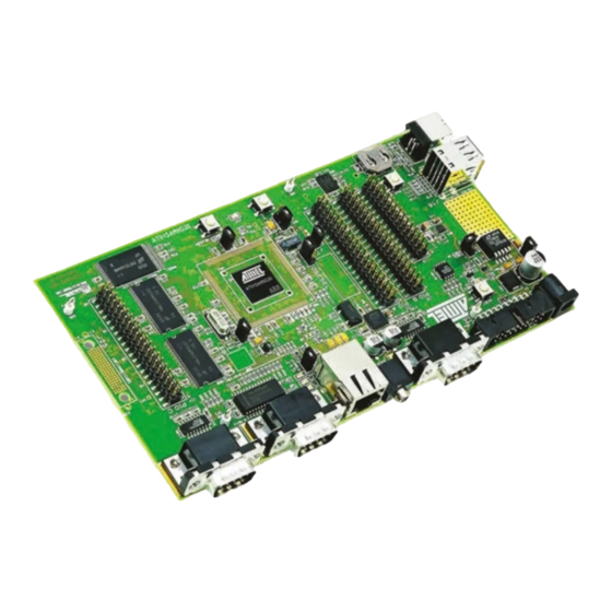
Page 8: Layout
Setting Up the AT91SAM9G20-EK Board Layout Figure 2-1. Top View AT91SAM9G20-EK Evaluation Board User Guide 6413C–ATARM–18-Feb-09... - Page 9 Setting Up the AT91SAM9G20-EK Board Figure 2-2. Bottom View AT91SAM9G20-EK Evaluation Board User Guide 6413C–ATARM–18-Feb-09...
-
Page 10: Powering Up The Board
Setting Up the AT91SAM9G20-EK Board Powering Up the Board The AT91SAM9G20-EK requires 5V DC (±5%). DC power is supplied to the board via the 2.1 mm by 5.5 mm socket J1. Coaxial plug center positive standard. Backup Power Supply The user can plug in a battery (3V Lithium Battery CR1225 or equivalent) in order to permanently power the backup part of the device. -
Page 11: At91Sam9G20-Ek Block Diagram
Setting Up the AT91SAM9G20-EK Board AT91SAM9G20-EK Block Diagram Figure 2-3. AT91SAM9G20-EK Block Diagram 10/100 Mbps FAST ETHERNET RS232 5VDC SERIAL SERIAL MCIB MCIA NANFLASH SDRAM EEPROM DATAFLASH DATAFLASH DATAFLASH AT91SAM9G20-EK Evaluation Board User Guide 6413C–ATARM–18-Feb-09... - Page 12 Setting Up the AT91SAM9G20-EK Board AT91SAM9G20-EK Evaluation Board User Guide 6413C–ATARM–18-Feb-09...
-
Page 13: Board Description
– Selectable 32,768 Hz Low-power Oscillator or Internal Low Power RC Oscillator on Battery Backup Power Supply, Providing a Permanent Slow Clock – 3 to 20 MHz On-chip Oscillator, One up to 800 MHz PLL and One up to 100 MHz PLL AT91SAM9G20-EK Evaluation Board User Guide 6413C–ATARM–18-Feb-09... - Page 14 – Master, Multi-master and Slave Mode Operation – Bit Rate: Up to 400 Kbits – General Call Supported in Slave Mode – Connection to Peripheral DMA Controller (PDC) Channel Capabilities Optimizes Data Transfers in Master Mode AT91SAM9G20-EK Evaluation Board User Guide 6413C–ATARM–18-Feb-09...
- Page 15 – 3.0V to 3.6V for VDDUSB – 3.0V to 3.6V VDDANA (Analog-to-digital Converter) – Programmable 1.65V to 1.95V or 3.0V to 3.6V for VDDIOM (Memory I/Os) • Available in a 217-ball LFBGA RoHS-compliant Package AT91SAM9G20-EK Evaluation Board User Guide 6413C–ATARM–18-Feb-09...
-
Page 16: At91Sam9G20 Block Diagram
Board Description AT91SAM9G20 Block Diagram Figure 3-1. Block Diagram AT91SAM9G20-EK Evaluation Board User Guide 6413C–ATARM–18-Feb-09... -
Page 17: Microcontroller
One additional serial interface (COM Port 1) with RTS/CTS handshake control via RS-232 DB9 male socket USB V2.0 full-speed compliant, 12 Mbits per second (UDP) Two USB Host ports V2.0 full-speed compliant, 12 Mbits per second (UHP) AT91SAM9G20-EK Evaluation Board User Guide 6413C–ATARM–18-Feb-09... -
Page 18: Audio Stereo Interface
All EBI Signals of the AT91SAM9G20 are routed to extension footprint connectors (J25) This allows the developer to check the integrity of the components and to extend the features of the board by adding external hardware components or boards. AT91SAM9G20-EK Evaluation Board User Guide 6413C–ATARM–18-Feb-09... -
Page 19: Pio Usage
ETHERNET DM9161A MII Interface (PA25..PA29) PA26 TIOA0 ERX3 High-Drive PA27 TIOA1 ERXCK High-Drive PA28 TIOA2 ECRS High-Drive PA29 SCK1 ECOL PA30 SCK2 RXD4 (BP3) User's interface Push Button PA31 SCK0 TXD4 (BP4) User's interface Push Button AT91SAM9G20-EK Evaluation Board User Guide 6413C–ATARM–18-Feb-09... - Page 20 Warning: Shared with COM PORT 0 (PB22..PB27) PB23 DCD0 ISI_D3 PB24 DTR0 ISI_D4 PB25 ISI_D5 PB26 RTS0 ISI_D6 PB27 CTS0 ISI_D7 PB28 RTS1 ISI_PCK Warning: Shared with COM PORT 1 (PB28..PB29) PB29 CTS1 ISI_VSYNC PB30 PCK0 ISI_HSYNC PB31 PCK1 ISI_MCK AT91SAM9G20-EK Evaluation Board User Guide 6413C–ATARM–18-Feb-09...
- Page 21 IRQ2 NAND Flash (NANDCS) PC15 NWAIT IRQ1 PC16 SPI0_NPCS2 EBI Data Bus (PC16..PC31) PC17 SPI0_NPCS3 PC18 SPI1_NPCS1 PC19 SPI1_NPCS2 PC20 SPI1_NPCS3 PC21 EF100 PC22 TCLK5 PC23 PC24 PC25 PC26 PC27 PC28 PC29 PC30 PC31 AT91SAM9G20-EK Evaluation Board User Guide 6413C–ATARM–18-Feb-09...
- Page 22 Board Description 3-10 AT91SAM9G20-EK Evaluation Board User Guide 6413C–ATARM–18-Feb-09...
-
Page 23: Configuration
NAND Flash chip select enable Note: 1. These jumpers are provided for power consumption measurement. By default, they are closed. To use this feature, the user has to open the strap and insert an ampere meter. AT91SAM9G20-EK Evaluation Board User Guide 6413C–ATARM–18-Feb-09... -
Page 24: Jtag/Ice
Enables the use of Ready Busy signal Opened Disables write protect SERIAL DataFlash (MN9) Soldered Enable the use of the Serial DataFlash®(MN9) Opened Disables write protect TWI SERIAL EEPROM (MN10) Soldered Enables SCL access Soldered Enables SDA access AT91SAM9G20-EK Evaluation Board User Guide 6413C–ATARM–18-Feb-09... -
Page 25: Ethernet
J35. Otherwise, signal conflicts could occur and damage both the Ethernet controller and the SD Card. Miscellaneous Refer to “Board Layout - Top View” in Section 5.1 ”Schematics” for the PIO Usage. AT91SAM9G20-EK Evaluation Board User Guide 6413C–ATARM–18-Feb-09... - Page 26 Configuration AT91SAM9G20-EK Evaluation Board User Guide 6413C–ATARM–18-Feb-09...
-
Page 27: Schematics
Section 5 Schematics Schematics This section contains the following schematics: Board Layout - Top View Power Supply and Audio AT91SAM9G20-CU Memory Ethernet Serial Interface Expansion and User Interface AT91SAM9G20-EK Evaluation Board User Guide 6413C–ATARM–18-Feb-09... - Page 28 ISI_DATA[10] ISI_DATA[10] ISI_DATA[10] PB28 PB28 PB28 RTS1/ ISI_PCK RTS1/ ISI_PCK RTS1/ ISI_PCK PC12 PC12 PC12 NCS7 NCS7 NCS7 PC28 PC28 PC28 AT91SAM9G20-EK AT91SAM9G20-EK AT91SAM9G20-EK SCALE SCALE SCALE REV. REV. REV. SHEET SHEET SHEET TXD1 TXD1 TXD1 PB13 PB13 PB13 ISI_DATA[11]...
- Page 29 DES. DES. DES. DATE DATE DATE VER. VER. VER. DATE DATE DATE 11.1 11.1 11.1 11.1 AT91SAM9G20-EK AT91SAM9G20-EK AT91SAM9G20-EK SCALE SCALE SCALE REV. REV. REV. SHEET SHEET SHEET GND_DAC GND_DAC POW ER SUPPLY & AUDIO POW ER SUPPLY & AUDIO POW ER SUPPLY &...
- Page 30 100NF 100NF 100NF MODIF. MODIF. MODIF. DES. DES. DES. DATE DATE DATE VER. VER. VER. DATE DATE DATE 4.7µF 4.7µF AT91SAM9G20-EK AT91SAM9G20-EK AT91SAM9G20-EK SCALE SCALE SCALE REV. REV. REV. SHEET SHEET SHEET 100NF 100NF 100NF 100NF 100NF 100NF 100NF 100NF 10µF...
- Page 31 DATE DATE DATE VER. VER. VER. DATE DATE DATE C148 C148 SD CARD / MMCA CARD 100NF 100NF 100NF 100NF AT91SAM9G20-EK AT91SAM9G20-EK AT91SAM9G20-EK SCALE SCALE SCALE REV. REV. REV. SHEET SHEET SHEET DATAFLASH CARD INTERFACE MEMORY MEMORY MEMORY SERIAL EEPROM (BOOTABLE) This agreement is our property.
- Page 32 MODIF. MODIF. MODIF. DES. DES. DES. DATE DATE DATE VER. VER. VER. DATE DATE DATE AT91SAM9G20-EK AT91SAM9G20-EK AT91SAM9G20-EK SCALE SCALE SCALE REV. REV. REV. SHEET SHEET SHEET ETHERNET ETHERNET ETHERNET This agreement is our property. Reproduction and publication without our written authorization shall expose offender to legal proceedings.
- Page 33 MODIF. MODIF. MODIF. DES. DES. DES. DATE DATE DATE VER. VER. VER. DATE DATE DATE AT91SAM9G20-EK AT91SAM9G20-EK AT91SAM9G20-EK SCALE SCALE SCALE REV. REV. REV. SHEET SHEET SHEET SERIAL INTERFACES SERIAL INTERFACES SERIAL INTERFACES This agreement is our property. Reproduction and publication without our written authorization shall expose offender to legal proceedings.
- Page 34 MODIF. MODIF. MODIF. DES. DES. DES. DATE DATE DATE VER. VER. VER. DATE DATE DATE AT91SAM9G20-EK AT91SAM9G20-EK AT91SAM9G20-EK SCALE SCALE SCALE REV. REV. REV. SHEET SHEET SHEET EXPANSION_UI EXPANSION_UI EXPANSION_UI This agreement is our property. Reproduction and publication without our written authorization shall expose offender to legal proceedings.
-
Page 35: Errata
This erratum is not applicable for AT91SAM9G20-EK Rev. C and later versions. Choice of an Oscillator Capacitance For many reasons at the manufacturing level, Atmel does not specify any crystal references at the board design stage. Because of that, the user can find an inconsistency in the value of the used capacitance of the 18.432 MHz crystal on each pin (C23, C24), and the nominal load capacitance of the crystal. - Page 36 Errata AT91SAM9G20-EK Evaluation Board User Guide 6413C–ATARM–18-Feb-09...
-
Page 37: Revision History
Section 6.2 ”Choice of an Oscillator Capacitance” added to errata 6392 Section 5.1 ”Schematics” New schematics pdf file (at91sam9g20-ek revc.pdf) attached to 5936 Section 1.2 ”Deliverables” on page 1-1 , last bullet added Section 3.8 ”Power Supply Circuitry” on page 3-5... - Page 38 Revision History AT91SAM9G20-EK Evaluation Board User Guide 6413C–ATARM–18-Feb-09...
- Page 39 Disclaimer: The information in this document is provided in connection with Atmel products. No license, express or implied, by estoppel or otherwise, to any intellectual property right is granted by this document or in connection with the sale of Atmel products. EXCEPT AS SET FORTH IN ATMEL’S TERMS AND CONDI- TIONS OF SALE LOCATED ON ATMEL’S WEB SITE, ATMEL ASSUMES NO LIABILITY WHATSOEVER AND DISCLAIMS ANY EXPRESS, IMPLIED OR STATUTORY...
- Page 40 Authorized Distribution Brand: Website: Welcome to visit www.ameya360.com Contact Us: Address: 401 Building No.5, JiuGe Business Center, Lane 2301, Yishan Rd Minhang District, Shanghai , China Sales: Direct +86 (21) 6401-6692 Email amall@ameya360.com 800077892 Skype ameyasales1 ameyasales2 Customer Service: Email service@ameya360.com Partnership:...