Table of Contents
Advertisement
1
This chapter gives background informa-
tion on the PCA-6143P. It then shows you
how to configure the card to match your
application and prepare it for installation
into your PC.
Sections include:
• Card specifications
• Locating components
• Safety precautions
• Configuration – Jumper settings
Experienced users can skip to the
Quick Start section on page 39.
Chapter 1 Hardware Configuration
1
Advertisement
Table of Contents

Related Manuals for Advantech PCA-6143P


Summary of Contents for Advantech PCA-6143P
- Page 1 This chapter gives background informa- tion on the PCA-6143P. It then shows you how to configure the card to match your application and prepare it for installation into your PC. Sections include: • Card specifications • Locating components • Safety precautions •...
- Page 2 The watchdog timer ensures that the CPU will be reset if it stops due to a program or EMI problem, allowing the PCA-6143P to be used in stand-alone systems or unattended environments. The PCA- 6143P’s industrial-grade construction ensures continuous, reliable...
-
Page 3: Chapter 1 Hardware Configuration
• CPU: 80486SX-25, 80486SX-33, 80486DX-33, 80486DX2-50, 80486DX2-66, or 80486DX4-100 • Bus interface: ISA (PC/AT) bus • System performance: 150 MHz with an 80486DX-33 MHz CPU (Landmark speed V1.14) • Data bus: 32-bit • DMA channels: 7 • Interrupt levels: 15 •... - Page 4 • Operating temperature: 32 to 140 F (0 to 60 • Size: 7.3" (L) x 4.8" (W) (185 mm x 122 mm) • Weight: 1.1 lbs (0.5 Kg) • EMI: Pending • MTBF: 64,500 hrs @ 25 C; 39,100 hrs @ 60 PCA-6143P User's Manual...
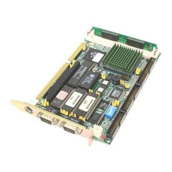
- Page 5 This section identifies the location of the card's major components. It also includes a list of the function of each of the card jumpers. The following figure gives an overall view of the card. M 1 2 1 9 - 4 0 14.318 PCA-6143P PCB Layout Chapter 1 Hardware Configuration...
- Page 6 JP12 Turbo switch JP13 Turbo LED JP14 Bypass POST JP15 Display type - color/mono JP17 Parallel port DACK selection JP18 Parallel port DRQ selection JP19,23,24 SSD device selection JP20,22,25,26, COM2 RS-232/422/485 selection 27,28,29,30 JP31 CPU voltage selection PCA-6143P User's Manual...
- Page 7 HDD connector FDD connector Parallel/printer connector CN4,CN5 PC/104 connectors COM1 RS-232 serial port COM2 RS-232/422/485 serial port On the left end of the card (away from the mounting bracket) are the two SIMM (Single In-line Memory Module) sockets which hold the card’s DRAM memory.
- Page 8 If this configuration matches your needs, you may not need to change the jumpers at all. The default configuration is as follows: • Watchdog invokes system reset • Color display is attached • Parallel port IRQ7, DRQ1, DACK1 • Bypass POST (JP14) PCA-6143P User's Manual...
- Page 9 You configure your card to match the needs of your application by setting jumpers. A jumper is the simplest kind of electric switch. It consists of two metal pins and a small metal clip (often protected by a plastic cover) that slides over the pins to connect them. To “close” a jumper you connect the pins with the clip.
- Page 10 JP11 IRQ no IRQ7 (default) IRQ5 JP17 DRQ no DRQ1 (default) DRQ3 JP18 DACK no DACK1 (default) DACK3 The following figure gives card dimensions for SBC applications: Card dimensions PCA-6143P User's Manual...
-
Page 11: Chapter 2 Installation
This chapter gives guidelines for install- ing your CPU card into an PC chassis with an AT-compatible passive backplane. For specific instructions, consult the user’s manual for your chassis. Before you begin, double check the jumper settings for the card (described in Chapter 1). - Page 12 Replace the card hold-down bracket you removed in Step 2, replace the chassis cover and power-up your system. Dimensions for SBC (Single Board Computer) installation appear in Chapter 1 (page 10). PCA-6143P User's Manual...
- Page 13 This chapter tells how to connect periph- erals, switches and indicators to the PCA- 6143P board. You can access most of the connectors from at the top of the board while it is installed in the chassis. If you have a number of cards installed, or your chassis is very tight, you may need to partially remove the card to make all the connections.
- Page 14 The following table lists the connectors on the PCA-6143P. See Chapter 1 (page 5) for help with locating the connectors. Component Label Page HDD (IDE) connector FDD connector Parallel port PC/104 connector CN4, CN5 Keyboard connectors J1, J3 Reset switch connector...
-
Page 15: Chapter 3 Connecting Peripherals
You can attach up to two floppy disk drives to the PCA-6143P's on-board controller. You can use any combination of 5.25" (360 KB and 1.2 MB) and/or 3.5" (720 KB and 1.44 MB) drives. The card comes with a 34-pin daisy-chain drive connector cable. - Page 16 You can attach two IDE (Integrated Device Electronics) hard disk drives to the PCA-6143P's internal controller. The card comes with a 40-pin flat-cable piggyback cable. This cable has three identical 40-pin flat-cable connectors. Wire number 1 on the cable is red or blue, the other wires are gray.
- Page 17 Chapter 1 (page 5). The pin assignments for the connector appear in Appendix D. The PCA-6143P board provides two keyboard connectors. A 5-pin connector (J1) supports passive backplane applications. A second 6-pin mini-DIN connector (J3) on the card mounting bracket supports single-board-computer applications.
- Page 18 JP12 is open. When jumper JP12 is closed, the CPU is fixed in Turbo mode. To switch into Turbo mode from the keyboard simultaneously press the Ctrl, Alt and keypad plus (+) keys. To switch into non-Turbo mode press the Ctrl, Alt and keypad minus (-) keys. PCA-6143P User's Manual...
- Page 19 3Speaker out 4Speaker out In single-board-computer (non-passive-backplane) applications you will need to connect power directly to the PCA-6143P board using connector J2. This connector is fully compatible with the standard PC power supply connector for a 3.5" FDD (or HDD).
- Page 20 The PCA-6143P offers two serial ports: one RS-232 and one RS-232/422/485. These ports let you connect to serial devices (a mouse, printers, etc.) or a communication network. You can select the address for each port (3F8H [COM1], 2F8H [COM2] or 3E8H) or disable it, through the BIOS Advanced Setup program, covered in Chapter 5.
- Page 21 RS-422 is commonly used for two-way communication between two devices, whereas RS-485 is used for communication between a single master and a network of slave modules. Before you use the RS-232/422/485 port, you will need to select RS-232, RS-422 (the default) or RS-485 mode. Set jumpers JP20, 22, 25, 26, 27, 28, 29 and 30 according to the following table: RS-232 RS-422...
- Page 22 Software handles the flow control; no other wires are needed. Pin assignments appear in the following table. Pins 1 and 4 share the Data+ wire. Pins 2 and 3 share the Data- wire. Data- Data+ PCA-6143P User's Manual...
- Page 23 Signal Signal – – 1 RX- – – 4 TX+ – – 2 RX+ – – 3 The following figure shows the circuits for the card's RS-422 and RS-485 driver and receiver. Driver and receiver circuit Now that you have made all the required external connections, you can close up your chassis (as described in Chapter 2).
- Page 24 PCA-6143P User's Manual...
-
Page 25: Chapter 4 Power-Up
After you have set the jumpers (Chapter 1), installed SIMMs (Appendix C), installed the card (Chapter 2) and made all external connections (Chapter 3), you are ready to power-up your system. Chapter 4 Power-up 25... - Page 26 3. Depress the optional reset switch Use of each of these methods will erase data from the system RAM memory. If you can, save any data stored in memory to a hard or floppy disk before you reset your system. PCA-6143P User's Manual...
- Page 27 This chapter describes the card’s diagnos- tic tests and how to set BIOS configura- tion data. BIOS POST (Power On Self Test) test codes appear in Appendix F. Chapter 5 BIOS diagnostics and setup...
- Page 28 These routines check the current system configuration against the values stored in the card’s CMOS memory. If they don’t match, the program outputs an error message. You will then need to run the BIOS setup program to set the configuration information in memory. PCA-6143P User's Manual...
- Page 29 3. The CMOS memory has lost power and the configuration information has been erased. The PCA-6143P’s CMOS memory has integral lithium battery backup. The battery backup should last ten years in normal service, but when it finally runs down, you will need to replace the complete unit.
- Page 30 F6: Loads all features in the Advanced CMOS Setup with the BIOS Setup defaults. F7: Loads all features in the Advanced CMOS Setup with the Power-On defaults (the values in the CMOS when the system was started). F10: Saves all changed made to Setup and exits program. PCA-6143P User's Manual...
- Page 31 Standard CMOS setup configures options that most users will need to change. Highlight Standard CMOS Setup in the main screen and press <ENTER>. A warning message appears (shown below) whenever you select either Standard CMOS Setup or Advanced CMOS Setup from the main screen.
- Page 32 Head WPcomp LZone Sect Size 10 MB 20 MB 31 MB 62 MB 47 MB 65535 20 MB 31 MB 65535 30 MB 65535 112 MB 65535 20 MB 65535 35 MB 65535 50 MB 20 MB PCA-6143P User's Manual...
- Page 33 Type Cyln Head WPcomp LZone Sect Size 65535 43 MB 20 MB 41 MB 65535 57 MB 1024 1023 60 MB 30 MB 43 MB 30 MB 10 MB 54 MB 65535 69 MB 44 MB 65535 69 MB 41 MB 65535 68 MB 53 MB...
- Page 34 Note: If you are running your system on a non-dedicated file server, and you do not want the AMI BIOS to report any keyboard, video or floppy disk drive errors during POST, set the AMI BIOS Keyboard, Primary display and floppy disk features to “Not Installed.” PCA-6143P User's Manual...
- Page 35 Advanced CMOS Setup controls system settings and the ALI M-1219 chipset’s configuration registers. Adjusting these parame- ters may improve system performance, but make a note of the original settings before you make any changes. Some combina- tions of settings may cause your system to crash or become unreliable.
- Page 36 Memory Wait State Disable (default) Enable Shadow BIOS Cacheable Disable (default) Enable 16 Bit ISA Cycle 0 w/s (default) Insert wait 1 w/s Slow refresh Disabled (default) Enabled Remapping Disabled Enabled (default) Turbo Priority Option Same (default) Hardware PCA-6143P User's Manual...
- Page 37 Feature Available options Serial Port 1 3F8H (default) 2F8H 3E8H Disabled Serial Port 2 2F8H (default) 3F8H 2E8H Disabled Parallel Port 378H (default) 278H 3BCH Disabled Enhanced Parallel Port Normal (default) ECP&ECC IDE Controller Enabled (default) Disabled Floppy Controller Enabled (default) Disabled Watchdog Timer Setting 16 min 48 seconds...
- Page 38 The BIOS will then perform a memory test, and attempt to boot your system. Be sure that your DOS system files are located on either drive A: or on your hard disk drive. If they are not, the BIOS will not be able to boot your system. PCA-6143P User's Manual...
- Page 39 Appendix A Flash/ROM disk 39...
- Page 40 The PCA-6143P features an internal Flash/ROM disk drive. This drive emulates a floppy disk drive by using solid-state memory chips (Flash or EPROM) to store programs and data instead of the magnetic particles on the mechanical drive’s disk. The Flash/ROM disk offers much faster access times than a floppy or hard disk and greatly increased reliability in harsh environments.
-
Page 41: Appendix A Flash/Rom Disk
The size of the emulated drive depends on the size and number of the chips you install. For example, if you install three 512 KB chips, you will have 3 x 512 KB = 1.536 MB, equivalent to a 1.44 MB floppy. - Page 42 Flash/RAM/ROM disk: 1st, 2nd, 3rd or 4th. Position 5 Position 6 Drive The actual drive letter assigned by DOS to the Flash/RAM/ROM disk depends on the floppy or hard disks installed in the system and the DOS version. 42 PCA-6143P User's Manual...
- Page 43 Floppy disks The Flash/ROM disk will replace the corresponding floppy disk. For example, if you have a single floppy disk (drive A:) and assign the Flash/ROM disk to be the 1st drive (both switches 5 and 6 are on), any drive operations directed at drive A: will go to the Flash/ ROM disk.
- Page 44 The next time you start the system, it will boot from the solid state disk. After you’ve set all the jumpers and switches on the PCA-6143P, insert the appropriate memory devices into the card’s sockets. Remember that you will need to program EPROMs before you insert them.
- Page 45 If you use Flash memory or SRAM, it is advisable to format the Flash/SRAM disk before copying files to it. The DOS command is as follows: FORMAT drv: /U ... where drv = solid state disk drive A, B, C etc. The utility program COOKROM.EXE, included on the card's utility disk, splits the files on a diskette into a series of binary files.
- Page 46 46 PCA-6143P User's Manual...
-
Page 47: Appendix B Programming The Watchdog Timer
The PCA-6143P is equipped with a watchdog timer that resets the CPU or generates an interrupt if processing comes to a standstill for whatever reason. This feature ensures system reliability in industrial stand-alone and unmanned environments. Appendix B Programming the watchdog timer 47... - Page 48 GOSUB 2000 REM Task #2, takes 2 sec to complete X=INP(&H043) REM Disable the watchdog 1000 REM Subroutine #2, takes 2 seconds to complete 1070 RETURN 2000 REM Subroutine #2, takes 2 seconds to complete 2090 RETURN 48 PCA-6143P User's Manual...
- Page 49 This appendix gives instructions for increasing the capabilities of your CPU card. It covers: • DRAM memory installation (SIMMs) • CPU installation and upgrading • Installing PC/104 modules Appendix C Upgrading 49...
- Page 50 Place the card and SIMMs on a static-dissipative surface or into a static-shielding bag when they are not installed. 1. Locate the CPU card’s memory banks, shown in the figure in Chapter 1 (page 5). 50 PCA-6143P User's Manual...
-
Page 51: Chapter 3, Connections
This section tells how to install or upgrade the card's CPU. You can upgrade your PCA-6143P to a higher powered 486 CPU at any time. Simply remove the old 486 CPU, install the new and set the jumpers for the CPU type and speed. - Page 52 4. Switch jumpers JP2, JP3 and JP31 to match the new CPU according to the following table: JP31 SX-25 Closed SX-33 Closed DX-25 Closed DX-33 Closed DX2-50 Closed DX2-66 Closed DX4-100 (3.45 V) Open 5. Reinstall the CPU card according to the instructions in Chapter 2. 52 PCA-6143P User's Manual...
- Page 53 The PCA-6143P's PC/104 connectors let you attach PC/104 expansion modules. These modules perform the functions of traditional plug-in expansion cards, but save space and valuable slots. Modules available from Advantech include: • PCM-3510 Super VGA module • PCM-3520 Flat-panel/CRT VGA module •...
- Page 54 PCA-6143P dimensions (mm) 54 PCA-6143P User's Manual...
- Page 55 This appendix contains information of a detailed or specialized nature. It includes: • Parallel connector pin assignments • HDD connector pin assignments • FDD connector pin assignments • Keyboard connector pin assignments • Piggyback connector pin assignments • Card connector pin assignments •...
- Page 56 DATA 5 DATA 6 DATA 7 - ACKNOWLEDGE BUSY PAPER EMPTY + SELECT - AUTO FEED - ERROR - INIT PRINTER - SELECT INPUT 18-25 GROUND Pin no. Signal Pin no. Signal - RST N.C. N.C. 56 PCA-6143P User's Manual...
- Page 57 Pin no. Signal Pin no. Signal IORDY BALE N.C. -IO CS16 N.C. A2 CS0 -ACT Pin no. Signal 1-33 (odd) GROUND HIGH DENSITY 4, 6 UNUSED INDEX MOTOR ENABLE A DRIVER SELECT B DRIVER SELECT A MOTOR ENABLE B DIRECTION STEP PULSE WRITE DATA WRITE ENABLE...
- Page 58 DACK6* SA18 IOW* SD10 DRQ6 SA17 IOR* SD11 DACK7* SA16 DACK3* SD12 DRQ7 SA15 DRQ3 SD13 SA14 DACK1* SD14 MASTER* SA13 DRQ1 SD15 SA12 REFRESH* (KEY) SA11 SYSCLK SA10 IRQ7 IRQ6 IRQ5 IRQ4 IRQ3 DACK2* BALE 58 PCA-6143P User's Manual...
-
Page 59: Appendix D Detailed System Information
I/O pin Signal name Input/output -I/O CH CK Input Input/Output Input/Output Input/Output Input/Output Input/Output Input/Output Input/Output Input/Output I/O CHRDY Input Output SA19 Input/Output SA18 Input/Output SA17 Input/Output SA16 Input/Output SA15 Input/Output SA14 Input/Output SA13 Input/Output SA12 Input/Output SA11 Input/Output SA10 Input/Output Input/Output Input/Output... - Page 60 -SMSMR Output -IOW Input/Output -IOR Input/Output -DRACK3 Output DRQ3 Input -DRACK1 Output DRQ1 Input -REFRESH Input/Output Output IRQ7 Input IRQ6 Input IRQ5 Input IRQ4 Input IRQ3 Input -DACK2 Output Output BALE Output +5Vdc Power Output Ground 60 PCA-6143P User's Manual...
- Page 61 I/O pin Signal name Input/Output SBHE Input/Output LA23 Input/Output LA22 Input/Output LA21 Input/Output LA20 Input/Output LA19 Input/Output LA18 Input/Output LA17 Input/Output -MEMR Input/Output -MEMW Input/Output SD08 Input/Output SD09 Input/Output SD10 Input/Output SD11 Input/Output SD12 Input/Output SD13 Input/Output SD14 Input/Output SD15 Input/Output I/O pin Signal name...
- Page 62 Parallel printer port 1 (LPT 2) 380-38F SDLC, bisynchronous 2 3A0-3AF Bisynchronous 1 3B0-3BF Monochrome display and printer adapter (LPT 1) 3C0-3CF Reserved 3D0-3DF Color/graphics monitor adapter 3F0-3F7 Diskette controller 3F8-3FF Serial port 1 Watchdog timer enable and trigger 62 PCA-6143P User's Manual...
- Page 63 Address Description 00-0D * Real-time clock information Second Second alarm Minutes Minute alarm Hours Hours alarm Day of week Date of month Month Year Status register A Status register B Status register C Status register D * Diagnostic status byte * Shutdown status byte Diskette drive type byte, drives A and B Reserved...
- Page 64 CH3 base and current word count Read status register/Write command register Write mode register Read temporary register/Write command register Write mode register Clear byte pointer flip-flop Read status register/Write command register Write mode register Write all mask register bus 64 PCA-6143P User's Manual...
- Page 65 Page register I/O Address DMA Channel 0 0087 DMA Channel 1 0083 DMA Channel 2 0081 DMA Channel 3 0082 DMA Channel 5 008B DMA Channel 6 0089 DMA Channel 7 008A Refresh 008F Priority Interrupt# Interrupt source Parity error detected IRQ 0 Interval timer, counter 0 output IRQ 1...
- Page 66 66 PCA-6143P User's Manual...
- Page 67 This appendix describes the general maintenance that your CPU card requires to ensure reliable operation. It then gives some solutions to common card trouble- shooting problems. Appendix E Maintenance and troubleshooting 67...
- Page 68 Inspect all cables and connectors to verify that they are securely fastened to their connecting components. Worn or stressed cables or connectors should be replaced. All peripheral equipment used with the PCA-6143P should be properly maintained. Malfunctioning equipment should be immediately replaced to prevent damage to the CPU.
-
Page 69: Appendix E Maintenance And Troubleshooting
Will not boot up Make sure that all cards on the passive backplane are firmly seated in their slots. Clean the pins on the cards and slot connectors on the passive backplane if necessary. Check the DC output of the power supply. All required voltages (+5 V , + 12 V, etc.) should be present. - Page 70 Check COM port assignment. When using standard C, Pascal or BASIC serial port commands, make sure that either the port’s DTR/DSR and RTS/CTS lines are looped back (shorted together in the connector), or the COM port 70 PCA-6143P User's Manual...
- Page 71 is set to loop back mode. Test using diagnostic software such as Checklt or QAPlus. The RS-232 interface relies on good grounding for reliable operation. Check that all equipment has a good connection to ground, and that the ground potential is the same at both locations. Parallel Port Failure Make sure the printer cable is connected correctly.
- Page 72 RTC and/or writes improper data to the RTC. Software Make sure that the memory, system configuration, display and HDD space meet the minimum requirements of the software. Make sure the software is properly installed. Check for and remove viruses. 72 PCA-6143P User's Manual...
- Page 73 This appendix lists the codes generated by the AMI BIOS if it encounters a hardware error during its POST (Power On Self Test) routines. Appendix F AMI BIOS error codes 73...
- Page 74 You can also determine the number of the test that failed by reading the LED indicators on the top of the PCA-6143P board. Please make a note of any BIOS error codes before you contact Advantech for technical support.
-
Page 75: Appendix F Ami Bios Error Codes
Beeps Meaning Processor error – The card's CPU has generated an error. 8042 Gate A20 failure – The keyboard controller (8042) contains the Gate A20 switch which allows the CPU to operate in protected mode. This error message means that the BIOS is not able to switch the CPU into protected mode. - Page 76 BIOS Setup Program to see if the correct hard You may need to run the Hard Disk Utility to correct this problem. D: drive failure The BIOS cannot get any response from hard disk drive D:. You may need to replace the disk. 76 PCA-6143P User's Manual...
- Page 77 Diskette boot failure The diskette used to boot-up in floppy drive A: is corrupt, which means you cannot use it to boot-up the system. Use another boot diskette and follow the instructions on the screen. Display switch not proper Jumper JP15 is set incorrectly. (Remember to shut down the system first).
- Page 78 XXXX is the address (in hexadecimal) at which the error occurred. Parity error ???? The BIOS has encountered a parity error with some memory in the system, but it is unable to determine the address of the error. 78 PCA-6143P User's Manual...
- Page 79 The following list of checkpoint codes gives the number for each checkpoint for the AMI BIOS POST. Codes are Copyright AMI- BIOS CHECK-POINT © 1991 American Megatrends Inc., All Rights Reserved. 1346 Oakbrook Dr. #120. GA 30093. Phone: (404)-263-8181, Fax: (404)-263-9381 Code Description of Check-point Processor register test about to start.
- Page 80 I/O port of 8042 is read. Going to initialize global data for turbo switch. Global data initialization is over. Any initialization after interrupt vector to be done next. Initialization after interrupt vector is complete. Going for monochrome mode setting. 80 PCA-6143P User's Manual...
- Page 81 Monochrome mode setting is done. Going for Color mode setting. Color mode setting is done. About to go for toggle parity before optional ROM test. Toggle parity over. About to give control for nay setup required before optional video ROM check. Processing before video ROM control is done.
- Page 82 Memory size display stared. This will be updated during memory test. Going for sequential and random memory test. Memory test below 1 M complete. Going to adjust memory size for relocation/shadow. Memory size adjusted due to relocation/shadow. Memory test above 1 M to follow. 82 PCA-6143P User's Manual...
- Page 83 Memory test above 1 M complete. Going to prepare to go back to real mode. CPU registers are saved including memory size. Going to enter in real mode. Shutdown successful, CPU in real mode. Going to restore registers saved during preparation for shutdown Registers restored.
- Page 84 Any init before C800 optional ROM control is over. Optional ROM check and control will be done next. Optional ROM control is done.About to give control to do any required processing after optional ROM returns control. 84 PCA-6143P User's Manual...
- Page 85 Any initialization required after optional ROM test over. Going to setup timer data area and printer base address. Return after setting timer and printer base address. Going to set the RS-232 base address. Returned after RS-232 base address. Going to do any initialization before coprocessor test. Required initialization before coprocessor is over.
- Page 86 86 PCA-6143P User's Manual...
Need help?
Do you have a question about the PCA-6143P and is the answer not in the manual?
Questions and answers