Table of Contents
Advertisement
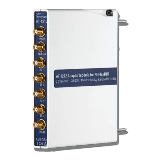
2 Channels, 1.25 GS/s, 480 MHz Analog BW , 14 Bit
High Speed Signal Generator
Adapter Module for NI FlexRIO
AT-1212 User Guide and Specifications
AT-1212
User Manual
January, 2013 Rev. 1.3
Active Technologies S.r.l
Via Bela Bartok 29/B
44124 Ferrara, ITALY
Tel +39 0532 91456, Fax: +39 0532 970134
Internet:
www.activetechnologies.it
E-mail: info@activetechnologies.it
© 2013
Active Technologies
by
. All rights reserved.
www.activetechnologies.it
Advertisement
Table of Contents

Summary of Contents for Active Technologies AT-1212
- Page 1 January, 2013 Rev. 1.3 Active Technologies S.r.l Via Bela Bartok 29/B 44124 Ferrara, ITALY Tel +39 0532 91456, Fax: +39 0532 970134 Internet: www.activetechnologies.it E-mail: info@activetechnologies.it © 2013 Active Technologies . All rights reserved. AT-1212 User Guide and Specifications www.activetechnologies.it...
-
Page 2: Table Of Contents
DACModuleControl(Host).exe ....................19 GeneratePulse(Host).vi ......................22 DDS and Trigger Route.vi ......................23 Using Your AT-1212 with a LabVIEW FPGA Example VI .............. 24 Creating a Host VI on an FPGA Target ..................27 Running the Host VI ........................31 Creating a Custom FPGA Target ....................32 Running the Host VI ........................ - Page 3 Specifications ..........................37 Configuration EEPROM Map ...................... 37 Electromagnetic Compatibility ....................37 CE Compliance ..........................38 Appendix: Installing EMI Controls ....................39 Installing PXI EMC Filler Panels ....................39 AT-1212 User Guide and Specifications - 3 - www.activetechnologies.it...
-
Page 4: At-1212 User Guide And Specifications
AT-1212 User Guide and Specifications The AT-1212 is a two-channel, 1.25 GS/s, 14-bit, 480 MHz Analog Bandwidth, High-Speed Signal Generator adapter module designed to work in conjunction with your NI FlexRIO™ FPGA module. This document contains signal information and specifications for the AT-1212R, which is composed of an NI FlexRIO FPGA module and the AT-1212. -
Page 5: Electromagnetic Compatibility Guidelines
Appendix: Installing EMI Controls section of this document. Caution To ensure the specified EMC performance, operate this product only with shielded cables and accessories. Caution This product is sensitive to electrostatic discharge (ESD). AT-1212 User Guide and Specifications - 5 - www.activetechnologies.it... -
Page 6: How To Use Your Ni Flexrio Documentation Set
Other Useful Information on ni.com ni.com/ipnet Contains LabVIEW FPGA functions and intellectual property to share. ni.com/flexrio Contains product information and data sheets for NI FlexRIO devices. * These documents are also available at ni.com/manuals. AT-1212 User Guide and Specifications - 6 - www.activetechnologies.it... -
Page 7: Front Panel And Connector Pinouts
Front Panel and Connector Pinouts Table 2 shows the front panel connectors and signal descriptions for AT-1212. Refer to the Specifications sheet for additional signal information. Caution To avoid permanent damage to the AT-1212, disconnect all signals connected to the AT-1212 before powering down the module, and connect signals only after the adapter module has been powered on by the NI FlexRIO FPGA module. - Page 8 Caution Connections that exceed any of the maximum ratings of any connector on the AT-1212R can damage the device and the chassis. Active Technologies is not liable for any damage resulting from such signal connections. For the maximum input and output ratings for each signal, refer to the Specifications sheet.
-
Page 9: At-1212 Component-Level Intellectual Property (Clip)
DRAM0 DRAM1 Figure 4. CLIP Relationship The AT-1212 ships with socketed CLIP items that are used to add module I/O to the LabVIEW project. The AT-1212ships with the following CLIP item: AT_1212_IOModule_CLIP. AT-1212 User Guide and Specifications - 9 -... -
Page 10: At-1212 Clip Design
The data read from the look up tables are serialized by the CLIP to provide the requested data rate to the DAC. Clip files: AT_1212_IOModule_CLIP.xml; AT_1212_IOModule_CLIP.vhd; Inst_PLL_156M.vhd; i2c_ctrl.vhd; OSerdes4_1.vhd; AT1212_Constraints.ucf; AT1212_IOModule.tbc AT-1212 User Guide and Specifications - 10 - www.activetechnologies.it... -
Page 11: Fpga I/O Interface
Data retrieved by I2C read startRDI2C Input Start I2C bus read startWRI2C Input Start I2C bus write reset_in Input Reset the DCMs and FAM lockedfast Output Check if the FPGA DCM has locked or not AT-1212 User Guide and Specifications - 11 - www.activetechnologies.it... -
Page 12: Clocking Scheme
DSTARA clock by using the NI timing board. If the user selects External, the DAC clock (1.25 GHz) has to be provided by outside using the SMA CLK IN bypassing the clock generator circuit. AT-1212 User Guide and Specifications - 12 - www.activetechnologies.it... -
Page 13: Cables
Use any shielded 50 Ω coaxial cable with an SMA plug end to connect to the AO 0+, AO 0-, AO 1+, AO 1-, TRIG IN, TRIG OUT and CLK IN connectors on the AT-1212 front panel. For more information about connecting I/O signals on your device, refer to the Specifications sheet. -
Page 14: Labview Interface
The user has to load each look-up tables with the same waveform and the CLIP reads them updating the Start/Stop Address and Increment parameters to convey parallel data stream at the converter at high speeds. AT-1212 User Guide and Specifications - 14 - www.activetechnologies.it... - Page 15 Timing Board (PXIe backplane). ClkEnable It enables the FPGA DCM clock output. Start Address represents the starting pointer address of StartAddress1_CH0..StartAddress8_CH0 the look-up tables. StartAddress1_CH1..StartAddress8_CH1 AT-1212 User Guide and Specifications - 15 - www.activetechnologies.it...
- Page 16 The core component of a DDS waveform generator is the accumulator. The accumulator is a running counter which stores the current phase value of the generated waveform. Increment parameter represents the value the accumulator is updated determining the frequency of the generated waveform. AT-1212 User Guide and Specifications - 16 - www.activetechnologies.it...
-
Page 17: Labview Interface Host Side
DAC B Aligned: if true the second DAC has been correctly initialized and aligned Error out IMPORTANT NOTE: the user should NOT hit the ABORT button during the initialization SetVocm.vi Set the Vocm voltage AT-1212 User Guide and Specifications - 17 - www.activetechnologies.it... - Page 18 Start the waveform generation on the selected channels. StartGeneration1212(Host).vi If Sync is true, the adapter modules waits for global software trigger (PXIe-DSTARB) to start the generation. StopGeneration1212(Host).vi Stop the waveform generation on the selected channels AT-1212 User Guide and Specifications - 18 - www.activetechnologies.it...
-
Page 19: Software Prerequisites
32-Bit Paths C:\Program Files \National Instruments\Shared\FlexRIO\IO Modules\AT 1120 C:\Program Files \National Instruments\Shared\FlexRIO\IO Modules\AT 1212 Example Code Review for AT-1212 adapter module DACModuleControl(Host).exe Software requirements: Labview 2012 + Modulation Toolkit This LabView application gives the user full access to all the main 1120/1212 features. The control panel provides a waveform generator style approach to the FAM, allowing to set the parameters of the signals that will be load and generated by the FAM. - Page 20 Press the APPLY button to display the changes on the graph . Press the LOAD WAVEFORM button to upload the data into the FPGA look-up tables. Press RUN SELECTED CH button to start the waveform generation. AT-1212 User Guide and Specifications - 20 - www.activetechnologies.it...
- Page 21 DDS frequency, Sweep Freq.Incr and Sweep Freq.Max controls. It is also possible to generate a frequency sweep, setting the increment and the stop frequency and then pressing the SWEEP ON/OFF button. AT-1212 User Guide and Specifications - 21 - www.activetechnologies.it...
-
Page 22: Generatepulse(Host).Vi
GeneratePulse(Host).vi Software requirements: LabView 2012 This VI is an user friendly example that generates pulse signals. On AT-1212 adapter modules it starts/stops both channels. Select the resource name and the adapter name (1120 or 1212). Clock Selection: select the DAC clock source. It can be Internal (from Clock Generator circuit) or External from SMA connector (1.25GHz). -
Page 23: Dds And Trigger Route.vi
Fill the Destination Trigger Array with the PXIe_DSTARB global trigger routing connections. The FlexRIO boards will receive now the same trigger signal. Press the Send Trigger button to send it to all connected FAMs. AT-1212 User Guide and Specifications - 23 - www.activetechnologies.it... -
Page 24: Using Your At-1212 With A Labview Fpga Example Vi
Complete the following steps to run an example that generates a waveform on AO 0+ of the AT-1212. 1. Connect one end of an SMA cable to AO 0+ on the front panel of the AT-1212 and the other end of the cable to your oscilloscope input (50 Ω). Tap the unused output (AO 0-) with a 50 Ω... - Page 25 If you are using an NI FlexRIO FPGA module other than the NI 7962R, select the FPGA target by using RIO Device Menu Ring. 5. On the front panel, in the resource pull-down menu, select an AT-1212 resource that corresponds with the target configured in step 4.
- Page 26 15. Press the RUN SELECTED CH. button to start the waveform generation 16. Press the STOP button to stop the generation 17. Press the EXIT VI button to stop the VI. AT-1212 User Guide and Specifications - 26 - www.activetechnologies.it...
-
Page 27: Creating A Host Vi On An Fpga Target
7. Add a Stacked Sequence Structure 8. Place the GetFPGA1212Reference.vi to get the reference to the 1212 FPGA Target (AT_HS_Signal_Generator\FPGA Bitfiles\AT1212SignalGenerator_FPGATarget.lvbitx) 9. Connect resource name RIO Device IN and error in error in control AT-1212 User Guide and Specifications - 27 - www.activetechnologies.it... - Page 28 14. Samples 128, Amplitude 4000, Cycle 1, Phase 0, add 8192 to the waveform array and connect the samples array to the Waveform Graph. If the VI execution arrives at the second frame, it means that the adapter module has been AT-1212 User Guide and Specifications - 28 - www.activetechnologies.it...
- Page 29 16. Add a For Loop structure and wire 2 to the Loop count. 17. Place the WriteTables1212(Host).vi, located on \AT_HS_Signal_Generator\1212 Module folder, into the For Loop structure. Connect the RIO Device, WavefArray and Select Channel controls like in the picture below AT-1212 User Guide and Specifications - 29 - www.activetechnologies.it...
- Page 30 Connect the FPGA VI Reference IN FPGA Reference and place Close FPGA VI Reference block located on FPGA Interface wiring it like in the picture below. The second frame contains the True constant to stop the VI. AT-1212 User Guide and Specifications - 30 - www.activetechnologies.it...
-
Page 31: Running The Host Vi
5. Click the Run button to run the VI. 6. Wait for module initialization. 7. The AT-1212 generates two 128 points sine waveforms. 8. Click the STOP button on the front panel to stop the module and the VI. AT-1212 User Guide and Specifications - 31 - www.activetechnologies.it... -
Page 32: Creating A Custom Fpga Target
7. Right-click IO Module in the Project Explorer window and select Properties. 8. Select the Active Technologies: AT-1212 from the IO Module list. The available CLIP items for the AT-1212 are displayed in the General category of the Component Level IP panel. If AT-1212 User Guide and Specifications - 32 - www.activetechnologies.it... - Page 33 General category is dimmed, select the Enable IO Module checkbox. 9. Select Active Technologies: AT-1212 to use the connector-based CLIP. 10. Click on the Clock Selections category and select DStarA Clock as clockin and 40 MHz Onboard Clock as clockin40m.
- Page 34 Memory Method node. Right-click on the Memory method, Select Memory>>Memory1. 21. Left-click on the Memory1 Memory Method and select the Read method. Insert a new shift register in the Timed Loop and wire the connectors like in the picture above. AT-1212 User Guide and Specifications - 34 - www.activetechnologies.it...
-
Page 35: Running The Host Vi
5. Click the Run button to run the VI. 6. Wait for module initialization. 7. Click the START CHANNELS button to start the waveform generation. 8. The AT-1212 generates two 2048 points sine waveforms. AT-1212 User Guide and Specifications - 35 -... -
Page 36: Filter Options
Filter Options If necessary, images and sample clock feed-through can be largely removed using a low-pass filter; Active Technologies suggests the following filters depending on the application and the user needs: Mini Circuit RLP-470+ SBPL-467 (Maximally Flat Group Delay) Mini Circuit ... -
Page 37: Specifications
Caution To avoid permanent damage to the AT-1212, disconnect all signals connected to the AT-1212 before powering down the module, and only connect signals after the module has been powered on by the NI FlexRIO FPGA module. -
Page 38: Ce Compliance
Level: 1V/m mod. 1kHz AM 80% at 3m of distance - frequency range 2.0 ÷2.7 GHz. CE Compliance This product meets the essential requirements of applicable European Directives as follows: 2006/95/EC; Low-Voltage Directive (safety) 2004/108/EC; Electromagnetic Compatibility Directive (EMC) AT-1212 User Guide and Specifications - 38 - www.activetechnologies.it... -
Page 39: Appendix: Installing Emi Controls
Figure 15. Make sure that the EMC gasket is on the right side of the PXI EMC filler panel. Captive Screw Covers Captive Mounting Screws EMC Gasket Figure 15. PXI EMC Filler Panels and Chassis AT-1212 User Guide and Specifications - 39 - www.activetechnologies.it... - Page 40 Do not over tighten screws (2.5 lb · in. maximum). For additional information about the use of PXI EMC filler panels in your PXI system, visit ni.com/info and enter emcpanel AT-1212 User Guide and Specifications - 40 - www.activetechnologies.it...
Need help?
Do you have a question about the AT-1212 and is the answer not in the manual?
Questions and answers