Table of Contents
Advertisement
12/25/2018
Nexys A7 Reference Manual
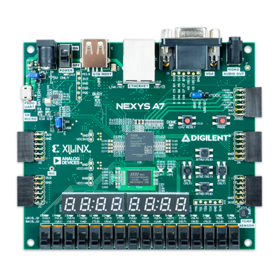
The Nexys A7 board is a complete, ready-to-use digital circuit development platform based on the latest Artix-7™ Field Programmable
Gate Array (FPGA) from Xilinx®. With its large, high-capacity FPGA, generous external memories, and collection of USB, Ethernet, and
other ports, the Nexys A7 can host designs ranging from introductory combinational circuits to powerful embedded processors. Several
built-in peripherals, including an accelerometer, temperature sensor, MEMs digital microphone, a speaker amplifier, and several I/O devices
allow the Nexys A7 to be used for a wide range of designs without needing any other components.
(https://reference.digilentinc.com/_media/reference/programmable-logic/nexys-a7/nexys-a7-obl-600.png)
https://reference.digilentinc.com/reference/programmable-logic/nexys-a7/reference-manual
Nexys A7 Reference Manual [Reference.Digilentinc]
1/30
Advertisement
Table of Contents

Summary of Contents for Nexys A7
- Page 1 Nexys A7 Reference Manual The Nexys A7 board is a complete, ready-to-use digital circuit development platform based on the latest Artix-7™ Field Programmable Gate Array (FPGA) from Xilinx®. With its large, high-capacity FPGA, generous external memories, and collection of USB, Ethernet, and other ports, the Nexys A7 can host designs ranging from introductory combinational circuits to powerful embedded processors.
- Page 2 12/25/2018 Nexys A7 Reference Manual [Reference.Digilentinc] https://reference.digilentinc.com/reference/programmable-logic/nexys-a7/reference-manual 2/30...
- Page 3 12/25/2018 Nexys A7 Reference Manual [Reference.Digilentinc] Features Artix-7 FPGA 15,850 Programmable logic slices, each with four 6-input LUTs and 8 flip-flops (*8,150 slices) https://reference.digilentinc.com/reference/programmable-logic/nexys-a7/reference-manual 3/30...
- Page 4 The Nexys A7 is compatible with Xilinx’s Vivado® Design Suite as well as the ISE® toolset, which includes ChipScope™ and EDK. Xilinx offers free WebPACK™ versions of these toolsets, so designs can be implemented at no additional cost. The Nexys A7 is not supported by the Digilent Adept Utility.
- Page 5 12/25/2018 Nexys A7 Reference Manual [Reference.Digilentinc] (https://reference.digilentinc.com/_detail/reference/programmable-logic/nexys-a7/nexys-a7-callout.png?id=reference%3Aprogrammable- logic%3Anexys-a7%3Areference-manual) Figure 1. Nexys A7 Feature Callout Callout Component Description Callout Component Description Power jack JTAG port for (optional) external cable Power switch Tri-color (RGB) LEDs USB host connector Slide switches (16) PIC24 programming port (factory use)
-
Page 6: Board Revisions
Migrating from Nexys 4 DDR The only difference between the Nexys A7 and Nexys 4 DDR is the addition of the Nexys A7-50T variant of the Nexys A7, which has a smaller gate array. The Nexys A7-100T variant is functionally identical to the Nexys 4 DDR. - Page 7 Nexys A7 Reference Manual [Reference.Digilentinc] All Nexys A7 power supplies can be turned on and off by a single logic-level power switch (SW16). A power-good LED () (LD22), driven by the “power good” output of the ADP2118 supply, indicates that the supplies are turned on and operating normally. An overview of the Nexys A7 power circuit is shown in Figure 1.1.
-
Page 8: Fpga Configuration
JTAG port. An Artix-7 100T bitstream is typically 30,606,304 bits and can take a long time to transfer. The time it takes to program the Nexys A7 can be decreased by compressing the bitstream before programming, and then allowing the FPGA to decompress the bitstream itself during configuration. - Page 9 Nexys A7 Reference Manual [Reference.Digilentinc] Since the FPGA on the Nexys A7 is volatile, it relies on the Quad-SPI flash memory to store the configuration between power cycles. This configuration mode is called Master SPI. The blank FPGA takes the role of master and reads the configuration file out of the flash device upon power-up.
-
Page 10: Quad-Spi Flash
12/25/2018 Nexys A7 Reference Manual [Reference.Digilentinc] Table 3.1.1 DDR2 settings for the Nexys A7. Setting Value Memory type DDR2 SDRAM Max. clock period 3000ps (667Mbps data rate) Recommended clock period (for easy clock generation) 3077ps (650Mbps data rate) Memory part... -
Page 11: Ethernet Phy
5 Oscillators/Clocks The Nexys A7 board includes a single 100 MHz () crystal oscillator connected to pin E3 (E3 is a MRCC input on bank 35). The input clock can drive MMCMs or PLLs to generate clocks of various frequencies and with known phase relationships that may be needed throughout a design. -
Page 12: Usb-Uart Bridge (Serial Port)
JTAG circuitry interfering with the UART data transfers, and vice-versa. The combination of these two features into a single device allows the Nexys A7 to be programmed, communicated with via UART, and powered from a computer attached with a single Micro USB cable. -
Page 13: Hid Controller
PS/2 keyboard or mouse would. This means new designs can re-use existing PS/2 IP cores. Mice and keyboards that use the PS/2 protocol use a two-wire serial bus (clock and data) to communicate with a host. On the Nexys A7, the microcontroller emulates a PS/2 device while the FPGA plays the role of the host. - Page 14 12/25/2018 Nexys A7 Reference Manual [Reference.Digilentinc] (https://reference.digilentinc.com/_detail/reference/programmable-logic/nexys-a7/n4k.png?id=reference%3Aprogrammable-logic%3Anexys- Figure 7.2.1 Keyboard Scan Codes a7%3Areference-manual) A host device can also send data to the keyboard. Table 7.2.1 shows a list of some common commands a host might send. The keyboard can send data to the host only when both the data and clock lines are high (or idle). Because the host is the bus master, the keyboard must check to see whether the host is sending data before driving the bus.
-
Page 15: Vga Port
8 VGA Port The Nexys A7 board uses 14 FPGA signals to create a VGA port with 4 bits-per-color and the two standard sync signals (HS – Horizontal Sync, and VS – Vertical Sync). The color signals use resistor-divider circuits that work in conjunction with the 75-ohm termination resistance of the VGA display to create 16 signal levels each on the red, green, and blue VGA signals. -
Page 16: Vga System Timing
12/25/2018 Nexys A7 Reference Manual [Reference.Digilentinc] (https://reference.digilentinc.com/_detail/reference/programmable-logic/nexys-a7/n4m.png?id=reference%3Aprogrammable-logic%3Anexys- Figure 8.1 Nexys A7 VGA Interface a7%3Areference-manual) 8.1 VGA System Timing VGA signal timings are specified, published, copyrighted, and sold by the VESA® organization ( www.vesa.org (http://www.vesa.org) The following VGA system timing information is provided as an example of how a VGA monitor might be driven in 640 by 480 mode. - Page 17 Video data typically comes from a video refresh memory; with one or more bytes assigned to each pixel location (the Nexys A7 uses 12 bits per pixel). The controller must index into video memory as...
- Page 18 12/25/2018 Nexys A7 Reference Manual [Reference.Digilentinc] pixel of information. The VS signal defines the “refresh” frequency of the display, or the frequency at which all information on the display is redrawn. The minimum refresh frequency is a function of the display’s phosphor and electron beam intensity, with practical refresh frequencies falling in the 50Hz to 120Hz range.
- Page 19 9 Basic I/O The Nexys A7 board includes two tri-color LEDs, sixteen slide switches, six push buttons, sixteen individual LEDs, and an eight-digit seven-segment display, as shown in Figure 9.1. The pushbuttons and slide switches are connected to the FPGA via series resistors to prevent damage from inadvertent short circuits (a short circuit could occur if an FPGA pin assigned to a pushbutton or slide switch was inadvertently defined as an output).
-
Page 20: Seven-Segment Display
9.1 Seven-Segment Display The Nexys A7 board contains two four-digit common anode seven-segment LED () displays, configured to behave like a single eight-digit display. Each of the eight digits is composed of seven segments arranged in a “figure 8” pattern, with an LED () embedded in each segment. - Page 21 To illuminate a segment, the anode should be driven high while the cathode is driven low. However, since the Nexys A7 uses transistors to drive enough current into the common anode point, the anode enables are inverted.
-
Page 22: Tri-Color Led
9.2 Tri-Color LED The Nexys A7 board contains two tri-color LEDs. Each tri-color LED () has three input signals that drive the cathodes of three smaller internal LEDs: one red, one blue, and one green. Driving the signal corresponding to one of these colors high will illuminate the internal LED (). -
Page 23: Microsd Slot
Any or all pairs in the connector can be configured either as analog input or digital input-output. The Dual Analog/Digital Pmod on the Nexys A7 differs from the rest in the routing of its traces. The eight data signals are grouped into four pairs, with the pairs routed closely coupled for better analog noise immunity. -
Page 24: Open Drain Outputs
Nexys A7 Reference Manual [Reference.Digilentinc] The Nexys A7 includes an Analog Device ADT7420 temperature sensor. The sensor provides up to 16-bit resolution with a typical accuracy better than 0.25 degrees Celsius. The interface between the temperature sensor and FPGA is shown in Figure 12.1. -
Page 25: Spi Interface
14 Microphone The Nexys A7 board includes an omnidirectional MEMS () microphone. The microphone uses an Analog Device ADMP421 chip which has a high signal to noise ratio (SNR) of 61dBA and high sensitivity of -26 dBFS. It also has a flat frequency response ranging from 100Hz to 15 kHz (). - Page 26 12/25/2018 Nexys A7 Reference Manual [Reference.Digilentinc] (https://reference.digilentinc.com/_detail/reference/programmable-logic/nexys-a7/n4aa.png?id=reference%3Aprogrammable-logic%3Anexys- Figure 14.1.1 PDM Representation of a Sine Wave a7%3Areference-manual) A PDM signal is generated from an analog signal through a process called delta-sigma modulation. A simple idealized circuit of delta-sigma modulator is shown in Figure 14.1.2.
- Page 27 12/25/2018 Nexys A7 Reference Manual [Reference.Digilentinc] (https://reference.digilentinc.com/_detail/reference/programmable-logic/nexys-a7/n4ac.png?id=reference%3Aprogrammable-logic%3Anexys- Figure 14.2.1 PDM Timing Diagram a7%3Areference-manual) The typical value of the clock frequency is 2.4 MHz (). Assuming that the application requires 7-bit precision and 24 KHz, there can be two counters that count 128 samples at 12 KHz, as shown in Figure 14.2.2.
-
Page 28: Pulse-Width Modulation
12/25/2018 Nexys A7 Reference Manual [Reference.Digilentinc] (https://reference.digilentinc.com/_detail/reference/programmable-logic/nexys-a7/n4af.png?id=reference%3Aprogrammable-logic%3Anexys- Figure 15.2 SK Butterworth Low-Pass Filter Frequency Response a7%3Areference-manual) 15.1 Pulse-Width Modulation A pulse-width modulated (PWM) signal is a chain of pulses at some fixed frequency, with each pulse potentially having a different width. -
Page 29: Built-In Self-Test
Digilent website. If the demo configuration is present in the flash and the Nexys A7 board is powered on in SPI mode, the demo project will allow basic hardware verification. Here is an overview of how this demo drives the different onboard components: The user LEDs are illuminated when the corresponding user switch is placed in the on position. - Page 30 12/25/2018 Nexys A7 Reference Manual [Reference.Digilentinc] (https://twitter.com/digilentinc) (https://www.facebook.com/Digilent) (https://www.youtube.com/user/DigilentInc) (https://instagram.com/digilentinc) (https://github.com/digilent) (https://www.reddit.com/r/digilent) (https://www.linkedin.com/company/1454013) (https://www.flickr.com/photos/127815101@N07) https://reference.digilentinc.com/reference/programmable-logic/nexys-a7/reference-manual 30/30...
Need help?
Do you have a question about the A7 and is the answer not in the manual?
Questions and answers