Table of Contents
Advertisement
Advertisement
Table of Contents

Related Manuals for Denon DN-S5000


Summary of Contents for Denon DN-S5000
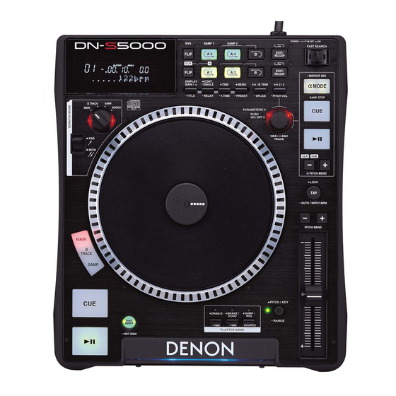
- Page 1 For U.S.A., Canada & Europe model SERVICE MANUAL DN-S5000 MODEL TABLE TOP SINGLE CD PLAYER Some illustrations using in this service manual are slightly different from the actual set . 16-11, YUSHIMA 3-CHOME, BUNKYOU-KU,TOKYO 113-0034 JAPAN Telephone: 03 (3837) 5321...
- Page 2 DN-S5000 DISASSEMBLY (Follow the procedure below in reverse order when reassembling) 1. SLIP DISC, SLIP MAT Remove a screw 69 and pull out Slip Disc and Slip Mat. Washer Slip Disc Slip Mat Slip Sheet Anti-static Sheet 2. PLATTER Remove Belt from Motor Pully.
-
Page 3: Drive Unit
DN-S5000 3. DRIVE UNIT Remove 4 screws 71 and pull out Drive Unit. Disconnect Flat cable and Connector. Detach Drive Unit. Drive Unit Connector Flat cable Drive Unit Note: ● Do not pull out aslant to prevent Flat cable damage. -
Page 4: Power Pwb
DN-S5000 5. SENSOR AND SCALE UNITS OF PLATTER Remove 2 screws 64 and pull out Sensor Cover and Sensor unit. Remove a E Ring. Pull out Scale unit. E Ring Sensor Cover Scale unit Sensor unit 6. SENSOR AND SCALE UNITS OF SLIP DISC Remove 2 screws 64 and pull out Sensor Cover and Sensor unit. -
Page 5: Drive Cover
DN-S5000 8. DSP PWB UNIT Remove 9 screws 52 and pull out DSP PWB unit DSP PWB unit 9. DRIVE COVER Remove 4 screws 12 and pull out Drive cover. Drive cover 10. DRIVE Move Drive Rack in arrow direction through the Hole on the bottom chassis. -
Page 6: Block Diagram
DN-S5000 BLOCK DIAGRAM DN-S5000 -HB,F1,F2 GND,+5,+9 LEDdriver 128Mb BU2090 SDRAM TFS0 LRCK main out BCLK AMP10 TCK0 ADSP21065L PANEL ADRE TXD0A MAIN1 DRIVE TXD0B MON1 mon out µcom 128Mb PCM1608 AMP11 ATAPI SDRAM LEDdriver INTERFACE SHOCK PROOF BU2090 MAIN DOUT... -
Page 7: Confirming The Servo
DN-S5000 CONFIRMING THE SERVO Required Measuring Implement Reference disc (TCD784 or CO-74176) 1. What is Service Program Service program is a special program intended for confirming servo functions etc. 2. Contents of Service Program Switch on the power while pushing the PITCH BEND + button and α CUE button at the same time. After actuating the servo pro- gram, select an aiming process number with the SELECT knob, A1 button, A2 button, or A3 button. -
Page 8: Test Mode
DN-S5000 Adjustment Value indication at Adjustment Item character portions. Focus Gain 35 ~ 120 Focus Balance -20 ~ +20 -20 ~ +20 Focus Offset Tracking Gain 35 ~ 120 -20 ~ +20 Tracking Balance -20 ~ +20 Tracking Offset * Reference data. - Page 9 DN-S5000 Detailed error can be displayed by PLATTER when error occurs. Error Indication FRAM CHARACTER “H * * * * E * * * ” Displays the track Displays the time at which error occurred. No. in which error Operation count Error code occurred.
-
Page 10: Top View
DN-S5000 SEMICONDUCTORS IC's MN102H730F (IC501) TOP VIEW MN102H730F Terminal Function Pin Name Symbol Function CS0_ CS0_ — — — Ext. memory chip select 0 (Flash ROM CS) CS1_ CS1_ — — — Ext. memory chip select 1 (Flash ROM for memo) —... - Page 11 DN-S5000 Pin Name Symbol Function MUTE — Mute signal (H: Mute) — — — — Oscillation input — — — — Oscillation output — — — — — Power (+3.3V) OSCI OSCI — — — — Oscillation input, 34.0MHz OSCO OSCO —...
- Page 12 DN-S5000 Pin Name Symbol Function MCNT0 — Motor control signal 0 MCNT1 — Motor control signal 1 P96,DAC2 MCNTDA — Motor rotation speed control signal A/D 0 P97,DAC3 RESERVE — — — BREQ_ BREQ_ — (Pu) Bus request signal BRACK_ BRACK_ —...
- Page 13 DN-S5000 ADSP-21065L (IC401) TOP VIEW ADSP-21065L Terminal Function Symbol Symbol Port Name Function (IC301) (IC401) — — — — — Power (+3.3V) RFS0 YLRCK YLRCK — — Receive frame sync (LRCK) signal (Serial port IN 0) — — — —...
- Page 14 DN-S5000 Symbol Symbol Port Name Function (IC301) (IC401) — — — — — SDCLK1 — — SDRAM clock enable 1 — — — — — — — — — — Power (+3.3V) SDCLK0 — — — — SDRAM clock enable 0 DMAR1_ —...
- Page 15 DN-S5000 Symbol Symbol Port Name Function (IC301) (IC401) — — — — — Power (+3.3V) DATA9 — — — — Ext. bus data 9 DATA10 — — — — Ext. bus data 10 DATA11 — — — — Ext. bus data 11 —...
- Page 16 DN-S5000 Symbol Symbol Port Name Function (IC301) (IC401) RESET_ DRES_ DRES_ — — DSP reset signal — — — — — Power (+3.3V) — — — — — ADDR23 — — — — Ext. bus address 23 ADDR22 — —...
- Page 17 DN-S5000 TMP86CM47U(IC151) TOP VIEW TMP86CM47U Terminal Function Pin Name Symbol Function — — — — — GND (0V) — — — — Oscillation input 16.0MHz XOUT XOUT — — — — Oscillation output TEST TEST — — Fixed to L —...
- Page 18 DN-S5000 SM5902AF (IC651, 652) TOP VIEW SM5902AF Terminal Function Setting Pin No. Symbol Function VDD2 — VDD power supply terminal. IP/O Microcomputer interface extended I/O 1. Not Used (OPEN) IP/O Microcomputer interface extended I/O 2. Not Used (OPEN) IP/O Microcomputer interface extended I/O 3. Not Used (OPEN) IP/O Microcomputer interface extended I/O 4.
- Page 19 DN-S5000 PCM1608Y (IC705) 36 35 34 33 32 31 30 29 28 27 26 25 SCKI AGND3 SCKO AGND4 LRCK TEST AGND6 TOP VIEW DGND AGND5 DATA1 DATA2 VCOM DATA3 ZEROA 1 2 3 4 5 6 7 8 9 10 11 12...
- Page 20 DN-S5000 Pin Name Function Voltage Output of Audio Signal Corresponding to Rch on DATA2. Up to 96kHz Voltage Output of Audio Signal Corresponding to Rch on DATA2. Up to 96kHz Voltage Output of Audio Signal Corresponding to Rch on DATA1. Up to 192kHz Voltage Output of Audio Signal Corresponding to Rch on DATA1.
- Page 21 DN-S5000 ML9207-01GP (IC101) COM22 COM21 SEG1 COM20 SEG2 COM19 SEG3 COM18 SEG4 COM17 SEG5 COM16 SEG6 COM15 SEG7 COM14 SEG8 COM13 TOP VIEW SEG9 COM12 SEG10 COM11 SEG11 COM10 SEG12 COM9 SEG13 COM8 SEG14 COM7 SEG15 COM6 SEG16 COM5 SEG17...
- Page 22 DN-S5000 TMP86CM47U (IC102) TOP VIEW TMP86CM47U Terminal Function Pin Name Symbol Function — — — — — GND(0V) — — — — Oscillation input 16.0MHz XOUT XOUT — — — — Oscillation output TEST TEST — — — — Fixed to L —...
- Page 23 DN-S5000 M5705 (IC501) AVSS-DS XRD(3) XSRFIN XRD(12) XSIPIN AVDD5-DS XRD(2) XSDSSLV XRD(13) XSRSLINT XRD(1) XRD(14) XSAWRC XRD(0) XSRFGC XRD(15) XSEFGC XHD(7) XSFOCUS XHD(8) XSTRACK XHD(6) XSSLEG XHD(9) AVDD5-DA XHD(5) XSMOTOR XHD(10) AVSS-DA XHD(4) XSRFRPLP XHD(11) XSTELP XSVREF2 XHD(3) XSRFRP XHD(12)
- Page 24 DN-S5000 Pin No. Pin Name Type Description XSSBAD Sub-beam addition signal input Phase detector reference current generator. Connect a resistor between this pin and XSPDIREF ground to set reference current Frequency detector reference current generator. Connect a resistor between this pin and...
- Page 25 DN-S5000 Pin No. Pin Name Type Description XHPDIAGJ This pin is used as the Passed Diagnostics signal, and may be an input or an open-drain output This pin is used as the Drive Active/Slave Present signal, and is an input or an open-drain XHDASPJ output.
- Page 26 DN-S5000 SP3721A (IC502) DVDRFP SDEN DVDRFN SDATA SCLK TOP VIEW MEVO MLPF SP3721A Terminal Function Pin No. Type Description Pin Name 1, 2 DVDREP , DVDREN RF Signal Inputs. Differential RF signal attenuator input pins CDRF RF Signal Inputs. Single-ended RF signal attenuator input pin...
- Page 27 DN-S5000 Pin No. Pin Name Type Description Center Error Signal Output. Center error output reference to VCI NEVO SIGO Bottom Envelope Output. Bottom envelope for mirror detection Defect Output. Pseudo CMOS output. When a defect is detected, the DFT output goes high. Also the servo AGC output can be monitored at this pin, when CAR bits 7-4 are ‘0011’...
-
Page 28: Pin Assignment
DN-S5000 128M SDRAM (IC402, 403) Pin Assignment Pin No. Pin Name Function Description 22, 23~26, A0~A11 Address Multiplexed pins for row and column address. 29~35 Row address: A0~A11. Column address: A0~A8. 20, 21 BS0, Bank Select Select bank to activate during row address latch time, or bank to read/write during address latch time. - Page 29 DN-S5000 BD6670FM (IC510) BD6670FM Terminal Function Function Name EXOR Hall input Amp 1 positive input H1+ Hall comp Hall input Amp 1 negative input Comp Hall input Amp 2 positive input Hall input Amp 2 negative input Hall Amo Hall...
-
Page 30: Function Description
DN-S5000 TA7291F(IC512) TA7291F Terminal Function PIN No. SYMBOL FUNCTION DESCRIPTION Supply voltage terminal for Logic Supply voltage terminal for Motor driver Supply voltage terminal for control GND terminal Input terminal Input terminal OUT1 Output terminal OUT2 Output terminal TRANSISTORS DTA114EK DTA114EK DTC114EK DTC114EK PNP Type NPN Type VIEW DTC114EK 10kohm 10kohm DTA114EK 10kohm 10kohm DIODES FMB-G14 FRONT VIEW AW04 RN1Z... - Page 31 DN-S5000 FL DISPLAY 24-ST-09GN (FL101) Pin Connection Pin No. Connection Pin No. Connection — — — — NOTE: 1) F- , F+ Filament 2) NP No Pin 3) DL Datum Line 4) 1G~24G Grid 5) IC Internal Connection 6) Visual Field Upper 26 , lower 26 (min.) Grid Assignment Segment Designation 10G 9G (22G~24G) (21G~11G) (10G~1G) Anode Connection 21G~1G 21G~1G — — —...
-
Page 32: Printed Wiring Boards
DN-S5000 PRINTED WIRING BOARDS GU-3482 DSP P.W.B. UNIT COMPONENT SIDE Parts List... -
Page 33: Foil Side
DN-S5000 GU-3482 DSP P.W.B. UNIT FOIL SIDE Parts List... - Page 34 DN-S5000 GU-3483 PANEL P.W.B. UNIT Parts List COMPONENT SIDE...
- Page 35 DN-S5000 GU-3483 PANEL P.W.B. UNIT Parts List FOIL SIDE...
- Page 36 DN-S5000 GU-3414 CD-ROM P.W.B. UNIT COMPONENT SIDE FOIL SIDE Parts List...
-
Page 37: Note For Parts List
DN-S5000 NOTE FOR PARTS LIST Part indicated with the mark " " are not always in stock and possibly to take a long period of time for supplying, or in some case supplying of part may be refused. When ordering of part, clearly indicate "1" and "I" (i) to avoid mis- supplying. - Page 38 DN-S5000 Note: The symbols in the column "Remarks" indicate the following destinations. PARTS LIST OF P.W.B. UNIT ASS'Y E3: U.S.A. model, Csnada model GU-3414 CD-ROM P.W.B. UNIT ASS' Y E2: Europe model Ref. No. Part No. Part Name Remarks Ref. No. Part No. Part Name Remarks R595 247 2009 983 RM73B--103JT SEMICONDUCTORS GROUP R596 247 2011 900 RM73B--333JT IC109 262 3082 908 BD4743G R597 247 2018 903 RM73B--0R0KT IC113 263 1079 903 BA033FP R601 247 2018 903 RM73B--0R0KT IC501 262 3083 004 M5705 R602 247 2003 989 RM73B--330JT ...
- Page 39 DN-S5000 Ref. No. Part No. Part Name Remarks Ref. No. Part No. Part Name Remarks C561 257 0504 940 CC73CH1H330JT C623,624 254 4300 963 CE04W0J101MT(SRE) C568 257 0512 903 CK73F1E104ZT C625 257 0501 901 CK73B1H103KT (1608) C569 257 0506 951...
- Page 40 DN-S5000 GU-3482 DSP P.W.B. UNIT ASS' Y Ref. No. Part No. Part Name Remarks Ref. No. Part No. Part Name Remarks R157 247 2009 925 RM73B--562JT SEMICONDUCTORS GROUP R158-160 247 2009 983 RM73B--103JT IC108 262 1953 903 TC7WU04F R161-176 247 2003 947...
- Page 41 DN-S5000 Ref. No. Part No. Part Name Remarks Ref. No. Part No. Part Name Remarks R604,605 247 2008 913 RM73B--202JT C156-160 257 0512 903 CK73F1E104ZT R606-610 247 2003 947 RM73B--220JT C164 257 0512 903 CK73F1E104ZT R612 247 2003 947 RM73B--220JT...
- Page 42 DN-S5000 Ref. No. Part No. Part Name Remarks C676 254 4536 928 CE04W1A101MT SMG/RE3 C677 257 0501 901 CK73B1H103KT (1608) C678 257 0512 903 CK73F1E104ZT C679 254 4254 925 CE04W1C330MT (SME) C680 257 0501 901 CK73B1H103KT (1608) C683 257 0501 901...
- Page 43 DN-S5000 GU-3483/3423A PANEL P.W.B. UNIT ASS'Y Ref. No. Part No. Part Name Remarks Ref. No. Part No. Part Name Remarks R114 247 2005 990 RM73B--241JT SEMICONDUCTORS GROUP R115 247 2005 945 RM73B--151JT IC101 262 3048 007 ML9207-01GP R116 247 2005 990...
- Page 44 DN-S5000 Ref. No. Part No. Part Name Remarks Ref. No. Part No. Part Name Remarks R411,412 247 2018 903 RM73B--0R0KT C913 254 4629 709 CE04W1C152MC(LXV)K25 R413 247 2006 902 RM73B--331JT (1608) C914 254 4632 709 CE04W1H471MC(LXV)K25 R414,415 247 2018 903...
-
Page 45: Exploded View
DN-S5000 EXPLODED VIEW Parts List ( FG5000 ) -
Page 46: Parts List Of Exploded View
DN-S5000 Note: The symbols in the column "Remarks" indicate the following destinations. E3: U.S.A. model, Csnada model PARTS LIST OF EXPLODED VIEW E2: Europe model Ref. No. Part No. Part Name Remarks Q'ty New Ref. No. Part No. Part Name Remarks Q'ty New GU-3482 DSP PWB UNIT 113 1952 107 SEARCH KNOB GU-3483 PANEL PWB UNIT for E3 412 2814 031 CARD SPACER (L=4) GU-3483A PANEL PWB UNIT for E2 445 8028 009 CORD HOLDER PANEL UNIT 475 1187 003 WASHER 13/8.2 PANEL2 UNIT 475 1161 058 WASHER 8.2/12 FLT UNIT 476 1006 006 6 E RING ZNP ... - Page 47 DN-S5000 EXPLODED VIEW OF CD DRIVE UNIT (FG-5000) Parts List Adjust the HEAT SINK to this line when placing it Bond this part (SC-608LZ) Fix this part with two-sided adhesive tape (58-3) (58-2) (58-1) Bond these part (SC-608LZ) (58-30) (58-2) Stick around the hole...
- Page 48 DN-S5000 PARTS LIST OF CD DRIVE UNIT ( FG-5000 ) Ref. No. Part No. Part Name Remarks Q'ty 9KA 2A49 6A DRIVE UNIT TD-S202H2D (FG5000MECHA)ASS'Y GU-3414 CD-ROM PWB UNIT 415 0900 001 PROTECT SHEET 412 4997 008 DRIVE BRACKET HEAT SINK...
-
Page 49: Exploded View Of Cd Mechanism
DN-S5000 EXPLODED VIEW OF CD MECHANISM Parts List 7 -3 7 -2 7 -1 7 -4 11 -14 11 -5 11 -11 11 -6 1 -4 1 -4 1 -2 1 -4 11 -3 1 -2 11 -4 1 -2 11 -12... - Page 50 DN-S5000 PARTS LIST OF CD MECHANISM UNIT ( TD-S202SA(D) ) Ref. No. Part No. Part Name Remarks Q'ty New Ref. No. Part No. Part Name Remarks Q'ty New 20 9KC 8G00 6 GEAR-LOAD-A 9KC 8A00 1 CLAMPER-PLATE ASSY 21 9KC 8G00 7 IDLE-GEAR-ROLLER CLAMPER-PLATE 22 9KC 8G00 8 CHUCK-GEAR-A LIFTER-CAM 23 9KC 8G00 9 CHUCK-GEAR-B CL-PLATE-SFT 24 9KC 8G01 0 WORM-CHUCK LIFTER-CAM-SFT 25 9KC 8G01 1 SHAFT-CAP 9KC 8A00 2 TIMING-LEVER ASSY 26 9KC 8G01 2...
- Page 51 DN-S5000 Ref. No. Part No. Part Name Remarks Q'ty New Ref. No. Part No. Part Name Remarks Q'ty New T/T MOTOR ASSY 74-1 TABLE-M32 74-2 MAGNET-M32 SCREWS 74-3 RUBBER-M32 74-4 BACK YOKE-M32 35 9KS 14N1 02 M1.4X2 PRECISION SCREW TYPE-1 74-5 T.T BUSH-SLOT-NI 36 9KS 20N3 03 M2X3 PRECISION SCREW TYPE-3 74-6 BML5E7CRS 37 9KS 17N0 15 TYPE-3 M1.7 1.5 PRECISION SCREW 75 9KC 2G08 3...
-
Page 52: Packing View
DN-S5000 PACKING VIEW Contents Note: The symbols in the column "Remarks" indicate the following destinations. E3: U.S.A. model, Csnada model PARTS LIST OF PACKING & ACCESSORIES E2: Europe model Ref. No. Part No. Part Name Remarks Q'ty New Ref. No. Part No. Part Name Remarks Q'ty New 201 505 0350 019 STYLEN PAPER 208 505 8006 006 ENVELOPE 202 503 1448 005 CUSHION 209 423 0079 108 BELT 203 505 0038 030 POLY COVER 210 529 0128 001 HEXAGON WRENCH 204 515 0945 007 WARRANTY (COM.) ... - Page 53 DN-S5000...
-
Page 54: Note For Schematic Diagram
DN-S5000 NOTE FOR SCHEMATIC DIAGRAM WARNING: Parts marked with this symbol have critical characteristics. Use ONLY replacement parts recommended by the Ω k kΩ M MΩ manufacturer. µF p CAUTION: Before returning the unit to the customer, make sure you make either (1) a leakage current check or (2) a line to chassis resistance check. -
Page 55: Schematic Diagrams
DN-S5000 SCHEMATIC DIAGRAMS (1/5) SIGNAL LINE SCHEMATIC DIAGRAMS(1/5) GU-3414 CD-ROM P.W.B UNIT... - Page 56 DN-S5000 SCHEMATIC DIAGRAMS (2/5) SIGNAL LINE SCHEMATIC DIAGRAMS(2/5) GU-3482 DSP P.W.B UNIT(1/2)
- Page 57 DN-S5000 SCHEMATIC DIAGRAMS (3/5) SIGNAL LINE SCHEMATIC DIAGRAMS(3/5) GU-3482 DSP P.W.B UNIT(2/2)
- Page 58 DN-S5000 SCHEMATIC DIAGRAMS (4/5) SCHEMATIC DIAGRAMS(4/5) GU-3483 PANEL P.W.B UNIT(1/2)
- Page 59 DN-S5000 SCHEMATIC DIAGRAMS (5/5) SCHEMATIC DIAGRAMS(5/5) GU-3483 PANEL P.W.B UNIT(2/2)
Need help?
Do you have a question about the DN-S5000 and is the answer not in the manual?
Questions and answers