Table of Contents
Advertisement
Quick Links
e
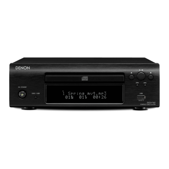
DCD-F107
• For purposes of improvement, specifications and design are subject to change without notice.
• Please use this service manual with referring to the operating instructions without fail.
• Some illustrations using in this service manual are slightly different from the actual set.
S0164-1V04DM/DG1010
SERVICE MANUAL
MODEL
COMPACT DISC PLAYER
Copyright 2010 D&M Holdings Inc. All rights reserved.
WARNING: Violators will be prosecuted to the maximum extent possible.
JP
E3
E2
P
e
D&M Holdings Inc.
Ver. 4
Please refer to the
MODIFICATION NOTICE.
EK
K2A E1C E1K EUT
Advertisement
Table of Contents

Subscribe to Our Youtube Channel
Related Manuals for Denon DCD-F107


Summary of Contents for Denon DCD-F107
- Page 1 MODIFICATION NOTICE. SERVICE MANUAL MODEL K2A E1C E1K EUT DCD-F107 COMPACT DISC PLAYER • For purposes of improvement, specifications and design are subject to change without notice. • Please use this service manual with referring to the operating instructions without fail. • Some illustrations using in this service manual are slightly different from the actual set.
-
Page 2: Laser Radiation
DCD-F107... - Page 3 DIMENSION DCD-F107...
-
Page 4: Wire Arrangement
If wire bundles are untied or moved to perform adjustment or parts replacement etc.,be sure to rearrange them neatly as they were originally bundled or placed afterward. Otherwise, incorrect arrangement can be a cause of noise generation. Wire arrangement viewed from the top Front Panel side Back Panel side DCD-F107... - Page 5 • Refer to the table below for a description of the direction in which the photos were taken. • Photographs for which no direction is indicated were taken from above the product. The viewpoint of each photograph (photography direction) [View from above] Front side Direction of photograph: A DCD-F107...
-
Page 6: Top Cover
1. DOOR Proceeding : TOP COVER DOOR → (1) Take off the Chucking plate after removing screws. Chucking plate (2) Open the CD tray by turning the Drive gear clockwise. Drive gear CD tray (3) Detach the DOOR. DOOR DCD-F107... -
Page 7: Front Panel Assy
(1) Remove the screws. View from bottom (2) Cut the clamp bands, disconnect the connector wires and FFC Cable. FFC Cable CN52 CN97 Please refer to "EXPLODED VIEW" for the disassembly method of each PCB included in FRONT PANEL ASSY. DCD-F107... -
Page 8: Cd Mechanism Assy
(1) Cut the clamp bands, disconnect the connector wires. Remove the screws. (2) Disconnect the connector wires. Connector wires Direction of photograph: A (3) Laser short-circuit in Pick-up of CD MECHANISM, then disconnect the FFC Cable. Soldering place Direction of photograph: A FFC Cable Laser short-circuit DCD-F107... -
Page 9: Disassembly Of Mechanic
(1) Detach the Sw pin on the CD tray. (2) Open the CD tray by turning the Drive gear clockwise. (3) Open the Stopper as shown in the fig., then detach CD tray. Stopper Drive gear Stopper Sw pin CD tray DCD-F107... - Page 10 ( For measuring points and waveforms, see pages 26, 27.) • The laser pick-up is OK if the amplitude level of the measured RFO waveform is between 0.4 and 1.1 Vp-p, defective oth- erwise. Protective soldering place for laser diode. DCD-F107...
- Page 11 XXX : Initial value : Stored data (EEPROM stored value) YYY : Current value Disc no read, unsteady playback, etc. Laser drive current (Iop) check Present value exceeds the initial value by 1.5 times Traverse Unit replacing Laser current (Iop) memorizing after replacement DCD-F107...
-
Page 12: Special Mode
SPECIAL MODE Function Display Key name • AC is turned on while pressing the 5 and 2 button same time on DCD-F107.(Model name display) Service mode DCD-F107 • Press the 9 button. Version No. of main μ-com Ver xxxx Display mode "****"... - Page 13 (Playback sound output) 2.5 All servo on @@ Tr XX:XX (NOTE)When the 2 button is pressed for over 1 second while the laser turns on and the laser current is measured. @@ : T.No, XX:XX : Time DCD-F107...
- Page 14 Function Display ・ 13 flashing ・ When the 2 button is pressed for over 1 second while the DCD-F107 is in the stop mode, the S/C: XXXmA/YYYmA laser turns on and the laser current is measured. LASER CURRENT ・ laser...
- Page 15 ・ When the DISC/USB and 5 button is pressed ・ 13 flashing while the DCD-F107 is in the stop mode, the accumulated laser on time is displayed. XXXXX hour ・ The laser drive times are added and the result is LASER ON TIME displayed.
- Page 16 (increased by 1) when the tray is opened. XXXX ※ If the 2 and 5 button is pressed while oper- ating, number of heat run is displayed for 3 XXXX : No. of heat run repetitions seconds. t Conduct q to e repeatedly. DCD-F107...
- Page 17 E4-05 : Error in communications with CD decoder E5-00 : Inner switch not on E6-00 : Inner switch not off E8-00 : Tray is not opened by the specified time. E8-01 : Tray is not closed by the specified time. E9-01 : Other error DCD-F107...
- Page 18 5 seconds, then error display ・ Error display reappears after 5 seconds. See 3.4. reappears. ・ AC is turned on while pressing the 5 and 2 button SYSTEM VUP same time on DCD-F107.(Entering the Service Main μ-com mode) SetDisc -> Close Version up ・...
- Page 19 Key name Function Display ・AC is turned on while pressing the 5 and 2 button BOLERO same time on DCD-F107.(Entering the Service USBμ-com SetDisc -> Close mode) Version up ・ While displaying model name, when 9 and the mode ON/STANDBY button are pressed simultaneously, the tray opens.
- Page 20 Special mode transition diagram DCD-F107...
-
Page 21: Troubleshooting
Check D924-927,Q904 and periphery circuit, and service Pin(38) of F701? it if defective. Is the voltage of approximately +7V supplied to Check the FL1/FL2 line and service it if defective. Pin(1),(43) of F701? Check the fluorescent display tube control signal of a microcomputer. (FL_RST,FL_CS,FL_CLK,FL_MDT) DCD-F107... - Page 22 Replace IC11. FLOW CHART NO.5 No operation is possible from the remote control unit. Are the System Connector (DENON BUS) Cables nomal? Check IC94 and the periphery circuit, and service it if Is +5V_SYS voltage supplied to Pin(8) of IC96? defective.
- Page 23 Check IC71 and the periphery circuit, and service it if Is +5VA voltage supplied to Pin(2) of JK91? defective. Check Pin(33) DOUT of IC17 and the periphery circuit, Check Data Signal Pin(3) D_OUT of JK91. and service it if defective. DCD-F107...
- Page 24 Check IC11,IC15 and the periphery circuit, and service it if defective. Pin(57) RST1,Pin(26) USB_RST of IC11OK? Is the "H" level CD Reset to Pin(1) of IC15? Pin(68) RST2 of IC15 OK? Check CD Controle wave and service it if defective. RFEQO,RFO,FSMONIT,FOO,TEI,TRO,FMO,DMO of IC17 DCD-F107...
-
Page 25: Measuring Point And Waveforms
CUP12202 MAIN PCB ASSY (Component side) q RFEQO w RFO o OPSW Q0 CLSW u FMO i DMO r FOO y TRO Q2 LOAD- Q1 LOAD+ CUP12202 MAIN PCB ASSY (Foil side) e FSMONIT (IC17 : 21pin) t TEI (IC17 : 24pin) DCD-F107... - Page 26 2.2 CD-R TCD-R000RM DISC DETECT 1.2 CD-R TCD-R000RM Play ②RFO 200mV ③FSMONIT ④FOO RFEQO 500Mv ⑤TEI ⑥ TRO ⑦FMO ⑧DMO 2.3 CD-RW TCD-W000RM DISC DETECTION 1.3 CD-RW TCD-W000RM Play ②RFO 200mV ③FSMONIT ④FOO RFEQO 500Mv ⑤TEI ⑥ TRO ⑦FMO ⑧DMO DCD-F107...
-
Page 27: Focus Adjustment
②RFO ③FSMONIT 200mV ④FOO ⑤TEI 500Mv ⑥ TRO ⑦FMO ⑧DMO 3.3 CD-RW TCD-W000RM TOC READ 4.3 CD-R TCD-R000RM FOCUS ADJUSTMENT ②RFO ③FSMONIT 200mV ④FOO ⑤TEI 500Mv ⑥ TRO ⑦FMO ⑧DMO 5. LOADER OPEN-CLOSE ⑨OPSW ⑩CLSW ⑪LOAD+ CLOSE OPEN ⑫LOAD- DCD-F107... - Page 28 OPEN Non (NC) (Schmitt I input) PF2/SCLK0/CTS0/CLK FL_CLK FL tube communication line (clock) (Schmitt I input) PF3/TXD1/HSSO [TXD] DENON BUS [Communication lines for (Schmitt I input) writing](F107 only) PF4/RXD1/HSSI [RXD] DENON BUS [Communication lines for (Schmitt I input) writing](F107 only)
- Page 29 When resetting it, it becomes output latch 1. PN3/SCK1 E2P_CLK Serial clock output for E2PROM (Schmitt I input)§When resetting it, it becomes output latch 1. PD0/TB0OUT0/INT4 DENON BUS (F107 only) (Schmitt I input) DVSS Power supply Power supply (GND) (GND) P74/INT0 REMOCON...
- Page 30 W.UP PG2/AN2/KI2 LD_CHCK Input for LD check Port only for input(Schmitt )/Key on W.UP PG1/AN1/KI1 KEY1 KEY input 1 Port only for input(Schmitt )/Key on W.UP 100 PG0/AN0/KI0 KEY0 KEY input 10 Port only for input(Schmitt )/Key on W.UP DCD-F107...
- Page 31 TMP92CD28AFG (IC15) DCD-F107...
- Page 32 Port only for input (with Schmidt input) PC2/INT2/TB1IN0/ SYSTEM BUSY input Port only for input (with Schmidt input) TB0IN0 PC3/INT3 STREQ input Port only for input (with Schmidt input) DVCC3B Power supply (+3.3V) Power supply (+3.3V) Non (NC) Input port Non (NC) Output port DCD-F107...
- Page 33 P70/RD Non (NC) O(L) Port only for input (Schmitt input and PU resistance) P71/SRWR Non (NC) O(L) Port only for input (Schmitt input and PU resistance) P72/SRLLB Non (PD) O(L) Port only for input (Schmitt input and PU resistance) DCD-F107...
- Page 34 Port only for input (Schmitt )/Key on W.UP PG1/KI1 Non (PD) Port only for input (Schmitt )/Key on W.UP PG0/KI0 TC94A92FG DREQ input Port only for input (Schmitt )/Key on W.UP 100 DVSS Power supply (GND) Power supply( GND) DCD-F107...
- Page 35 TC94A92FG (IC17) DCD-F107...
- Page 36 Connect to Vro by more than 0.015uF 3AI/F AGCi 3AI/F 3AI/F and PLL RVSS3 circuit FNI2 3AI/F FNI1 3AI/F FPI2 3AI/F FPI1 3AI/F 3AI/F 3AI/F Connected to PVREF, connect 3AI/F 0.1uF+100uF. AVSS3 Grounding pin for 3.3V CD analog circuits. Reference Voltage=178mVtyp. 3AI/F 3AI/F DCD-F107...
- Page 37 Refer to [1.2 Pin Assinment Table] CMOS Port Pio14/ Port 14 General Input/Output Port Schmitt input 3I/F CDMoN2 / CD Monitor 2 Refer to [1.2 Pin Assinment Table] CMOS Port CDMoN3 CD Monitor3 (Default output : SBSY) Refer to [1.2 Pin Assinment Table] 3I/F DCD-F107...
- Page 38 Refer to [1.2 Pin Assinment Table] CMOS Port Schmitt input Pio6 Port 6 General Input/Output Port 3I/F Refer to [1.2 Pin Assinment Table] CMOS Port Schmitt input Pio7 Port 7 General Input/Output Port 3I/F Refer to [1.2 Pin Assinment Table] DCD-F107...
- Page 39 Connected to VRO. Connect to PVREF GND by 0.1uF and 100uF. VCoF Connect to GND by 0.01uF 3AI/F 3A I/F : 3 V analog circuit input/output pin. 1.5 I/F : 1.5Vdigital input/output pin. 3 I/F : 3 V digital input/output pin. DCD-F107...
-
Page 40: Supply Voltage
CH BIAS INPUT CH2 INPUT IN4A CH4 INPUT 1 DO2+ CH2 OUTPUT (+) CH4 INPUT 2 DO2- CH2 OUTPUT (-) DO4+ CH4 OUTPUT (+) PGND1 POWER GROUND 1 DO4- CH4 OUTPUT (-) CH5 INPUT 2 PGND2 POWER GROUND 2 Block Diagram DCD-F107... - Page 41 Digital Bias I REF Segment Filter V COM R Vref Modulator Function Control I OUT R– Function Control Current V OUT R Segment MSEL I OUT R+ I/V and Filter ZEROL System Zero Clock ZEROR Power Supply Detect Manager DCD-F107...
-
Page 42: Terminal Name
(1) Schmitt-trigger input, 5-V tolerant (2) Schmitt-trigger input and output. 5-V tolerant input and CMOS output (3) Schmitt-trigger input and output. 5-V tolerant input. In I 2 C mode, this pin becomes an open-drain 3-state output; otherwise, this pin is a CMOS output. DCD-F107... -
Page 43: Pin Connection
2. FL DISPLAY VFD (HCA-18MS03T) (F701) PIN CONNECTION GRID ASSIGNMENT DCD-F107... - Page 44 ANODE CONNECTION DCD-F107...
- Page 45 DCD-F107...
-
Page 46: Level Diagram
LEVEL DIAGRAM DCD-F107... - Page 47 DATA (BURBROWN) BCK/LRCK/A_OUT PCM1796 OP AMP OP AMP DAC_RST MUTE NJM2068 NJM2068 AMUTE USB MCU I2CSCL (SAMSUNG) USB RST IPOD CP 2.0b I2CSDA HCA-18MS03T (TOSHIBA) MFI341S2161 TMP92CD28FG DISP DATA(I2C) DAC_CS MCK_DAC 9MHz MDT_DAC X'TAL USB JACK IPOD USB DEVICE DCD-F107...
-
Page 48: Printed Wiring Boards
PRINTED WIRING BOARDS AUDIO/POWER PCB ASSY (1/2) COMPONENT SIDE DCD-F107... - Page 49 AUDIO/POWER PCB ASSY (2/2) FOIL SIDE DCD-F107...
- Page 50 MAIN PCB ASSY FOIL SIDE COMPONENT SIDE DCD-F107...
-
Page 51: Note For Parts List
Indicates number of zeros after efective number. (0 or 1) (More than 2) 2-digit effective number. 2-digit effective number. ・ Units:pF ・ Units:pF ・ When the dielectric strength is indicated in AC,"AC" is included after the dieelectric strength value. DCD-F107... -
Page 52: Parts List Of P.w.b. Unit
C215 CHIP CERAMIC CAP (1608, 5600p) CCUS1H562KC C216 CHIP CAP CCUS1H471JA C217 CHIP CAP CCUS1H473KC C219 CHIP CAP CCUS1H473KC C220-222 CHIP CAP CCUS1H104KC C223 CHIP CAP CCUS1H103KC C224 CHIP CAP CCUS1H470JA C225 CHIP CAP CCUS1H153KC C226 CHIP CAP CCUS1H103KC DCD-F107... - Page 53 CHIP CAP CCUS1H102KC C619 CHIP CAP CCUS1H103KC C620 CHIP CAP CCUS1H104KC C621 CHIP CAP CCUS1H102KC C701 SMD ELECT CAP (MANLEX, RV, 25V/220, 8X10) CCEC1ERV221T C702 CHIP CAP CCUS1H104KC C703 CHIP CAP CCUS1H221JA C705,706 CHIP CAP CCUS1H103KC C707 CHIP CAP CCUS1H104KC DCD-F107...
- Page 54 943472007310S POWER COIL (47UH/3A) CLQ13E470MRZ L702 943472007320S POWER COIL (22UH/3A) CLQ13E220MRZ R813 FERRITE BEAD (HCB2012KF-151T20 150ohm) CLZ9R013Z X101 943141001200S SMD CRYSTAL (9MHZ, HC-49/SMD, 5PF) COX09000E150S X501 943141001200S SMD CRYSTAL (9MHZ, HC-49/SMD, 5PF) COX09000E150S X801 943141001190S SMD CRYSTAL (16.9344MHZ, HC-49/SMD, 12PF) COX16934E120S DCD-F107...
- Page 55 AUDIO/POWER PCB ASS'Y Ref. No. Part No. Part Name Remarks Q'ty New SEMICONDUCTORS GROUP IC31 00D2623362903 I.C , PCM1796DBR (DAC,FROM DENON) CVI00D2623362903_D IC41-43 00D9430007108 I.C , OP AMP HVINJM2068MDTE1 IC71 943239007350S I.C , SURGE ABSORBER(SC-59) CVINSAD500F IC72 943239007350S I.C , SURGE ABSORBER(SC-59)
- Page 56 ELECT CAP CCEA0JKS221T C728,729 CERAMIC CAP CCBS1H104ZFT C875 CHIP CAP CCUS1H104KC C876 ELECT CAP CCEA1CKS101T C877 ELECT CAP CCEA1AH470T C878,879 CHIP CAP CCUS1H470JA C882 CHIP CAP CCUS1H104KC C883 CHIP CAP CCUS1H103KC C893,894 CHIP CAP CCUS1H104KC C895 ELECT CAP CCEA1AH101T DCD-F107...
- Page 57 CHIP CAP CCUS1H104KC C969 CHIP CAP CCUS1H103KC C970,971 CHIP CAP CCUS1H104KC C972 CHIP CAP CCUS1H103KC C973 CHIP CAP CCUS1H104KC C974 CHIP CAP CCUS1H103KC C975 CHIP CAP CCUS1H104KC C976 CHIP CAP CCUS1H103KC C977 CERAMIC CAP CCBS1H103ZFT C978 ELECT CAP CCEA1JH101E DCD-F107...
- Page 58 JK92 00D9430191700 IN/OUT JACK CJJ4N034Z JK93 90M-YT004860R STEREO JACK CJJ2D008Z L701 CHIP FERRITE BEAD(60ohm, 2012) CLZ9R001Z L901 CHIP FERRITE BEAD(60ohm, 2012) CLZ9R001Z RY91 943101006870D RELAY , DC5V, 0.15W, DLS5D1-0.15W CSL1C004ZE z T901 943101007370S SUB TRANS 9V (EUR) DCD-F107E2 CLT5I014ZE DCD-F107...
-
Page 59: Wiring Diagram
USB 5V PCB POWER PCB CN92 CN81 CN71 CUP122Z-1 CN91 SUB TRANS CN71 CN53 CN94 CN93 CN53 CN21 CN97 BN81 MAIN PCB CUP12202Z CX11 CY11 MAIN TRANS CN51 CN22 CN23 CX12 CD LOADER 15p FFC DISPLAY PCB CN12 CUP12219Z-3 BN97 BN51 DCD-F107... - Page 60 EXPLODED VIEW s WARNING: Parts marked with this symbol have critical characteristics. Use ONLY replacement parts recommended by the manufacturer. DCD-F107...
-
Page 61: Parts List Of Exploded View
C3 943101006510D TRANS CLT5M039ZE C5 943302000090D MECHANISM CJDWSL11TCNA C5 943302012231S CD MECHA CJDWSL11TCNJ C9 00D9430180407 AC CORD CJA2B043ZA WASHER CNW4A028 ★ A1 WIRE ASS'Y CWB1B005300GG ★ A2 5P WIRE ASS'Y CWB1C905080EG ★ A3 11P WIRE ASS'Y CWB1C911180EG ★ A4 DCD-F107... - Page 62 ★ A6 943606007430S CARD CABLE CWC4F1A16A100A10 ★ A7 943606007440S CARD CABLE CWC4F4A21A100A08 ★ A8 943606007450S CARD CABLE CWC4F4A15A150A08 SCREWS SCREW CTBD3+8JFZR SCREW CTBD3+8JFN SCREW CTB3+6FFZR SCREW CTB3+8JFZR SCREW CTS3+8JR SCREW CTB3+10JR SCREW CTW3+8JR TRANS SCREW CTB4+6FR SCREW CTWD4+6FFZR SCREW CTWD4+6FFN SCREW CTB3+6JR DCD-F107...
-
Page 63: Exploded View Of Cd Mechanism Unit
EXPLODED VIEW OF CD MECHANISM UNIT 12-1 12-2 DCD-F107... -
Page 64: Parts List Of Cd Mechanism Unit
Outsert main chassis(S) Screw 2.6 x 16 +PTPWH 00DS262554701 Drive gear(S) 00DS262554504 Contorol cam(S) 00DS169266711 Leaf switch 5P connector Loading P.W.B 00DSX26251171 Loading motor Ass'Y 00DS262553402 Middle gear 00DS262553602 Loading pulley 00DS365338700 LM belt Screw 2.6 x 2.5 +B 00DS262723401 Insulator DCD-F107... -
Page 65: Packing View
206 943535007470D POLY BAG CPB1A184Z 207 943533007480D SNOW PAD CPS1A852 208 943533007490D SNOW PAD CPS1A853 209 943531007460D OUT CARTON BOX CPG1A898Z POS LABEL CQB1A941Z POS LABEL CQB1A941X 211 00D9430110901 CONTROL LABEL CQB1A627 211 00D9430110901 CONTROL LABEL CQB1A627 COLOR LABEL CQB1A882Z DCD-F107... -
Page 66: Note For Schematic Diagram
NOTICE: ALL RESISTANCE VALUES IN OHM. k=1,000 OHM M=1,000,000 OHM ALL CAPACITANCE VALUES IN MICRO FARAD. P=MICRO-MICRO FARAD EACH VOLTAGE AND CURRENT ARE MEASURED AT NO SIGNAL INPUT CONDITION. CIRCUIT AND PARTS ARE SUBJECT TO CHANGE WITHOUT PRIOR NOTICE. DCD-F107... -
Page 67: Main Unit
C226 0.01uF IC19 R222 +3.3V_D. C203 C201 +3.3V_D. 2200P R221 HOST MCU DCD710AE : R101 0 ohm 0.1uF +1.5V_D2 C281 DCD-F107 : R102 0 ohm C202 R201 TMP92FD23AFG 0.1uF CX12 Pio7 R220 R284 C110 100/6.3V VCOI N.C(0) P.KEY/REM2 R101 Pio6... - Page 68 SUB POWER UNIT DC/DC REGUALTOR DCD-F107 Only +5VDD 5V_REG_SW R751 IC71 V_OUT +15V L701 V_IN +5VDD 47UH/3A PW_GND L702 +15V 22UH/3A C706 0.01uF PW_GND FG98 FG99 PCB VESRION PW_GND R998 DCD-F107E2 R999 DCD-F107SP SCHEMATIC DIAGRAMS (2/5) SUB POWER UNIT DCD-F107...
- Page 69 USB SIGNAL LINE SCHEMATIC DIAGRAMS (3/5) POWER UNIT DCD-F107...
- Page 70 USB SIGNAL LINE SCHEMATIC DIAGRAMS (4/5) DISPLAY UNIT DCD-F107...
- Page 71 CD SIGNAL LINE SCHEMATIC DIAGRAMS (5/5) AUDIO UNIT DCD-F107...
Need help?
Do you have a question about the DCD-F107 and is the answer not in the manual?
Questions and answers