Table of Contents
Advertisement
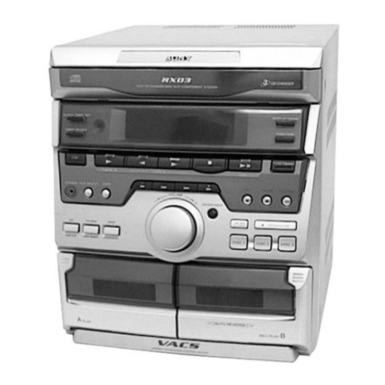
SERVICE MANUAL
HCD-RXD3 is the tuner, deck, CD and
amplifier section in MHC-RXD3.
AUDIO POWER SPECIFICATIONS:
(U.S.A. model only)
POWER OUTPUT AND TOTAL
HARMONIC DISTORTION:
with 6 Ω loads both channels driven, from 70 –
20,000 Hz; rated 50 W per channel minimum RMS
power, with no more than 0.9% total harmonic
distortion from 250 mW to rated output.
Amplifier section
Continuous RMS power output
60W + 60W
(6 Ω at 1 kHz, 10%
THD)
Inputs
MD IN (phono jack):
voltage 450mV,
impedance 47 kΩ
Outputs
MD OUT (phono jacks):
voltage 250mV
impedance 1k Ω
PHONES (stereo phone jack):
accepts headphones of
8 Ω or more.
SPEAKER:
accepts impedance of
6 to 16 Ω
MICROFILM
HCD-RXD3
Model Name Using Similar Mechanism
CD Mechanism Type
CD
Base Unit Type
SECTION
Optical Pick-up Type
TAPE
Model Name Using Similar Mechanism
DECK
Tape Transport Mechanism Type
SECTION
SPECIFICATIONS
CD player section
System
Compact disc and digital
audio system
Laser
Semiconductor laser
(λ = 780 nm)
Emission duration:
continuous
Laser output
Max. 44.6µW*
*This output is the value
measured at a distance of
200 mm from the
objective lens surface on
the Optical Pock-up
Block with 7 mm
aperture.
Frequency response
20Hz – 20kHz (±0.5 dB)
Wavelength
780 – 790 nm
DIGITAL OUT (OPTICAL)
(Square optical connector jack, rear panel)
Wavelength
600 nm
Output Level
–18 dBm
Tape deck section
Recording system
4-track 2-channel stereo
Frequency response
40 – 13,000 Hz (±3 dB),
using Sony TYPE I
cassette
MINI Hi-Fi COMPONENT SYSTEM
US Model
Canadian Model
HCD-RX55
CX3
KSM-213ECM
KSS-213ECM/C2NP
NEW
CWL-44-FR
Tuner section
FM stereo, FM/AM superheterodyne tuner
FM tunr section
Tuning range
87.5 – 108.0 MHz
Antenna
FM lead antenna
75 Ω unbalanced
Antenna terminals
Intermediate frequency
10.7 MHz
AM tuner section
Tuning renge
531 – 1,602 kHz
(with AM tuning interval
set at 9 kHz)
530 – 1,710 kHz
(with AM tuning interval
set at 10 kHz)
Antenna
AM loop antenna
Antenna terminals
External antenna
terminal
Intermediate frequency
450 kHz
— Continued on next page —
Advertisement
Table of Contents

Related Manuals for Sony HCD-RXD3


Summary of Contents for Sony HCD-RXD3
- Page 1 HCD-RXD3 SERVICE MANUAL US Model Canadian Model HCD-RXD3 is the tuner, deck, CD and amplifier section in MHC-RXD3. Model Name Using Similar Mechanism HCD-RX55 CD Mechanism Type Base Unit Type KSM-213ECM SECTION Optical Pick-up Type KSS-213ECM/C2NP TAPE Model Name Using Similar Mechanism...
-
Page 2: Leakage Test
LES COMPOSANTS IDENTIFÉS PAR UNE MARQUE ! SUR LES DIAGRAMMES SCHÉMATIQUES ET LA LISTE DES PIÈCES SONT CRITIQUES POUR LA SÉCURITÉ DE FONCTIONNEMENT. NE REMPLACER CES COMPOSANTS QUE PAR DES PIÈSES SONY DONT LES NUMÉROS SONT DONNÉS DANS CE MANUEL OU DANS LES SUPPÉMENTS PUBLIÉS PAR SONY. -
Page 3: Table Of Contents
TABLE OF CONTENTS 1. GENERAL ·········································································· 4 2. DISASSEMBLY 2-1. CD Door ············································································· 5 2-2. Front Panel ········································································· 6 2-3. Main Board ········································································· 6 2-4. Amplifier Board ································································· 7 2-5. CD Tray ·············································································· 7 2-6. Decord Board ····································································· 8 2-7. Base Unit ············································································ 9 2-8. -
Page 4: General
SECTION 1 GENERAL !º !¡ #£ !™ #™ !£ #¡ !¢ !∞ #º !§ !¶ @ª !• @• !ª @¶ @º @§ @¡ @∞ @¢ @£ @™ !¶ 1/u (Power) button 6 OPEN/CLOSE button !• TIMER SELECT button DISC SKIP/EX-CHANGE button !ª... -
Page 5: Disassembly
SECTION 2 DISASSEMBLY Note : Follow the disassembly procedure in the numerical order given. 2-1. CD DOOR 5 Top cover 2 Three screws 3 Five screws 4 Remove the claws 8 CD door 1 Three srews 7 Remove the claws 4 Remove the claws 6 Pull out the CD tray and remove the... -
Page 6: Front Panel
2-2. FRONT PANEL MAIN board 9 Board to board connectors (CN602) (CN601) 2 Screw 3 Harness (CN303) !º Front panel 4 Flat type wire (CN705) 5 Flat type wire (CN501) 6 Connector (to deckB) 8 Remove the claws 1 Three screws 7 Connector (CN201) 2-3. -
Page 7: Amplifier Board
2-4. AMPLIFIER BOARD 9 Three screws 6 Rear cover 8 Three screws 2 Two screws !º AMPLIFIER board 1 Connector (CN703) 3 Three screws 5 Remove the claws 4 Two screws 7 Three screws 2-5. CD TRAY 1 Screw 2 Bracket 5 Flat type wire (CN06) 3 Screw... -
Page 8: Decord Board
2-6. DECORD BOARD 4 Three screws 3 Flat cable (CN701) 6 CD decode board 1 Flat cable (CN706) 2 Connector (CN707) 5 Connector (CN702) — 8 —... -
Page 9: Base Unit
2-7. BASE UNIT 4 Screw 2 Screw 3 UD-gear 5 UD-Cam 7 Spring 6 Spring 8 Spring 1 Two screws 9 Base unit 2-8. CASSETTE LID Cassette door (Note: Four claws are used.) — 9 —... -
Page 10: Test Mode
SECTION 3 TEST MODE Function Key combination Description CD service mode STOP + OPEN/CLOSE The message “CD S - -” is displayed on the screen. The sled is moved to the outer circumference Initialization while the FF button is pressed. Also, the SLED is moved to the STOP + POWER OFF All preset data is re-set to the initial inner (default) value. -
Page 11: Mechanical Adjustments
SECTION 4 SECTION 5 MECHANICAL ADJUSTMENTS ELECTRICAL ADJUSTMENTS Precaution DECK SECTION 0 dB=0.775V 1. Clean the following parts with a denatured alcohol-moistened Demagnetize the record/playback head with a head swab: demagnetizer. record/playback head pinch rollers Do not use a magnetized screwdriver for the adjustments. erase head rubber belts After the adjustments, apply suitable locking compound to the... - Page 12 Mode: Playback Tape Speed Adjustment (Deck A) test tape Procedure: SPEAKER P-4-A100 Mode: Playback terminal (JK401) (10kHz, –10dB) (L-CH) oscilloscope test tape WS-48B frequency counter (3kHz, 0dB) – SPEAKER SPEAKER terminal (JK401) terminal (JK401) (R-CH) Waveform of oscilloscope Adjust the SFR501 so that the frequency counter reads 3,000 Hz ±...
- Page 13 TUNER SECTION 0 dB=1µV AM Tuning Voltage Adjustment DC voltmeter Main board – Procedure: Set the reception frequency of the unit to 530 kHz. Adjust L105 for 1.2 ± 0.05 V reading on the DC voltmeter. Set the reception frequency of the unit to 1,710 kHz. Confirm that the voltage reading on the DC voltmeter is within 8.0 ±...
- Page 14 FM Tuned Level Adjustment FM RF SSG 75 Ω coaxial Carrier frequency : 98 MHz Modulation : AUDIO 1 kHz, 75 kHz FM ANTENNA terminal deviation (100%) (JK101) Output level : 28 dB (at 75 W open) Procedure: Supply a 28 dB 98 MHz signal from the ANTENNA terminal. Tune the set to 98 MHz.
- Page 15 CD SECTION Note: CD Block is basically constructed to operate without adjustment. Therefore, check each item in order given. Use YEDS-18 disc (3-702-101-01) unless otherwise indicated. Use an oscilloscope with more than 10MΩ impedance. Clean the object lens by an applicator with neutral detergent when the signal level is low than specified value with the following checks.
-
Page 16: Diagrams
SECTION 6 DIAGRAMS 6-1. CIRCUIT BOARDS LOCATION SW (B) board SW (D) board MOTOR (6P) (S) board SW (C) board MOTOR board MAIN board PHOTO SOCKET board SW (A) board CD DECORD board SENSOR board TR board H/P board FUSE board VR board AMPLIFIER board FRONT board... -
Page 17: Block Diagrams
HCD-RXD3 6-2. BLOCK DIAGRAMS MAIN SECTION CD L JK301 SECTION JK301 (Page 20) LINE AMP LINE OUT IC301 Q551 Q320 R CH POWER AMP CD (L) MUTE REC/PB IC401 EQ AMP R CH IC201 RL401 MD (L) VOL OUT JK401... -
Page 18: Tuner/Cd Section
HCD-RXD3 TUNER/CD SECTION FM/AM MPX FM FRONT END IC102 FE101 Q101 CF101 CF102 TU L 10.7MHz RF IF 10.7MHz FM IF AM/FM MUTE DECODER 75Ω IF BUFF R CH JK101 ANTENNA Q117 CF104 FM DET MUTE 10.7MHz FM OUT • RCH is omitted •... - Page 19 HCD-RXD3 • WAVEFORM THIS NOTE IS COMMON FOR PRINTED WIRING BOARDS AND SCHEMATIC DIAGRAMS. (In addition to this necessary note is printed in each — BD SECTION — — PANEL SECTION — block.) IC701 #£ (PLAY MODE) IC601 $º (X' TAL) IC702 $ª...
-
Page 20: Printed Wiring Board Main Section
HCD-RXD3 • Refer to page 16 for Circit Boards Location. • Refer to page 21 for Note on Printed Wiring Board. 6-3. PRINTED WIRING BOARD MAIN SECTION • Semiconductor Location FRONT BOARD Ref. No. Location DECK B MAIN BOARD CN602... -
Page 21: Schematic Diagram Main (1/3) Section
HCD-RXD3 6-4. SCHEMATIC DIAGRAM MAIN (1/3) SECTION • Refer to page 22 for Waveforms. • Refer to page 47 for IC Block Diagrams. • Refer to page 21 for Note on Schematic Diagram. — 25 — — 26 —... -
Page 22: Schematic Diagram Main (2/3) Section
HCD-RXD3 6-5. SCHEMATIC DIAGRAM MAIN (2/3) SECTION • Refer to page 22 for Waveforms. • Refer to page 47 for IC Block Diagrams. • Refer to page 21 for Note on Schematic Diagram. — 27 — — 28 —... -
Page 23: Schematic Diagram Main (3/3) Section
HCD-RXD3 6-6. SCHEMATIC DIAGRAM MAIN (3/3) SECTION • Refer to page 47 for IC Block Diagrams. • Refer to page 21 for Note on Schematic Diagram. — 29 — — 30 —... -
Page 24: Printed Wiring Board Front Panel Section
HCD-RXD3 • Refer to page 16 for Circuit Boards Location. • Refer to page 21 for Note on Printed Wiring Board. 6-7. PRINTED WIRING BOARD FRONT PANEL SECTION SENSOR BOARD C600 RM601 FRONT BOARD RA603 RA602 RA601 RA604 CN604 FLD601... -
Page 25: Schematic Diagram Front Panel Section
HCD-RXD3 • Refer to page 22 for Waveforms. • Refer to page 43 for IC Pin Function. • Refer to page 21 for Note on Schematic Diagram. 6-8. SCHEMATIC DIAGRAM FR ONT PANEL SECTION — 33 — — 34 —... -
Page 26: Printed Wiring Board Amplifier Section
HCD-RXD3 • Refer to page 16 for Circuit Boards Location. • Refer to page 21 for Note on Printed Wiring Board. 6-9. PRINTED WIRING BOARD AMPLIFIER SECTION JK401 TR BOARD SPEAKER Q701 (11) 1-674-554- T001 (4146270130) POWER TRANSFORMER JK401 C424 C426... -
Page 27: Schematic Diagram Amplifier Section
HCD-RXD3 • Refer to page 21 for Note on Schematic Diagram. 6-10. SCHEMATIC DIAGRAM AMPLIFIER SECTION AC IN The components identified by Les composants identifiés par mark ! or dotted line with mark une marque ! sont critiques ! are critical for safety. -
Page 28: Printed Wiring Board Cd Section
HCD-RXD3 • Refer to page 16 for Circuit Boards Location. • Refer to page 21 for Note on Printed Wiring Board. 6-11. PRINTED WIRING BOARD CD SECTION • Semiconductor Location SW (D) BOARD SW (C) BOARD Ref. No. Location CN16... -
Page 29: Schematic Diagram Cd Section
HCD-RXD3 • Refer to page 22 for Waveforms. • Refer to page 45,46 for IC Block Diagrams. • Refer to page 21 for Note on Schematic Diagram. 6-12. SCHEMATIC DIAGRAM CD SECTION The components identified by Les composants identifiés par... -
Page 30: Ic Pin Function
HCD-RXD3 6-13. IC PIN FUNCTION IC601 CXP82040-108Q(SYSTEM CONTR OL) FRONT BOARD Pin No. Pin Name Description Pin No. Pin Name Description 2G,1G FLD grid output. TRAY C. SW Tray close switch signal input. — Not used. VR UP Volume up signal input. -
Page 31: Ic Block Diagrams
6-14. IC BLOCK DIAGRAMS — CD DECORD SECTION — IC701 CXA1992BR 33 32 31 30 PD 2 PD 1 I-V AMP I-V AMP RF SUMMING FOCUS OK COMPARATOR LASER POWER CONTROL IFB1 – IFB6 PEAK/BOTTOM MIRR HOLD COMPARATOR ↓ DEFECT PEAK/BOTTOM BIAS HOLD... - Page 32 IC702 CXD2589Q 25 26 47 49 54 56 50 39 41 55 40 42 44 62 TES1 TEST XRST Clock Error Generator RMUT Corrector LMUT Serial In demoduretor Interface Interface ASYI XTAI Asymmetry Timing ASYO Corrector XTAO Logic BIAS Over Sampling Digital Filter XPCK FILO...
- Page 33 — MAIN BOARD — IC103 LC72131 PHASE DETECTOR CHARGE PUMP POWER REFERENCE UNLOCK DIVIDER DETECTOR RESET SWALLOW COUNTER 1/16, 1/17 4BITS 12BITS PROGRAMMABLE DRIVER UNIVERSAL DATA SHIFT REGISTER LATCH INTERFACE COUNTER 2 3 4 5 6 7 8 9 IC201 TA8189N METAL TAPE A...
- Page 34 IC252 74HC165 PARALLEL INPUTS CLOCK SERIAL OUTPUT INHIBIT INPUT CLOCK SERIAL INHIBIT SHIFT/ LOAD SHIFT/ CLOCK OUTPUT LOAD PARALLEL INPUTS IC301 M62439SP REC OUT2 INA2 INB2 INC2 IND2 TONEH2 TONEL2 OUT2 CONT CONTROL LOGIC REC OUT1 INA1 INB1 INC1 IND1 TONEH1 TONEL1 OUT1...
-
Page 35: Exploded Views
SECTION 7 EXPLODED VIEWS NOTE: • -XX, -X mean standardized parts, so they may • The mechanical parts with no reference number The components identified by mark ! or have some differences from the original one. in the exploded views are not supplied. dotted line with mark ! are critical for safety. -
Page 36: Front Panel Section
7-2. FRONT PANEL SECTION not supplied not supplied not supplied not supplied Ref. No. Part No. Description Remarks Ref. No. Part No. Description Remarks A-4411-712-A PANEL ASSY, FRONT 4-220-805-01 BUTTON, FUNCTION 4-220-592-01 WINDOW (L), CASSETTE 4-220-617-01 LENS (A), BUTTON 4-220-595-01 DOOR (L), CASSETTE 4-220-618-01 LENS (B/L), BUTTON 4-220-626-01 HOLDER (L), CASSETTE 4-220-619-01 LENS (B/R), BUTTON... -
Page 37: Cd Mechanism Deck Section-1
7-3. CD MECHANISM DECK SECTION-1 M103 Ref. No. Part No. Description Remarks Ref. No. Part No. Description Remarks 1-674-792-11 MOTOR BOARD 4-992-183-01 SCREW, RELAY GEAR (B) 4-221-891-01 BASE CHANGER 4-992-174-01 GEAR, CHANGE 4-221-895-01 SHEET, BLIND 4-992-184-01 WASHER, CHANGE GEAR 4-221-896-01 LEVER, SENSOR (SW) 4-992-176-01 SPRING, CHANGE GEAR 4-992-182-01 SPRING, SENSOR (SW) LEVER 4-992-185-01 WASHER, CHANGE PLATE... -
Page 38: Cd Mechanism Deck Section-2
7-4. CD MECHANISM DECK SECTION-2 not supplied not supplied M104 Base unit block Ref. No. Part No. Description Remarks Ref. No. Part No. Description Remarks 1-769-856-11 WIRE (FLAT TYPE) (5 CORE) 1-674-791-11 SW (D) BOARD 4-221-897-01 UD-CAM 1-674-790-11 SW (C) BOARD 4-992-191-01 UD-GEAR 4-992-194-01 CLAMP 4-992-195-01 MAGNET... -
Page 39: Base Unit Section (Ksm-213Ecm)
7-5. BASE UNIT SECTION (KSM-213ECM) not supplied M101 M102 Ref. No. Part No. Description Remarks Ref. No. Part No. Description Remarks 4-992-164-01 BASE, KSM MECHANICAL 2-627-003-02 GEAR (B) 4-992-165-01 DAMPER (GREEN) 1-639-678-12 MOTOR (6P)(S) BOARD 4-992-166-01 DAMPER (RED) 1-783-740-11 WIRE (FLAT TYPE) 4-992-167-01 SPRING, MECHANICAL BASE ! 211 8-820-054-03 OPTICAL PICK-UP KSS-213ECM/C2NP... -
Page 40: Electrical Parts List
SECTION 8 AMPLIFIER ELECTRICAL PARTS LIST NOTE: • Due to standardization, replacements in the • CAPACITORS: • SEMICONDUCTORS parts list may be different from the parts uF: µF In each case, u: µ, for example: specified in the diagrams or the components •... - Page 41 AMPLIFIER CD DECORD Ref. No. Part No. Description Remarks Ref. No. Part No. Description Remarks D711 8-719-012-33 DIODE UZ-27BSA-TA R426 1-247-871-11 CARBON 1/4W D712 8-719-010-57 DIODE UZ-8.2BSA R427 1-249-417-11 CARBON 1/4W F D713 8-719-991-33 DIODE 1SS133T-77 R428 1-249-438-11 CARBON 1/4W D714 8-719-010-73 DIODE UZ-12BSA R429...
- Page 42 CD DECORD Ref. No. Part No. Description Remarks Ref. No. Part No. Description Remarks C723 1-137-399-11 FILM 0.1uF 100V C787 1-162-294-31 CERAMIC 0.001uF C724 1-107-713-11 ELECT 4.7uF C788 1-162-294-31 CERAMIC 0.001uF C725 1-137-352-11 FILM 0.033uF 100V C789 1-161-494-00 CERAMIC 0.022uF C726 1-137-462-11 FILM 0.018uF...
- Page 43 CD DECORD FRONT Ref. No. Part No. Description Remarks Ref. No. Part No. Description Remarks R715 1-249-439-11 CARBON 1/4W R778R 1-247-847-11 CARBON 4.7K 1/4W R716 1-249-439-11 CARBON 1/4W R779 1-247-839-11 CARBON 2.2K 1/4W R717 1-249-439-11 CARBON 1/4W R780 1-247-839-11 CARBON 2.2K 1/4W R718...
- Page 44 FRONT Ref. No. Part No. Description Remarks Ref. No. Part No. Description Remarks C645 1-126-957-11 ELECT 0.22uF < TRANSISTOR > C646 1-162-306-11 CERAMIC 0.01uF C647 1-126-957-11 ELECT 0.22uF Q601 8-729-194-57 TRANSISTOR 2SC945-P C648 1-126-957-11 ELECT 0.22uF Q602 8-729-194-57 TRANSISTOR 2SC945-P C649 1-162-302-11 CERAMIC 0.0022uF 30%...
- Page 45 FRONT FUSE MAIN Ref. No. Part No. Description Remarks Ref. No. Part No. Description Remarks R656 1-247-843-11 CARBON 3.3K 1/4W S621 1-572-647-11 SWITCH, KEY BOARD R657 1-247-847-11 CARBON 4.7K 1/4W (PLAY MODE,TUNER MEMORY) R658 1-249-428-11 CARBON 8.2K 1/4W F S622 1-572-647-11 SWITCH, KEY BOARD (REPEAT,STEREO/MONO) R659 1-249-951-11 CARBON...
- Page 46 MAIN Ref. No. Part No. Description Remarks Ref. No. Part No. Description Remarks C135 1-162-293-31 CERAMIC 820PF C224 1-162-290-31 CERAMIC 470PF C137 1-126-959-11 ELECT 0.47uF C225 1-164-736-31 CERAMIC 0.0012uF 10% C138 1-164-159-11 CERAMIC 0.1uF C226 1-164-736-31 CERAMIC 0.0012uF 10% C139 1-161-494-00 CERAMIC 0.022uF C227...
- Page 47 MAIN Ref. No. Part No. Description Remarks Ref. No. Part No. Description Remarks C363 1-164-159-11 CERAMIC 0.1uF < JACK > C378 1-126-961-11 ELECT 2.2uF C379 1-126-961-11 ELECT 2.2uF JK101 1-694-092-21 TERMINAL BOARD (SPEAKER) C500 1-126-960-11 ELECT JK301 1-770-613-11 JACK, PIN 4P (MD IN/OUT) C500A 1-161-494-00 CERAMIC 0.022uF...
- Page 48 MAIN Ref. No. Part No. Description Remarks Ref. No. Part No. Description Remarks R117 1-247-855-11 CARBON 1/4W R226 1-247-863-11 CARBON 1/4W R118 1-247-807-11 CARBON 1/4W R227 1-247-881-00 CARBON 120K 1/4W R119 1-249-410-11 CARBON 1/4W F R228 1-247-881-00 CARBON 120K 1/4W R120 1-247-843-11 CARBON 3.3K...
- Page 49 MAIN MOTOR MOTOR (6P) (S) Ref. No. Part No. Description Remarks Ref. No. Part No. Description Remarks R334 1-247-849-11 CARBON 5.6K 1/4W R527 1-249-413-11 CARBON 1/4W F R335 1-247-849-11 CARBON 5.6K 1/4W R528 1-247-847-11 CARBON 4.7K 1/4W R336 1-247-827-11 CARBON 1/4W R551 1-247-855-11 CARBON...
- Page 50 HCD-RXD3 SENSOR SW (A) SW (B) SW (C) SW (D) PHOTO SOCKET Ref. No. Part No. Description Remarks Ref. No. Part No. Description Remarks 1-674-794-11 PHOTO SOCKET BOARD MISCELLANEOUS ******************** ************* < CAPACITOR > 1-783-531-51 CORD, POWER 3-703-244-21 BUSHING, CORD...