
Summary of Contents for Zynq ZedBoard
- Page 1 ZedBoard Zynq™ Evaluation and Development Hardware User’s Guide Version 1.1 August 1st, 2012...
- Page 2 Revision History Rev date Rev # Reason for change Initial ZedBoard User’s Guide 8/1/12 8/2/12 Mapped Configuration Mode Table to match ZedBoard layout 1-Aug-2012...
-
Page 3: Table Of Contents
Primary Power Input ......................29 2.11.2 On/Off Switch ........................29 2.11.3 Regulators ..........................29 2.11.4 Sequencing ..........................30 2.11.5 Power Good LED ........................31 2.11.6 Power Estimation ........................31 2.11.7 Testing ...........................31 2.11.8 Probes ............................32 ZYNQ EPP BANKS ..........................33 EPP B ......................34 OLTAGES JUMPER SETTINGS ..........................35 MECHANICAL ............................37 1-Aug-2012... -
Page 4: Introduction
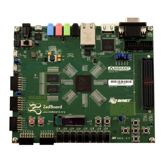
1 Introduction The ZedBoard is an evaluation and development board based on the Xilinx Zynq-7000 Extensible Processing Platform. Combining a dual Corex-A9 Processing System (PS) with 85,000 Series-7 Programmable Logic (PL) cells, the Zynq-7000 EPP can be targeted for broad use in many applications. - Page 5 HDMI transmitter HDMI Out VGA (12- 512Mbyte DDR3 bit color) DDR3 (x32) OLED 128x32 OLED Display PS_RST Reset DONE DONE LED PS_CLK 33Mhz PROG PROG GPIO/VP/VN XADC JTAG Primary JTAG Cont ZYNQ XC7Z020-CSG484 Figure 1 – ZedBoard Block Diagram 1-Aug-2012...
-
Page 6: Zynq Bank Pin Assignments
1.1 Zynq Bank Pin Assignments The following figure shows the Zynq bank pin assignments on the ZedBoard followed by a table that shows the detailed I/O connections. Figure 2 - Zynq Z7020 CSG484 Bank Assignments 1-Aug-2012... -
Page 7: Functional Description
2 Functional Description 2.1 EPP The ZedBoard features a Xilinx Zynq XC7Z020-1CSG484 EPP. The initial ZedBoards ship with Engineering Sample "CES" grade silicon. Later shipments will eventually switch to production "C" grade silicon once they become available. The EPP part markings indicate the silicon grade. - Page 8 ZedBoard these delay values can be recreated by following the directions found in the Excel worksheet. The PCB lengths are contained in the ZedBoard PCB trace length reports. The DQS to CLK Delay and Board Delay values are calculated specific to the ZedBoard memory interface PCB design.
- Page 9 In these memory use cases, the accuracy of the trace length info is more important. This is covered in further detail in section 10.6.8 of the Xilinx Zynq TRM, UG585. Figure 3 - DQS to Clock Delay Settings The Board Delay fields in the PS7 DDR Configuration window should be populated using the corresponding values from the table above.
-
Page 10: Spi Flash
20K pull-up resistor to 3.3V. This allows a QSPI clock frequency greater than FQSPICLK2. Note: Zynq only supports 24-bit addressing, however the full capacity of the 256Mb Flash can be accessed via internal bank switching. As of now the S25FL256S is not supported in iMPACT. - Page 11 Two packages can be used on the ZedBoard; SO-16 and WSON. For the WSON package, there is a heat sink slug under the package that is not connected to any signal on the PCB. Figure 5 - Overlying Packages for SPI Flash...
-
Page 12: Sd Card Interface
The Zynq PS SD/SDIO peripheral controls communication with the ZedBoard SD Card (A 4GB Class 4 card is included in the ZedBoard kit.) The SD card can be used for non-volatile external memory storage as well as booting the Zynq EPP. PS peripheral sd0 is connected through Bank 1/501 MIO[40-47], including, Card Detect and Write Protect. -
Page 13: Usb
The usb0 peripheral is used on the PS, connected through MIO[28-39] in MIO Bank 1/501. This USB port will not power the board. However, ZedBoard provides 5V when in Host or OTG modes. REFCLK pin of TUSB1210 is tied to ground as the EPP will drive the CLOCK input of this part. -
Page 14: Usb-Jtag
2.3.3 USB-JTAG The ZedBoard provides JTAG functionality based on the Digilent USB High Speed JTAG Module, SMT1 device. This USB-JTAG circuitry is fully supported and integrated into Xilinx ISE tools, including iMPACT, ChipScope, and SDK Debugger. Designers who want to re-use this circuit on their board can do so by acquiring these modules from Avnet. -
Page 15: Usb Circuit Protection
The ADV7511 supports both S/PDIF and 8-channel I2S audio. The S/PDIF can carry compressed audio including Dolby® Digital, DTS®, and THX®. There is an independent DPDIF input and output. The I2S interface is not connected on ZedBoard. Analog Devices offers Linux drivers and reference designs illustrating how to interface to this device. - Page 16 Table 7 - HDMI Interface Connections Signal Name Description Zynq EPP pin ADV7511 pin Hot Plug Detect signal input HD-INT Interrupt signal output HD-SCL I2C Interface. Supports CMOS AA18 logic levels from 1.8V to 3.3V HD-SDA HD-CLK Video Clock Input. Supports typical CMOS logic levels from 1.8V up to 3.3V...
- Page 17 Figure 9 - HDMI Video Interface Timing The HDMI transmitter connects externally via a HDMI Type A connector, J9, TE 1903015-1. Circuit protection for the HDMI interface is provided by a Tyco Electronics SESD0802Q4UG. 1-Aug-2012...
-
Page 18: Vga Connector
2.4.2 VGA Connector The ZedBoard also allows 12-bit color video output through a through-hole VGA connector, TE 1734682-2. Each color is created from resistor-ladder from four PL pins. Figure 10 - DB15 Table 8 - VGA Connections VGA Pin Signal... -
Page 19: I2S Audio Codec
Analog Devices provides Linux drivers for this device. http://www.analog.com/en/content/cu_over_sigmastudio_graphical_dev_tool_overview/fca.html The Codec interface to the EPP consists of the following connections: Table 9 - CODEC Connections Signal Name Description Zynq EPP pin ADAU1761 pin I2C Address Bit 0/SPI Latch AC-ADR0 Signal I2C Address Bit 1/SPI Data AC-ADR1... -
Page 20: Oled
The Zynq PS supports external power-on reset signals. The power-on reset is the master reset of the entire chip. This signal resets every register in the device capable of being reset. ZedBoard drives this signal from a comparator that holds the system in reset until all power supplies are valid. -
Page 21: Program Push Button Switch
2.7 User I/O 2.7.1 User Push Buttons The ZedBoard provides 7 user GPIO push buttons to the EPP; five on the PL-side and two on the PS-side. Pull-downs provide a known default state, pushing each button connects to Vcco. Table 12 - Push Button Connections... -
Page 22: User Leds
2.7.3 User LEDs The ZedBoard has eight user LEDs, LD0 – LD7. A logic high on the EPP I/O causes the LED to turn on. LED’s are sourced from 3.3V banks through 390Ω resistors. Table 14 - LED Connections Signal Name Zynq EPP pin 2.8 10/100/1000 Ethernet PHY... -
Page 23: Expansion Headers
2.9.1 LPC FMC Connector A single low-pin count (LPC) FMC slot is provided on the ZedBoard to support a large ecosystem of plug-in modules. The LPC FMC exposes 68 single-ended I/O, which can be configured as 34 differential pairs. The FMC interface spans over two PL I/O banks, banks 34 and 35. To meet the FMC spec, these banks are powered from an adjustable voltage set by jumper, J18. -
Page 24: Digilent Pmod™ Compatible Headers (2X6)
Digilent Pmod™ Compatible Headers (2x6) 2.9.2 The ZedBoard has five Digilent Pmod™ compatible headers (2x6). These are right-angle, 0.1” female headers that include eight user I/O plus 3.3V and ground signals as show in the figure below. Four Pmod connectors interface to the PL-side of the EPP. These will connect to EPP Bank 13 (3.3V). -
Page 25: Agile Mixed Signaling (Ams) Connector, J2
The ZedBoard AMS header is comparable with similar connectors on the Xilinx KC705 and ZC702 boards. Any AMS plug-in cards built for those boards should be compatible with ZedBoard as well. - Page 26 Figure 13 - Analog Header Pin out The following anti-aliasing filters were used for the XADC inputs: AUX0P AUX0N AUX8P AUX8N Figure 14 - Anti-Aliasing Filters for XADC Inputs 1-Aug-2012...
- Page 27 Table 17 - Analog Header Pin Out XADC Name Description Requirement EPP Pin Header Two pins required. Dedicated 1V peak-to- pins on the 7 series package. peak input XADC-VN-R : M12 This is the dedicated analog maximum XADC-VP-R : L11 input channel for the ADC(s).
-
Page 28: Configuration Modes
NOR, NAND, Quad-SPI, SD Card or JTAG. By default, the ZedBoard uses the SD Card configuration mode. The boot mode pins are MIO[8:2] and are used as follows: ... -
Page 29: Jtag
1.8V Expected configuration time using a 50MB/s QSPI flash is 250ms. PUDC_B is pulled high on ZedBoard but can be pulled low via JP5. This active-low input enables internal pull-ups during configuration on all SelectIO pins A push button labeled “PROG” is connected to the EPP PROG pin, T11, and pulled up. Pushing the button connects PROG to ground. -
Page 30: Power
ZedBoard power. 2.11.2 On/Off Switch ZedBoard includes an On/Off switch, SW8, to gate 12V. . When SW8 is in the OFF position, 12V is disconnected from the board. -
Page 31: Sequencing
2.11.4 Sequencing Sequencing for the power supplies follows the recommendations for the Zynq device. PS and PL INT and AUX supplies are tied together on the ZedBoard platform to create a low cost design. The following diagram illustrates the supply sequencing: 1V Vccint 1.8V XADC... -
Page 32: Power Good Led
PL Pmod #2 TE 5-534206-6 3000 PL Pmod #3 TE 5-534206-6 PL Pmod #4 TE 5-534206-6 FMC-LPC 2000 Total 1872 1035 2000 3814 2.11.7 Testing The power circuitry has been tested to verify compliance with the Zynq power requirements, such 1-Aug-2012... -
Page 33: Probes
Sequencing Verify sequencing responds as expected based on design Refer to Zynq Datasheet for the latest requirements 2.11.8 Probes Two ground test point are available on the board, J3 and J4. This allows easy access to attach ground leads of two scope probes to the board without having to locate GND pins on a header. -
Page 34: Zynq Epp Banks
Zynq EPP Banks The following figure and table show Zynq CLG484 I/O bank assignments on the Zynq board. Figure 19 - Zynq I/O Banks 1-Aug-2012... -
Page 35: Zynq Epp Bank Voltages
Selectable voltages include 1.8V, 2.5V and 3.3V. The 3.3V jumper was intentionally unpopulated on ZedBoard as these banks primarily connect to the FMC interface and many FMC cards are only 1.8V and 2.5V compatible. Connecting 3.3V to these cards can damage them, so leaving this jumper unpopulated reduces the risk of damaging FMC cards. -
Page 36: Jumper Settings
Open ups during configuration on all SelectIO pins. Install for SD Card PS_MIO0 Pull-Down Short boot on CES silicon. See Zynq Errata. JTAG Mode. GND cascades PS and PL GND – Cascaded Boot_Mode[3]/MIO[2] JTAG chains. VCC JTAG makes JTAG chains independent. - Page 37 Figure 20 - ZedBoard Jumper Map 1-Aug-2012...
-
Page 38: Mechanical
5 Mechanical The ZedBoard measures 6.3”x6.3”. Figure 21 - ZedBoard Mechanical 1-Aug-2012... - Page 39 Mouser Electronics Authorized Distributor Click to View Pricing, Inventory, Delivery & Lifecycle Information: Digilent 410-248P-KIT 410-248...
Need help?
Do you have a question about the ZedBoard and is the answer not in the manual?
Questions and answers