Advertisement
Quick Links
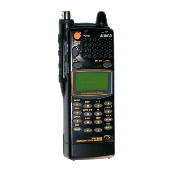
DJ-G5
CONTENTS
+ SPECIFICATIONS
+ CIRCUIT DESCRIPTION
1) Receiver System
2) Transmitter System
3) PLL Synthesizer Circuit
4) CPU and Peripheral Circuit
5) Terminal function of CPU
6) Terminal function of 4094
7) Frequency Table
+ SEMICONDUCTOR DATA
l) AK2341
2) BU4094BF
3) HD6433877
4) LC75366M
5) LC73881 M
6) M64076GP
7) MC3372VM
8) NJM21 00V
9) NJM2070M
10) RH5RH501A
11) RH5RH651A
12) S-80730SL-AT
13) S-AV28
14) S-AU57
15) S-81237SG-QE
16) TA75S01F
17) TA75W01FU
18) TC4W53F
19) TK10930VTL
20) uPD1 6430AGF-3B9
21) 24LC16B
22) Transistor, Diode and LED Outline Dra30
23) LCD Unit
+ EXPLODED VIEW
1) Charge Unit
2) RF Unit
3) IF Unit/CPU Unit
4) Front/Rear View
Service Manual
+ PARTS LIST
2
RF Unit
IF Unit
CPU Unit
3~5
SVV UniL
5
UVCO Unit
6
VVCO Unit
6~7
CHARGE Unit
10~12
PTT Unit
13
Mechanical Parts
13
+ ADJUSTMENT
14
1) Required Test Equipment
15
2) Adjustment for DJ-G5T/E
16
3) Adjustment Points
17
18
+ PC BOARD VIEW
19
20
1) RF Unit Side A
20
2) RF Unit Side B
21
3) IF Unit Side A
22
4) 1F Unit Side B
22
5) CPU Unit Side A
23
6) CPU Unit Side B
24
7) UVCO Unit
24
8) VVCO Unit
25
9) PTT Unit Side A
25
10) PTT Unit Side B
26
11) CHARGE Unit
26
12) SW Unit Side A
27
28
+ VOLTAGE TABLE
29
1) Diode
31~32
2) IC
3) Transistor
+ BLOCK DIAGRAM
33
34
35
+ SCHEMATIC DIAGRAM
36
1) RF Unit
2) IF Unit
3) CPU Unit
4) UVCO Unit
5) VVCO Unit
6) CHARGE Unit
7) PTT Unit
ALINCO INCORPORATED
TWIN 21 M.I.D. TOWER BUILDING 23F, 1-61, 2-CHOME,
SHIROMI CHUO-KU , OSAKA, 540-8580 JAPAN
Tel (81)6-6946-8150 fax (81)6-6946-8175
e-mail: export@alinco.co.jp
37~40
41~44
44~46
46
46
47
47
47
48
49
50
51
52
53
54
55
56
57
58
58
58
58
58
58
59~60
60~63
63~64
66~67
68~69
70~71
72~73
74
75
76
76
Advertisement

Related Manuals for Alinco DJ-G5


Summary of Contents for Alinco DJ-G5
- Page 1 DJ-G5 Service Manual CONTENTS + SPECIFICATIONS + PARTS LIST RF Unit 37~40 IF Unit 41~44 + CIRCUIT DESCRIPTION CPU Unit 44~46 1) Receiver System SVV UniL 2) Transmitter System UVCO Unit 3) PLL Synthesizer Circuit VVCO Unit 4) CPU and Peripheral Circuit...
- Page 2 General 108.000~173.995 420.000~479.995 DJ-G5T L-band (AM FM) (FM) 1 30.000~l 73.995 Receiver range(MHz) R-band (FM) DJ-G5E 144.000~145.995 430.000~439.995 Transmitter range(M DJ-G5T 144.000~147.995 438.000~449.995 DJ-G5E 144.000~145.995 430.000~439.995 Modulation F2E.,F3E(FM) Antenna impedance 50 ohm Operating temperature range -10 ~ +60*C Supply voltage (rated voltage) External (V) 4.5~16.0(13.8) Ni-Cd(V) 4.5~16.0(4.8)
- Page 3 CIRCUIT DESCRIPTTON 1) Receiver System The receiver system is the double-conversion superheterodyne. ln L band the first IF is 38.9MHz and second IF is 455kHz, and in R band the first IF is 45.1MHz and second IF is 455kHz. 1 Front End 1-1 108.00MHz~ 173.995MHz (144M Band Main) The receiving signal is passed through the low-pass filter (L90, L91 , L92, C220, C229, C230, C231, C235), and amplified in RF amplifier (Q77), then led to the...
- Page 4 3 Demodulation 3-1 L Band After amplified in the first IF amplifier (Q78), the signal is fed to the demodulation IC (IC302) Pin24. The first IF signal outputted to Pin24 (38.9MHz) is mixed in the mixer of IC302 with the local signal of 38.455MHz which is oscillated in the oscillation circuit of IC302 and the crystal oscillator (X303), then converted into the second IF signal of 455kHz.
- Page 5 5-2 R Band A part of the audio signal of IC301 Ping is selected and amplified by the noise amplifiers in R316, R317, R318, R319, C318, C319, C320, and IC301. Then it is supplied from IC301 Pin11 to be amplified again in the noise amplifier (Q303). The amplified noise factor is rectified in D301 , adjusted the level in VR30l , and applied to CPU (IC508) Pin97, then converted to the dligital signal.
- Page 6 3) PLL Synthesizer Circuit 1 PLL The data is sent to the PLL IC (IC53) Pin2 and the clock is sent to Pin3 from CPU (IC508), then the ratio of the division is decided each in L band and R band. Each VCO oscillating signal is amplified in the buffer (Q73: L band, Q66: R band), and the signal in L band is applied to Pin15, then the signal in R band is applied to Pin6.
- Page 7 2 Display Lamp Circuit The regulated power supply circuit consisting of Q505, Q507, R508, R509 supplies H from CPU (IC508) when LAMP key is pressed. Then it is applied to the base of Q507, and the voltage of 3.5V is outputted from the collector of Q505. lt is fed to each LED (D503~D506, D509,D511 ,D513,D514).
- Page 8 5) Terminal function of CPU Name Pin Name Description 1 ANO Analog lN Power supply voltage detection 2 AVSS Analogground 3 TEST Connect to ground 4 X2 OPEN Open when not used 5 X1 Power supply 6 VSS Ground 7 OSC1 OSC1 Internal oscillator input 8 OSC2...
- Page 9 Name Pin Name Description 51 P67 KIN4 Key matrix input4 52 P70 KOT1 Key matrix output1 53 P71 KOT2 Key matrix output2 54 P72 KOT3 Key matrix output3 55 P73 KOT4 Key matrix output4 56 P74 PRST Normal Pulse PLL reset pulse input judgement 57 P75 Normal EEPROM data...
- Page 10 6) Terminal function of 4094 4094 po Port Name Function Logic Description TIME UHF high power control Active Low Low power UMlD UHF middle power control Active Low UHF middle=H H VHF high power control Active Low Low power VMID VHF middle power control Active Low VHF middle=H H VATTC VHF RX attenuater control Active Low ATT ON...
- Page 13 (XA0505)
- Page 40 ADJUSTMENT 1) Required Test Equipment 10. Distortion Meter/SINAD Meter 1. Regulated Power Supply Measurable frequency: 1kHz Supply voltage: DC 13.8V Input level: Up to 40dB Current: 3A or more Distortion level: 1 % ~1 00% 2. Digital Multimeter 11. Frequency Counter Voltage range: FS =20V or so Measurable frequency: Up to 500MHz...
- Page 41 2) Adjustment for DJ-G5TIE Item Condition Measurement Adjustment Specifications TX/RX Equipment Unit Unit Pans Method Reference L band Digital V-VCO Voltage f=l45.05MHz Multimeter V-VCO L701 3.7V 3.7V+/-0.1V R band Digital U-VCO f=435.05MHz Multimeter U-VCO L601 1.2V 1.2V+/-0.1V R band Reference f=435.05MHz (E) Freq.
- Page 49 UU0026 UU0026...
- Page 50 VOLTAGE TABLE 1) Diode 3 Note 3.57 3.57 UHF LOW TX 3.57 3.57 VHF LOW TX 0.03 0.03 UHF LOW TX 1.21 1.85 0 R:433.00MHz 3.36 4.14 VHF TX 2.66 3.47 L:433.00MHz 1.04 1.86 0 L:433.00MHz 2.76 L:144,00MHz 0.91 0.91 VHF LOW TX Anode Cathode Note 1.69...
- Page 51 3 Note D516 0.24 3.46 PTT:ON D516 D516 Anode Cathode Note D601 1.25 D602 1.68 D603 1.68 D604 3.11 R:SUB D605 3.11 R:SUB Anode Cathode Note D701 1.22 D702 4.34 D703 4.34 D704 2.2 L:SUB D705 2.2 L:SUB Anode Cathode D801 13.57 13.57...
- Page 52 lC303 PinNo. Voltage Note PinNo. Voltage Note 0.86 3.39 AM 0.01 0.00 0.00 0.86 0.00 3.56 IC304 IC306 PinNo. Voltage PinNo. Voltage PinNo. Voltage PinNo. Voltage 2.50 2.51 2.52 2.48 0.00 0.00 2.51 2.50 2.50 2.48 2.36 2.50 2.50 2.50 0.00 5.00 2.50...
- Page 53 IC501 IC504 TSQ..ON PinNo. Voltage PinNo. Voltage PinNo. Voltage Pin No. Voltage 0.95 3.45 1.72 1.48 1.16 2.16 0.98 3.41 3.53 1.25 1.88 1.72 1.72 1.72 1.72 IC502 DSQ:ON 3.45 1.72 PinNo. Voltage Pin No. Voltage 1.68 2.22 1.71 1.73 1.72 1.72 1.72...
- Page 54 IC52 PinNo. Voltage PinNo. Voltage IC841 PinNo. Voltage PinNo. Voltage 3.49 0.09 3.57 0.09 3.57 3.57 3.52 3.57 3.57 3.57 l5 3.57 L: 145.00MHz LOW POWER 3.57 R: 433.00MHz LOW POWER IC53 PinNo. Voltage PinNo. Voltage PinNo. Voltage PinNo. Voltage 3.56 1.65 1.72...
- Page 55 1.00 3.00 5 Note Q302 12.98 13.53 3.24 2.70 3.25 Q319 13.01 13.58 3.39 2.91 3.52 When receiving Q326 3.46 0.00 0.20 3.57 3.58 L:VHF,R:UHF Q328 3.47 0.00 0.10 3.57 3.58 L:VHF,R:UHF Q329 3.50 3.50 0.00 3.57 0.00 Drain Gate Source Q307 1.03...
Need help?
Do you have a question about the DJ-G5 and is the answer not in the manual?
Questions and answers