Table of Contents
Advertisement
Quick Links
www.ti.com
LOW-POWER DC/DC BOOST CONVERTER IN SOT-23 AND SON PACKAGES
FEATURES
1
•
1.8-V to 6-V Input Voltage Range
•
Adjustable Output Voltage Range up to 28 V
•
400-mA (TPS61040) and 250-mA (TPS61041)
Internal Switch Current
•
Up to 1-MHz Switching Frequency
•
28-mA Typical No-Load Quiescent Current
•
1-mA Typical Shutdown Current
•
Internal Soft Start
•
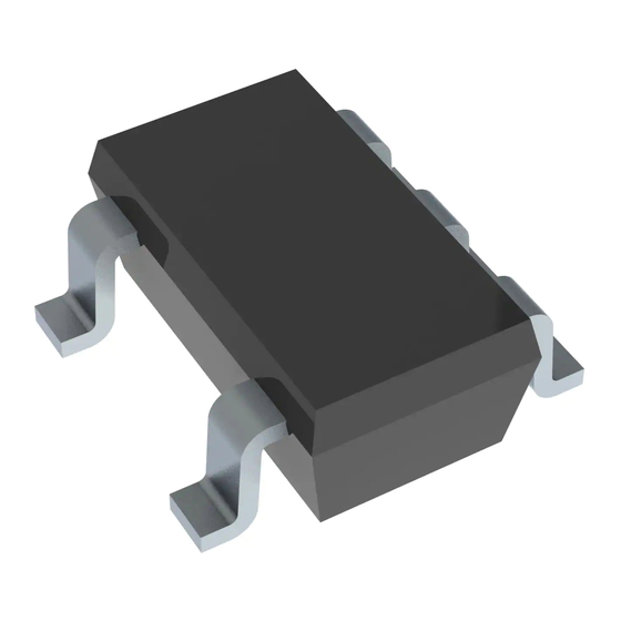
Available in SOT23-5, TSOT23-5,
and 2 × 2 × 0.8-mm SON Packages
APPLICATIONS
•
LCD Bias Supply
•
White-LED Supply for LCD Backlights
•
Digital Still Camera
•
PDAs, Organizers, and Handheld PCs
•
Cellular Phones
•
Internet Audio Player
•
Standard 3.3-V/5-V to 12-V Conversion
TYPICAL APPLICATION
L1
10 µH
V
IN
1.8 V to 6 V
5
V
IN
C
IN
4.7 µF
4
EN
1
Please be aware that an important notice concerning availability, standard warranty, and use in critical applications of Texas
Instruments semiconductor products and disclaimers thereto appears at the end of this data sheet.
PRODUCTION DATA information is current as of publication date.
Products conform to specifications per the terms of the Texas
Instruments standard warranty. Production processing does not
necessarily include testing of all parameters.
Check for Samples: TPS61040,
D1
C
R1
1
SW
3
FB
2
GND
R2
SLVS413F – OCTOBER 2002 – REVISED DECEMBER 2010
TPS61041
DESCRIPTION
The
TPS61040/41
converter dedicated for small to medium LCD bias
supply and white LED backlight supplies. The device
is ideal to generate output voltages up to 28 V from a
dual cell NiMH/NiCd or a single cell Li-Ion battery.
The part can also be used to generate standard
3.3-V/5-V to 12-V power conversions.
The
TPS61040/41
frequency up to 1 MHz. This allows the use of small
external components using ceramic as well as
tantalum output capacitors. Together with the thin
SON package, the TPS61040/41 gives a very small
overall solution size. The TPS61040 has an internal
400 mA switch current limit, while the TPS61041 has
a 250-mA switch current limit, offering lower output
voltage ripple and allows the use of a smaller form
factor inductor for lower power applications. The low
quiescent current (typically 28 mA) together with an
optimized control scheme, allows device operation at
very high efficiencies over the entire load current
range.
DDC, DBV PACKAGE
(Top View)
1
SW
GND
2
3
FB
V
OUT
V
to 28 V
IN
FF
C
O
1 µF
Copyright © 2002–2010, Texas Instruments Incorporated
is
a
high-frequency
operates
with
DRV PACKAGE
(Top View)
GND
5
V
1
IN
V
2
IN
EN
3
4
EN
EFFICIENCY
vs
OUTPUT CURRENT
90
V
= 18 V
O
88
V
= 5 V
I
86
84
V
= 3.6 V
I
82
80
V
= 2.4 V
I
78
76
74
72
70
0.1
1
I
− Output Current − mA
O
TPS61040
TPS61041
boost
a
switching
SW
6
NC
5
4
FB
10
100
Advertisement
Table of Contents

Related Manuals for Texas Instruments TPS61041


Summary of Contents for Texas Instruments TPS61041
-
Page 1: Typical Application
2 × 2 × 0.8-mm SON Packages SON package, the TPS61040/41 gives a very small overall solution size. The TPS61040 has an internal APPLICATIONS 400 mA switch current limit, while the TPS61041 has • LCD Bias Supply a 250-mA switch current limit, offering lower output voltage ripple and allows the use of a smaller form •... - Page 2 SLVS413F – OCTOBER 2002 – REVISED DECEMBER 2010 www.ti.com This integrated circuit can be damaged by ESD. Texas Instruments recommends that all integrated circuits be handled with appropriate precautions. Failure to observe proper handling and installation procedures can cause damage.
-
Page 3: Detailed Description
The higher the input voltage and the lower the inductor value, the greater the peak. By selecting the TPS61040 or TPS61041, it is possible to tailor the design to the specific application current limit requirements. A lower current limit supports applications requiring lower output power and allows the use of an inductor with a lower current rating and a smaller form factor. - Page 4 POWER RATING POWER RATING = 25°C 250°C/W 357 mW 3.5 mW/°C 192 mW 140 mW DDC, DRV 76°C/W 1300 mW 13 mW/°C 688 mW 500 mW Submit Documentation Feedback Copyright © 2002–2010, Texas Instruments Incorporated Product Folder Link(s): TPS61040 TPS61041...
-
Page 5: Recommended Operating Conditions
= 18 V; 0 mA ≤ I ≤ 30 mA 0.15 %/mA (1) The line and load regulation depend on the external component selection. See the application section for further information. Submit Documentation Feedback Copyright © 2002–2010, Texas Instruments Incorporated Product Folder Link(s): TPS61040 TPS61041... -
Page 6: Typical Characteristics
= 18 V = 5 V TPS61040 = 3.6 V TPS61041 = 2.4 V − Output Current − mA − Load Current − mA Figure 1. Figure 2. Submit Documentation Feedback Copyright © 2002–2010, Texas Instruments Incorporated Product Folder Link(s): TPS61040 TPS61041... - Page 7 = 27°C 1.236 = −40°C = 2.4 V 1.234 1.232 1.23 −40 −20 − Temperature − °C − Input Voltage − V Figure 5. Figure 6. Submit Documentation Feedback Copyright © 2002–2010, Texas Instruments Incorporated Product Folder Link(s): TPS61040 TPS61041...
- Page 8 −40 −30 −20 −10 0 10 20 30 40 50 60 70 80 90 − Temperature − °C − Supply Voltage − V Figure 9. Figure 10. Submit Documentation Feedback Copyright © 2002–2010, Texas Instruments Incorporated Product Folder Link(s): TPS61040 TPS61041...
- Page 9 = 18 V 100 mA/div 5 V/div 1 V/div 1 mA to 10 mA 50 mA/div 200 µS/div Figure 13. Load Transient Response Figure 14. Start-Up Behavior Submit Documentation Feedback Copyright © 2002–2010, Texas Instruments Incorporated Product Folder Link(s): TPS61040 TPS61041...
- Page 10 = Peak current as described in the Peak Current Control section L = Selected inductor value = Maximum switching frequency as calculated previously h = Expected converter efficiency. Typically 70% to 85% Submit Documentation Feedback Copyright © 2002–2010, Texas Instruments Incorporated Product Folder Link(s): TPS61040 TPS61041...
-
Page 11: Setting The Output Voltage
= Switching frequency of the converter at the nominal load current (See the Inductor Selection, Maximum Load Current section for calculating the switching frequency) = Choose a value that comes closest to the result of the calculation Submit Documentation Feedback Copyright © 2002–2010, Texas Instruments Incorporated Product Folder Link(s): TPS61040 TPS61041... -
Page 12: Line And Load Regulation
6.3 V Tayo Yuden JMK212BJ106MG TPS61040/41 1 mF/X7R/1206 25 V Tayo Yuden TMK316BJ105KL 1 mF/X5R/1206 35 V Tayo Yuden GMK316BJ105KL 4.7 mF/X5R/1210 25 V Tayo Yuden TMK325BJ475MG Submit Documentation Feedback Copyright © 2002–2010, Texas Instruments Incorporated Product Folder Link(s): TPS61040 TPS61041... -
Page 13: Input Capacitor Selection
Wide traces should be used for connections in bold as shown in Figure 15. A star ground connection or ground plane minimizes ground shifts and noise. Figure 15. Layout Diagram Submit Documentation Feedback Copyright © 2002–2010, Texas Instruments Incorporated Product Folder Link(s): TPS61040 TPS61041... - Page 14 1 µF 0.1 µF (Optional) 4.7 µF Sumida CR32-100 160 kW Motorola MBR0530 Tayo Yuden JMK212BY475MG Tayo Yuden TMK316BJ105KL Figure 18. LCD Bias Supply With Load Disconnect Submit Documentation Feedback Copyright © 2002–2010, Texas Instruments Incorporated Product Folder Link(s): TPS61040 TPS61041...
- Page 15 Tayo Yuden JMK212BY475MG Figure 21. Dual Battery Cell to 5-V/50-mA Conversion Efficiency Approx. Equals 84% at V = 2.4 V to Vo = 5 V/45 mA Submit Documentation Feedback Copyright © 2002–2010, Texas Instruments Incorporated Product Folder Link(s): TPS61040 TPS61041...
- Page 16 A smaller output capacitor value for C2 causes a larger LED ripple. Figure 23. White LED Supply With Adjustable Brightness Control Using an Analog Signal on the Feedback Pin Submit Documentation Feedback Copyright © 2002–2010, Texas Instruments Incorporated Product Folder Link(s): TPS61040 TPS61041...
- Page 17 PACKAGE OPTION ADDENDUM www.ti.com 17-May-2014 PACKAGING INFORMATION Orderable Device Status Package Type Package Pins Package Eco Plan Lead/Ball Finish MSL Peak Temp Op Temp (°C) Device Marking Samples Drawing (4/5) TPS61040DBVR ACTIVE SOT-23 3000 Green (RoHS CU NIPDAU Level-1-260C-UNLIM -40 to 85 PHOI &...
- Page 18 In no event shall TI's liability arising out of such information exceed the total purchase price of the TI part(s) at issue in this document sold by TI to Customer on an annual basis. OTHER QUALIFIED VERSIONS OF TPS61040, TPS61041 : •...
-
Page 19: Tape And Reel Information
PACKAGE MATERIALS INFORMATION www.ti.com 28-Nov-2013 TAPE AND REEL INFORMATION *All dimensions are nominal Device Package Package Pins Reel Reel Pin1 Type Drawing Diameter Width (mm) (mm) (mm) (mm) (mm) Quadrant (mm) W1 (mm) TPS61040DBVR SOT-23 3000 178.0 3.23 3.17 1.37 TPS61040DBVR SOT-23 3000... - Page 20 PACKAGE MATERIALS INFORMATION www.ti.com 28-Nov-2013 *All dimensions are nominal Device Package Type Package Drawing Pins Length (mm) Width (mm) Height (mm) TPS61040DBVR SOT-23 3000 180.0 180.0 18.0 TPS61040DBVR SOT-23 3000 203.0 203.0 35.0 TPS61040DDCR 3000 195.0 200.0 45.0 TPS61040DDCT 195.0 200.0 45.0 TPS61040DRVR...
-
Page 27: Important Notice
IMPORTANT NOTICE Texas Instruments Incorporated and its subsidiaries (TI) reserve the right to make corrections, enhancements, improvements and other changes to its semiconductor products and services per JESD46, latest issue, and to discontinue any product or service per JESD48, latest issue.
Need help?
Do you have a question about the TPS61041 and is the answer not in the manual?
Questions and answers