Table of Contents
Advertisement
Quick Links
Advertisement
Table of Contents

Related Manuals for Terasic De1-Soc


Summary of Contents for Terasic De1-Soc
-
Page 2: Table Of Contents
..............................3 ACKAGE ONTENTS 1.2 DE1-S CD .............................. 4 YSTEM 1.3 G ................................4 ETTING CHAPTER 2 INTRODUCTION OF THE DE1-SOC BOARD ................. 5 2.1 L ............................5 AYOUT AND OMPONENTS 2.2 B DE1-S ......................7 LOCK IAGRAM OF THE... - Page 3 3.7.7 2- USB H ............................... 49 PORT 3.7.8 G-S ................................50 ENSOR 3.7.9 LTC C ..............................51 ONNECTOR CHAPTER 4 DE1-SOC SYSTEM BUILDER ......................53 4.1 I ............................... 53 NTRODUCTION 4.2 G ............................53 ENERAL ESIGN 4.3 U DE1-S ........................54...
-
Page 4: Chapter 1 De1-Soc Development Kit
DE1-SoC Development Kit The DE1-SoC Development Kit presents a robust hardware design platform built around the Altera System-on-Chip (SoC) FPGA, which combines the latest dual-core Cortex-A9 embedded cores with industry-leading programmable logic for ultimate design flexibility. Users can now leverage the power of tremendous re-configurability paired with a high-performance, low-power processor system. -
Page 5: De1-S O C System Cd
DE1-SoC System CD-ROM 12V DC power adapter The DE1-SoC System CD containing the DE1-SoC documentation and supporting materials, including the User Manual, System Builder, reference designs and device datasheets. User can download this System CD form the link : http://de1-soc.terasic.com. -
Page 6: Introduction Of The De1-Soc Board
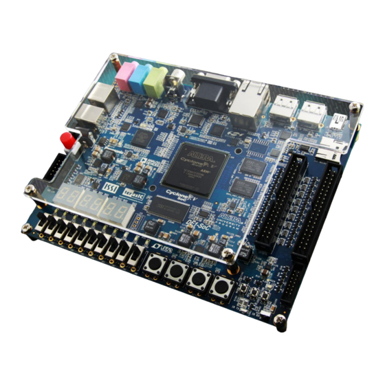
Chapter 2 Introduction of the DE1-SoC Board This chapter presents the features and design characteristics of the board. A photograph of the board is shown in Figure 2-1. It depicts the layout of the board and indicates the location of the connectors and key components. - Page 7 Figure 2-2 Development Board (bottom view) The DE1-SoC board has many features that allow users to implement a wide range of designed circuits, from simple circuits to various multimedia projects. The following hardware is provided on the board: FPGA ...
-
Page 8: Block Diagram Of The De1-S O C Board
HPS (Hard Processor System) 800MHz Dual-core ARM Cortex-A9 MPCore processor 1GB DDR3 SDRAM (32-bit data bus) 1 Gigabit Ethernet PHY with RJ45 connector 2-port USB Host, Normal Type-A USB connector Micro SD card socket ... - Page 9 Following is more detailed information about the blocks in Figure 2-3: Cyclone V SoC 5CSEMA5F31 Device Dual-core ARM Cortex-A9 (HPS) 85K Programmable Logic Elements 4,450 Kbits embedded memory 6 Fractional PLLs 2 Hard Memory Controllers ...
- Page 10 24-bit VGA DAC 24-bit CODEC, Line-in, line-out, and microphone-in jacks TV Decoder (NTSC/PAL/SECAM) and TV-in connector 5 User Keys (FPGA x4, HPS x1) 10 User switches (FPGA x10) 11 User LEDs (FPGA x10, HPS x 1) ...
-
Page 11: Using The De1-Soc Board
Chapter 3 Using the DE1-SoC Board This chapter gives instructions for using the board and describes each of its peripherals. This section will explain the settings of FPGA configuration modes, HPS boot source select and HPS flash controller clock frequency in detail. -
Page 12: Hps Bootsel And Clksel Setting
Fast 10000 Enabled/ Disabled Disabled Standard 10001 Fast 10010 AS(X1 and X4) Enabled/ Disabled Enabled Standard 10011 Table 3-2 shows the switch controls and descriptions for MSEL. Table 3-2 SW10 FPGA Configuration Mode Switch Board Reference Signal Name Description Default SW10.1 MSEL0 SW10.2... - Page 13 1.8 V SD/MMC Flash memory(*1) 3.0 V SD/MMC Flash memory 1.8 V SPI or quad SPI Flash memory(*1) 3.0 V SPI or quad SPI Flash memory (*1) : Not supported on DE1-SoC board Table 3-4 SD/MMC Controller CSEL Pin Settings CSEL Pin Setting...
-
Page 14: Configuring The Cyclonev S O C Fpga
DE1-SoC board is turned off. When the board’s power is turned on, the configuration data in the EPCQ256 device is automatically loaded into the Cyclone V SoC FPGA. - Page 15 Configuring the FPGA in JTAG Mode There are two devices (FPGA and HPS) on the JTAG Chain, the configure flow is different from DE1. The following shows the programming flow with JTAG mode step by step. Open Programmer and click “Auto Detect “ as Figure 3-2 Figure 3-2 FPGA JTAG Programming Steps 1 ...
- Page 16 Both FPGA and HPS will be detected as Figure 3-4 Figure 3-4 FPGA JTAG Programming Steps 3 Click the FPGA device, right click mouse to popup the manual, and then select .sof file for FPGA as Figure 3-5...
- Page 17 Figure 3-5 FPGA JTAG Programming Steps 4 Select .sof file for FPGA as Figure 3-6 Figure 3-6 FPGA JTAG Programming Steps 5...
- Page 18 Click “Program/Configure” check box, and then click “Start” button to download .sof file into FPGA as Figure 3-7 Figure 3-7 FPGA JTAG Programming Steps 6 Configuring the FPGA in AS Mode (from EPCQ256) The board contains a quad serial configuration device (EPCQ256) that stores configuration data for the Cyclone V SoC FPGA.
-
Page 19: Board Status Elements
FPGA-based SFL is a soft intellectual property (IP) core within the FPGA that bridges the JTAG and flash interfaces. The SFL mega-function is available from Quartus II software. Figure 3-8 shows the programming method when adopting a SFL solution Please refer to Chapter 9: Steps of Programming the Quad Serial Configuration Device for the basic programming instruction on the serial configuration device Figure 3-8 Programming a Quad Serial Configuration Device with the SFL Solution The board includes status LEDs. -
Page 20: Board Reset Elements
The board equips two HPS reset circuits (See Figure 3-9). Table 3-7 shows the buttons references and its descriptions. Figure 3-10 shows the reset tree on the board. Figure 3-9 Board Reset Elements Table 3-7 Reset Elements Board Reference Signal Name Description Cold reset to the HPS , Ethernet PHY and USB host device . -
Page 21: Clock Circuitry
Figure 3-10 Reset Tree on the Development Board Figure 3-11 is a diagram showing the default frequencies of all of the external clocks going to the Cyclone V SoC FPGA. A clock generator is used to distribute clock signals with low jitter to FPGA. The four distributing 50MHz clock signals are connected to the FPGA that are used for clocking the user logic. -
Page 22: Interface On Fpga
Figure 3-11 Block diagram of the clock distribution Table 3-8 Pin Assignments for Clock Inputs Signal Name FPGA Pin No. Description I/O Standard CLOCK_50 PIN_AF14 50 MHz clock input 3.3V CLOCK2_50 PIN_AA16 50 MHz clock input 3.3V CLOCK3_50 PIN_Y26 50 MHz clock input 3.3V CLOCK4_50 PIN_K14... -
Page 23: User Push-Buttons, Switches And Leds On Fpga
3.6.1 User Push-buttons, Switches and LEDs on FPGA The board provides four push-button switches connected to FPGA as shown in Figure 3-12 . Each of these switches is debounced Connections between the push-button and Cyclone V SoC FPGA using a Schmitt Trigger circuit, as indicated in Figure 3-13. - Page 24 There are ten slide switches connected to FPGA on the board (See Figure 3-14). These switches are not debounced, and are assumed for use as level-sensitive data inputs to a circuit. Each switch is connected directly to a pin on the Cyclone V SoC FPGA. When the switch is in the DOWN position (closest to the edge of the board), it provides a low logic level to the FPGA, and when the switch is in the UP position it provides a high logic level.
- Page 25 Figure 3-15 Connections between the LEDs and Cyclone V SoC FPGA Table 3-9 Pin Assignments for Slide Switches Signal Name FPGA Pin No. Description I/O Standard SW[0] PIN_AB12 Slide Switch[0] 3.3V SW[1] PIN_AC12 Slide Switch[1] 3.3V SW[2] PIN_AF9 Slide Switch[2] 3.3V SW[3] PIN_AF10...
-
Page 26: Using The 7-Segment Displays
3.3V 3.6.2 Using the 7-segment Displays The DE1-SoC board has six 7-segment displays. These displays are arranged into three pairs, behaving the intent of displaying numbers of various sizes. As indicated in the schematic in Figure 3-16, the seven segments (common anode) are connected to pins on Cyclone V SoC FPGA. - Page 27 HEX0[1] PIN_AE27 Seven Segment Digit 0[1] 3.3V HEX0[2] PIN_AE28 Seven Segment Digit 0[2] 3.3V HEX0[3] PIN_AG27 Seven Segment Digit 0[3] 3.3V HEX0[4] PIN_AF28 Seven Segment Digit 0[4] 3.3V HEX0[5] PIN_AG28 Seven Segment Digit 0[5] 3.3V HEX0[6] PIN_AH28 Seven Segment Digit 0[6] 3.3V HEX1[0] PIN_AJ29...
- Page 28 3.6.3 Using the 2x20 GPIO Expansion Headers The Board provides two 40-pin expansion headers. The header connects directly to 36 pins of the Cyclone V SoC FPGA, and also provides DC +5V (VCC5), DC +3.3V (VCC3P3), and two GND pins. The maximum power consumption of the daughter card that connects to GPIO port is shown Table 3-13.
- Page 29 GPIO_0 [4] PIN_AK16 GPIO Connection 0[4] 3.3V GPIO_0 [5] PIN_AK18 GPIO Connection 0[5] 3.3V GPIO_0 [6] PIN_AK19 GPIO Connection 0[6] 3.3V GPIO_0 [7] PIN_AJ19 GPIO Connection 0[7] 3.3V GPIO_0 [8] PIN_AJ17 GPIO Connection 0[8] 3.3V GPIO_0 [9] PIN_AJ16 GPIO Connection 0[9] 3.3V GPIO_0 [10] PIN_AH18...
-
Page 30: Using The 24-Bit Audio Codec
3.6.4 Using the 24-bit Audio CODEC The DE1-SoC board provides high-quality 24-bit audio via the Wolfson WM8731 audio CODEC (Encoder/Decoder). This chip supports microphone-in, line-in, and line-out ports, with a sample rate adjustable from 8 kHz to 96 kHz. The WM8731 is controlled via by a serial I2C bus, which is connected to HPS or Cyclone V SoC FPGA through a I2C multiplexer. - Page 31 I2C Data 3.3V 3.6.5 I2C Multiplexer The DE1-SoC board implements an I2C multiplexer so that HPS can access the I2C bus originally owned by FPGA. Figure 3-19 shows the connection of I2C multiplexer. HPS will own I2C bus and then can access Audio CODEC and TV Decoder when the HPS_I2C_CONTROL signal is set to high.
-
Page 32: I2C Multiplexer 3.6.6 Vga
3.3V 3.6.6 The DE1-SoC board includes a 15-pin D-SUB connector for VGA output. The VGA synchronization signals are provided directly from the Cyclone V SoC FPGA, and the Analog Devices ADV7123 triple 10-bit high-speed video DAC (only the higher 8-bits are used) is used to produce the analog data signals (red, green, and blue). - Page 33 Detailed information for using the ADV7123 video DAC is available in its datasheet, which can be found on the manufacturer’s website, or in the Datasheets\VIDEO DAC folder on the DE1-SoC System CD. The pin assignments between the Cyclone V SoC FPGA and the ADV7123 are listed in...
- Page 34 Figure 3-21 VGA horizontal timing specification Table 3-17 VGA Horizontal Timing Specification VGA mode Horizontal Timing Spec Configuration Resolution(HxV) a(us) b(us) c(us) d(us) Pixel clock(MHz) VGA(60Hz) 640x480 25.4 VGA(85Hz) 640x480 17.8 SVGA(60Hz) 800x600 SVGA(75Hz) 800x600 16.2 SVGA(85Hz) 800x600 14.2 XGA(60Hz) 1024x768 15.8 XGA(70Hz)
-
Page 35: Tv Decoder
3.6.7 TV Decoder The DE1-SoC board is equipped with an Analog Device ADV7180 TV decoder chip. The ADV7180 is an integrated video decoder that automatically detects and converts a standard analog baseband television signals (NTSC, PAL, and SECAM) into 4:2:2 component video data compatible with the 8-bit ITU-R BT.656 interface standard. - Page 36 The registers in the TV decoder can be programmed by a serial I2C bus, which is connected to HPS or Cyclone V SoC FPGA through a I2C multiplexer as indicated in Figure 3-22. Note that the I2C address W/R of the TV decoder (U4) is 0x40/0x41. The pin assignments are listed in Table 3-20.
-
Page 37: Ir Receiver
The board provides an infrared remote-control receiver module (model: IRM-V538/TR1), whose datasheet is offered in the Datasheets\ IR Receiver and Emitter folder on DE1-SoC System CD. The accompanied remote controller with an encoding chip of uPD6121G is very suitable of generating expected infrared signals. -
Page 38: Sdram Memory On Fpga
Figure 3-24 Connection between FPGA and IR Emitter LED Table 3-22 Pin Assignments for IR Signal Name FPGA Pin No. Description I/O Standard IRDA_TXD PIN_ AB30 IR Emitter 3.3V 3.6.10 SDRAM Memory on FPGA The board features 64MB of SDRAM, implemented using a 64MB (32Mx16) SDRAM device. The device consists of 16-bit data line, control line and address line connected to the FPGA. - Page 39 Figure 3-25 Connections between FPGA and SDRAM Table 3-23 SDRAM Pin Assignments Signal Name FPGA Pin No. Description I/O Standard DRAM_ADDR[0] PIN_AK14 SDRAM Address[0] 3.3V DRAM_ADDR[1] PIN_AH14 SDRAM Address[1] 3.3V DRAM_ADDR[2] PIN_AG15 SDRAM Address[2] 3.3V DRAM_ADDR[3] PIN_AE14 SDRAM Address[3] 3.3V DRAM_ADDR[4] PIN_AB15 SDRAM Address[4]...
-
Page 40: Ps/2 Serial Port
SDRAM Chip Select 3.3V 3.6.11 PS/2 Serial Port The DE1-SoC board includes a standard PS/2 interface and a connector for a PS/2 keyboard or mouse. Figure 3-26 shows the schematic of the PS/2 circuit. In addition, users can use the PS/2... - Page 41 Figure 3-26 Connection between FPGA and PS/2 Figure 3-27 Y-Cable use for both Keyboard and Mouse Table 3-24 PS/2 Pin Assignments Signal Name FPGA Pin No. Description I/O Standard PS2_CLK PIN_AD7 PS/2 Clock 3.3V PS2_DAT PIN_AE7 PS/2 Data 3.3V PS2_CLK2 PIN_AD9 PS/2 Clock (reserved for second PS/2 device) 3.3V...
-
Page 42: A/D Converter And 2X5 Header
3.6.12 A/D Converter and 2x5 Header The DE1-SoC contains an AD7928 lower power, eight-channel CMOS 12-bit analog-to-digital converter. This A-to-D provides conversion throughput rates up to 1MSPS. It can be configured to accept eight input signals at inputs ADC_IN0 through ADC_IN7. This eight input signals are... -
Page 43: Interface On Hard Processor System (Hps)
Figure 3-29 Wiring for 2x5 header and A/D converter Table 3-25 Pin Assignments for ADC Signal Name FPGA Pin No. Description I/O Standard ADC_CS_N PIN_AJ4 Chip select 3.3V ADC_DOUT PIN_AK3 Digital data input 3.3V ADC_DIN PIN_AK4 Digital data output 3.3V ADC_SCLK PIN_AK2 Digital clock input... -
Page 44: Gigabit Ethernet
Table 3-26 Pin Assignments for LEDs, Switches and Buttons Signal Name HPS GPIO Register/bit Function HPS_KEY GPIO54 GPIO1[25] HPS_LED GPIO53 GPIO1[24] The board provides Ethernet support via an external Micrel KSZ9021RN PHY chip and HPS Ethernet MAC function. The KSZ9021RN chip with integrated 10/100/1000 Mbps Gigabit Ethernet transceiver support RGMII MAC interfaces. -
Page 45: Uart
FT232R chip and connects to the host using an USB Mini-B connector. For detailed information on how to use the transceiver, please refer to the datasheet, which is available on the manufacturer’s website, or in the Datasheets\UART TO USB folder on the DE1-SoC System Figure 3-31... -
Page 46: Ddr3 Memory On Hps
Figure 3-31 Connections between the Cyclone V SoC FPGA and FT232R Chip Table 3-29 UART Interface I/O Signal Name FPGA Pin No. Description I/O Standard HPS_UART_RX PIN_B25 HPS UART Receiver 3.3V HPS_UART_TX PIN_C25 HPS UART Transmitter 3.3V HPS_CONV_USB_N PIN_B15 Reserve 3.3V The DDR3 devices that are connected to the HPS are the exact same devices connected to the FPGA in capacity (1GB) and data-width (32-bit), comprised of two x16 devices with a single... - Page 47 HPS_DDR3_A[11] PIN_C30 HPS DDR3 Address[11] SSTL-15 Class I HPS_DDR3_A[12] PIN_B30 HPS DDR3 Address[12] SSTL-15 Class I HPS_DDR3_A[13] PIN_C29 HPS DDR3 Address[13] SSTL-15 Class I HPS_DDR3_A[14] PIN_H25 HPS DDR3 Address[14] SSTL-15 Class I HPS_DDR3_BA[0] PIN_E29 HPS DDR3 Bank Address[0] SSTL-15 Class I HPS_DDR3_BA[1] PIN_J24 HPS DDR3 Bank Address[1]...
-
Page 48: Qspi Flash
HPS_DDR3_DQ[28] PIN_R27 HPS DDR3 Data[28] SSTL-15 Class I HPS_DDR3_DQ[29] PIN_R26 HPS DDR3 Data[29] SSTL-15 Class I HPS_DDR3_DQ[30] PIN_V30 HPS DDR3 Data[30] SSTL-15 Class I HPS_DDR3_DQ[31] PIN_W29 HPS DDR3 Data[31] SSTL-15 Class I HPS_DDR3_DQS_n[0] PIN_M19 HPS DDR3 Data Strobe n[0] Differential 1.5-V SSTL Class I HPS_DDR3_DQS_n[1] PIN_N24 HPS DDR3 Data Strobe n[1] Differential 1.5-V SSTL Class I... -
Page 49: Micro Sd
Figure 3-32 Connections Between Cyclone V SoC FPGA and QSPI Flash Table 3-31 below summarizes the pins on the flash device. Signal names are from the device datasheet and directions are relative to the Cyclone V SoC FPGA. Table 3-31 QSPI Flash Interface I/O Signal Name FPGA Pin No. -
Page 50: 2- Usb H
Figure 3-33 Connections between Cyclone V SoC FPGA and SD Card Socket Table 3-32 SD Card Socket Pin Assignments Signal Name FPGA Pin No. Description I/O Standard HPS_SD_CLK PIN_A16 HPS SD Clock 3.3V HPS_SD_CMD PIN_F18 HPS SD Command Line 3.3V HPS_SD_DATA[0] PIN_G18 HPS SD Data[0]... -
Page 51: G-Sensor
G-Sensor device is 0xA6/0xA7. For more detailed information of better using this chip, please refer to its datasheet which is available on manufacturer’s website or under the Datasheet folder of the DE1-SoC System CD. Figure 3-35 shows the connections between ADXL345 and HPS. -
Page 52: Ltc Connector
Figure 3-35 Connections between Cyclone V SoC FPGA and G-Sensor Table 3-34 G-Sensor Pin Assignments Signal Name FPGA Pin No. Description I/O Standard HPS_GSENSOR_INT PIN_B22 HPS GSENSOR Interrupt Output 3.3V HPS_I2C1_SCLK PIN_E23 HPS I2C Clock (share bus with LTC) 3.3V HPS_I2C1_SDAT PIN_C24 HPS I2C Data (share bus) - Page 53 Figure 3-36 Connections between the LTC Connector and HPS Table 3-35 LTC Connector Pin Assignments Signal Name FPGA Pin No. Description I/O Standard HPS_LTC_GPIO PIN_H17 HPS LTC GPIO 3.3V HPS_I2C2_SCLK PIN_H23 HPS I2C2 Clock (share bus with 3.3V G-Sensor) HPS_I2C2_SDAT PIN_A25 HPS I2C2 Data (share bus with 3.3V...
-
Page 54: De1-Soc System Builder
This chapter describes how users can create a custom design project on the board by using the DE1-SoC Software Tool – DE1-SoC System Builder. The DE1-SoC System Builder is a Windows-based software utility, designed to assist users to create a Quartus II project for the board within minutes. The generated Quartus II project files include: ... -
Page 55: Using De1-S O C System Builder
Users should launch the DE1-SoC System Builder and create a new project according to their design requirements. When users complete the settings, the DE1-SoC System Builder will generate two major files, a top-level design file (.v) and a Quartus II setting file (.qsf). - Page 56 System CD. Users can copy the whole folder to a host computer without installing the utility. Launch the DE1-SoC System Builder by executing the DE1-SoC SystemBuilder.exe on the host computer and the GUI window will appear as shown in Figure 4-2.
- Page 57 If the component is enabled, the DE1-SoC System Builder will automatically generate the associated pin assignments including the pin name, pin...
- Page 58 Figure 4-4 System Configuration Group GPIO Expansion Users can connect GPIO daughter cards onto the GPIO connector located on the development board shown in Figure 4-5. Select the daughter card you wish to add to your design under the appropriate GPIO connector to which the daughter card is connected.
- Page 59 The “Prefix Name” is an optional feature that denotes the pin name of the daughter card assigned in your design. Users may leave this field empty. Project Setting Management The DE1-SoC System Builder also provides functions to restore default setting, loading a setting, and saving users’ board configuration file shown in Figure 4-6.
- Page 60 Figure 4-6 Project Settings Project Generation When users press the Generate button, the DE1-SoC System Builder will generate the corresponding Quartus II files and documents as listed in the Table 4-1: Table 4-1 The files generated by DE1-SoC System Builder...
-
Page 61: Examples For Fpga
Project directory: DE1_SoC_Default Bit stream used: DE1_SoC_Default.sof or DE1_SoC_Default.jic Power on the DE1-SoC board, with the USB cable connected to the USB Blaster port. If necessary (that is, if the default factory configuration of the DE1-SoC board is not currently stored in EPCQ device), download the bit stream to the board by using JTAG programming ... -
Page 62: Audio Recording And Playing
.jic firstly. Then using the option”3” to program .jic file into EPCQ. Figure 5-1 Batch file for download FPGA and EPCQ This demonstration shows how to implement an audio recorder and player using the DE1-SoC board with the built-in Audio CODEC chip. This demonstration is developed based on Qsys and Eclipse. - Page 63 Figure 5-2 Man-Machine Interface of Audio Recorder and Player Figure 5-3 shows the block diagram of the Audio Recorder and Player design. There are hardware and software parts in the block diagram. The software part stores the Nios II program in the on-chip memory.
- Page 64 Bit stream used: DE1_SoC _Audio.sof Software Project directory: DE1_SoC _Audio\software Connect an Audio Source to the LINE-IN port of the DE1-SoC board. Connect a Microphone to MIC-IN port on the DE1-SoC board. Connect a speaker or headset to LINE-OUT port on the DE1-SoC board.
-
Page 65: A Karaoke Machine
(2). Recording process will stop if audio buffer is full. (3). Playing process will stop if audio data is played completely. This demonstration uses the microphone-in, line-in, and line-out ports on the DE1-SOC board to create a Karaoke Machine application. The WM8731 CODEC is configured in the master mode, with which the audio CODEC generates AD/DA serial bit clock (BCK) and the left/right channel clock (LRCK) automatically. - Page 66 Project directory: DE1_SOC_i2sound Bit stream used: DE1_SOC_i2sound.sof Connect a microphone to the microphone-in port (pink color) on the DE1-SOC board Connect the audio output of a music-player, such as an MP3 player or computer, to the line-in port (blue color) on the DE1-SOC board ...
-
Page 67: Sdram Test By Nios Ii
Figure 5-5 Setup for the Karaoke Machine Many applications use SDRAM to provide temporary storage. In this demonstration hardware and software designs are provided to illustrate how to perform memory access in QSYS. We describe how the Altera’s SDRAM Controller IP is used to access a SDRAM, and how the Nios II processor is used to read and write the SDRAM for hardware verification. - Page 68 Figure 5-6 Block diagram of the SDRAM Basic Demonstration The system flow is controlled by a Nios II program. First, the Nios II program writes test patterns into the whole 64MB of SDRAM. Then, it calls Nios II system function, alt_dcache_flush_all, to make sure all data has been written to SDRAM.
- Page 69 Make sure Quartus II and Nios II are installed on your PC. Power on the DE1-SoC board. Use USB cable to connect PC and the DE1-SoC board (J13) and install USB Blaster driver if necessary. Execute the demo batch file “DE1_SoC_SDRAM_Nios_Test.bat” for USB-Blaster II under the batch file folder, DE1_SoC_SDRAM_Nios_Test\demo_batch ...
-
Page 70: Sdram Rtl Test
Figure 5-7 Display Progress and Result Information for the SDRAM Demonstration This demonstration presents a memory test function on the bank of SDRAM on the DE1-SoC board. The memory size of the SDRAM bank is 64MB and all the test codes on this demonstration are written in Verilog HDL. - Page 71 Figure 5-8 Block Diagram of the SDRAM Demonstration RW_test modules read and write the entire memory space of the SDRAM through the interface of the controller. In this project, the read/write test module will first write the entire memory and then compare the read back data with the regenerated data (the same sequence as the write data).
-
Page 72: Tv Box Demonstration
LEDR2 Blinks This demonstration plays video and audio input from a DVD player using the VGA output, audio CODEC, and one TV decoder on the DE1-SoC board. Figure 5-9 shows the block diagram of the design. There are two major blocks in the circuit, called I2C_AV_Config and TV_to_VGA. The TV_to_VGA block consists of the ITU-R 656 Decoder, SDRAM Frame Buffer, YUV422 to YUV444, YCbCr to RGB, and VGA Controller. - Page 73 multiplexer (MUX) which is controlled by the VGA controller to perform the de-interlacing operation. Internally, the VGA Controller generates data request and odd/even selection signals to the SDRAM Frame Buffer and filed selection multiplexer (MUX). The YUV422 to YUV444 block converts the selected YcrCb 4:2:2 (YUV 4:2:2) video data to the YcrCb 4:4:4 (YUV 4:4:4) video data format.
- Page 74 4:3 aspect ratio Non-progressive video Connect the VGA output of the DE1-SoC board to a VGA monitor (both LCD and CRT type of monitors should work). Connect the audio output of the DVD player to the line-in port of the DE1-SoC board and connect a speaker to the line-out port.
-
Page 75: Ps/2 Mouse Demonstration
We offer this simple PS/2 controller coded in Verilog HDL to demonstrate bidirectional communication between PS/2 controller and the device, the PS/2 mouse. You can treat it as a how-to basis and develop your own controller that could accomplish more sophisticated instructions, like setting the sampling rate or resolution, which need to transfer two data bytes. - Page 76 change on the data line in the next clock cycle. If there’s no change on the data line for one clock cycle, the device will pull low the data line again as an acknowledgement which means that the data is correctly received. After the power on cycle of the PS/2 mouse, it enters into stream mode automatically and disable data transmit unless an enabling instruction is received.
-
Page 77: Ir Eled R D
Demo Batch File Folder: DE1_SoC_PS2_DEMO \demo_batch The demo batch file includes the following files: Batch File: DE1_SoC_PS2_DEMO.bat FPGA Configure File : DE1_SoC_PS2_DEMO.sof Load the bit stream into FPGA by executing DE1_SoC_PS2_DEMO \demo_batch\ DE1_SoC_PS2_DEMO.bat Plug in the PS/2 mouse ... - Page 78 Figure 5-12 Block Diagram of the IR Emitter LED and Receiver Demonstration Figure 5-12 shows the block diagram of the design. It mainly implement a IR TX Controller and a IR RX Controller. When KEY0 is pressed, Data test pattern generator continuously generates data to the IR TX Controller.
- Page 79 of 2.25ms Figure 5-13 Logical “1”and Logical “0” Figure 5-14 shows the frame of the protocol. Protocol will send a lead code first, a 9ms leading pulse burst followed by a 4.5msThe second inversed data is sent to verify the accuracy of the information received.
- Page 80 frame.(This frame is descript the signal which IR Receiver Received) Figure 5-15 Remote controller Table 5-6 Key code information for each Key on remote controller Key Code Key Code Key Code Key Code 0x0F 0x13 0x10 0x12 0x01 0x02 0x03 0x1A 0x04 0x05...
- Page 81 Inv Key Code Code Lead Code 1bit Custom Code 16bits Key Code 8bits 8bits 1bit Figure 5-16 The transmitting frame of the IR remote controller IR RX Controller In this demo, the IP of IR receiver controller is implemented in the FPGA. As Figure 5-17 show, it includes Code Detector, State Machine, and Shift Register.
- Page 82 Figure 5-18 State shift diagram of State Machine Project directory: DE1_SoC_IR Bit stream used: DE1_SOC_IR.sof Demo Batch File Folder: DE1_SoC_IR \demo_batch The demo batch file includes the following files: Batch File: DE1_SoC_IR.bat FPGA Configure File : DE1_SOC_IR.sof ...
-
Page 83: Adc Reading
Table 5-7 Detailed information of the indicators Indicator Name Description HEX5 Inversed high byte of DATA(Key Code) HEX4 Inversed low byte of DATA(Key Code) HEX3 High byte of ADDRESS(Custom Code) HEX2 Low byte of ADDRESS(Custom Code) HEX1 High byte of DATA(Key Code) HEX0 Low byte of DATA (Key Code) This demonstration illustrates steps which can be used to evaluate the performance of the 8-channel... - Page 84 NIOS II console Figure 5-20 ADC Pin distribution of the 2x5 Header System Requirements The following items are required for the ADC Reading demonstration o DE1-SoC board x1 o Trimmer Potentiometer x1 o Wire Strip x3 Demonstration File Locations ...
- Page 85 Execute the demo batch file DE1_SoC_ADC.bat to load bit stream and software execution file in FPGA. The NIOS II console will display the voltage of the specified channel voltage result information Figure 5-21 ADC Reading hardware setup...
-
Page 86: Examples For Hps Soc
Chapter 6 Examples for HPS This chapter provides a number of C-code examples based on the Altera SoC Linux built by Yocto Project. These examples provide demonstrations of the major features which connected to HPS interface on the board, such as users LED/KEY, I2C interfaced G-sensor and I2C MUX. All of the associated files can be found in the Demonstrations/SOC folder in the DE1_SoC System CD. - Page 87 Makefile To compile a project, a Makefile is required. Here is the Makefile used for this demo. Compile To compile a project, please launch Altera SoC EDS Command Shell by executing C:\altera\13.0\embedded\Embedded_Command_Shell.bat Use the "cd" command to change the current directory to where the Hello World project is located. Then type "make"...
-
Page 88: Users Led And Key
Demonstration Source Code Build Tool: Altera SoC EDS v13.0 Project directory: \Demonstration\SoC\my_first_hps Binary file: my_first_hps Build Command: make ("make clean" to remove all temporary files) Execute Command: ./my_first_hps Demonstration Setup Connect USB cable to the USB-to-UART connector (J4) on the DE1_SoC board and host PC. ... - Page 89 connected to the GPIO1 controller in HPS. The behavior of the GPIO controller is controlled by the register in the GPIO controller. The registers can be accessed by application software through the memory-mapped device driver, which is built into Altera SoC Linux. Figure 6-1 Block Diagram of GPIO Demonstration ...
- Page 90 GPIO Register Block The behavior of I/O pin is controlled by the registers in the register block. In this demonstration, we only use three 32-bit registers in the GPIO controller. The registers are: gpio_swporta_dr: used to write output data to output I/O pin ...
- Page 91 Figure 6-3 GPIO Address Map Software API Developers can use the following software API to access the register of GPIO controller. open: use to open memory mapped device driver mmap: map physical memory to user space alt_read_word: read a value from a specified register ...
- Page 92 #include "socal/alt_gpio.h" LED and KEY Control Figure 6-4 shows the HPS users LED and KEY pin assignment for the DE1_SoC board. The LED is connected to HPS_GPIO53, KEY is connected to HPS_GPIO54, which are controlled by the GPIO1 controller, which also controls HPS_GPIO29 ~ HPS_GPIO57. Figure 6-4 LED and KEY Pin Assignment Figure 6-5 shows the gpio_swporta_ddr register of the GPIO1 controller.
- Page 93 In this demo code, the following mask is defined to control LED and KEY direction and LED’s output value. #define USER_IO_DIR (0x01000000) #define BIT_LED (0x01000000) #define BUTTON_MASK (0x02000000) The following statement can be used to configure the LED associated pins as output pins. alt_setbits_word( ( virtual_base + ( ( uint32_t )( ALT_GPIO1_SWPORTA_DDR_ADDR ) &...
-
Page 94: I2C Interfaced G- Sensor
Demonstration Setup Connect the USB cable to the USB-to-UART connector (J4) on the DE1_SoC board and host Make sure the executable file "hps_gpio" is copied into the SD card under the "/home/root" folder in Linux. Insert the booting micro SD card into the DE1_SoC board. ... - Page 95 Figure 6-7 Block Diagram of the G-sensor Demonstration I2C Driver Here is the list of procedures in order to read a register value from G-sensor register files by using the existing I2C bus driver in the system: 1. Open I2C bus driver "/dev/i2c-0": file = open("/dev/i2c-0", O_RDWR); 2.
- Page 96 To write multiple byte values, developer can change step 4 to: write(file, &szData8, sizeof(szData8)); // where szData is an array of bytes G-sensor Control The ADI ADXL345 provides I2C and SPI interfaces. I2C interface is used by setting the CS pin to high on this DE1_SoC board.
-
Page 97: I2C Mux Test
Power on the DE1_SoC board. Launch PuTTY to connect to the UART port of DE1_SoC borad and type "root" to login Yocto Linux. In the UART terminal of PuTTY,, execute "./gsensor" to start the gsensor polling. The demo program will show the X, Y, and Z values in the Putty, as shown in Figure 6-9. - Page 98 HPS_I2C_CONTROL Control HPS_I2C_CONTROL is connected to HPS_GPIO48, bit 19 of GPIO1 controller. HPS will own I2C bus and then can access Audio CODEC and TV Decoder when the HPS_I2C_CONTROL signal is set to high. In this demo code, the following mask is defined to control HPS_I2C_CONTROL direction and their output value.
- Page 99 Demonstration Source Code Build tool: Altera SoC EDS v13.0 Project directory: \Demonstration\SoC\ hps_i2c_switch Binary file: i2c_switch Build command: make ('make clean' to remove all temporal files) Execute command: ./ i2c_switch Demonstration Setup Connect the USB cable to the USB-to-UART connector (J4) on the DE1_SoC board and host ...
-
Page 100: Examples For Using Both Hps Soc And Fgpa
Chapter 7 Examples for using both HPS SoC and FGPA Although the HPS and the FPGA can operate independently, they are tightly coupled via a high-bandwidth system interconnect built from high-performance ARM AMBA® AXITM bus bridges. Both FPGA fabric and HPS can access to each other via these interconnect bridges. This chapter provides demonstrations for how to using these bridges that can achieve superior performance and lower latency when compared to solutions containing a separate FPGA and discrete processor. -
Page 101: S Tatement
Figure 7-1 HPS Control FPGA LED and HEX LED and HEX control The Lightweight HPS-to-FPGA Bridge is a peripheral of the HPS. The software running on linux operation system can’t access the physical address of the HPS peripheral. You must map the physical address to the user space at first then you can access to the peripheral or you can write a device driver module and add it to the kernel. - Page 102 alt_write_word(h2p_lw_led_addr, Mask ); The Mask in this statement decides which bit in the data register of the PIO IP is high or low. The bits in data register decide the output state of the pins connected to the LEDs. The program for the HEX controlling is similar to the LED.
- Page 103 In the UART terminal of PuTTY, execute "./HPS_LED_HEX " to start the program. The putty will show the message as shown in Figure 7-2, and the LED[9:0] will flash , the number on the HEX[5:0] will change at the same time. Press "CTRL + C" to terminate the program.
-
Page 104: Steps Of Programming The Quad Serial Configuration Device
Chapter 8 Steps of Programming the Quad Serial Configuration Device This chapter describes how to program the quad serial configuration device with Serial Flash Loader (SFL) function via the JTAG interface. User can program quad serial configuration devices with a JTAG indirect configuration (.jic) file. To generate JIC programming files with the Quartus II software, users need to generate a user-specified SRAM object file (.sof), which is the input file first. - Page 105 Figure 8-1 File menu of Quartus In the Convert Programming Files dialog box, scroll to the JTAG Indirect Configuration File (.jic) from the Programming file type field. In the Configuration device field, choose EPCQ256. In the Mode field, choose Active Serial X4. In the File name field, browse to the target directory and specify an output file name.
- Page 106 Figure 8-2 Convert Programming Files Dialog Box Click Add File. Select the SOF that you want to convert to a JIC file. Click Open. Highlight the Flash Loader and click Add Device. See Figure 8-3. Click OK. The Select Devices page displays.
- Page 107 Figure 8-3 Highlight Flash Loader Select the targeted FPGA that you are using to program the serial configuration device. See Figure 8-4. Click OK. The Convert Programming Files page displays. See Figure 8-5. Click Generate.
- Page 108 Figure 8-4 Select Devices Page...
-
Page 109: Write Jic File Into Quad Serial Configuration Device
Figure 8-5 Convert Programming Files Page To program the serial configuration device with the JIC file that you just created, add the file to the Quartus II Programmer window and follow the steps: When the SOF-to-JIC file conversion is complete, add the JIC file to the Quartus II Programmer window: Choose Programmer (Tools menu), and the Chain.cdf window appears. - Page 110 page will appear, and then select the correct JIC file. Program the serial configuration device by clicking the corresponding Program/Configure box, a factory default SFL image will be loaded (See Figure 8-7). Click Start to program serial configuration device. Figure 8-6 Quartus II programmer window with two detected devices...
-
Page 111: Erase The Quad Serial Configuration Device
Figure 8-7 Quartus II programmer window with one JIC file To erase the existed file in the serial configuration device, follow the steps listed below: Choose Programmer (Tools menu), and the Chain.cdf window appears. Click Auto Detect, and then select correct device, both FPGA device and HPS will detected. (See Figure 8-6) Double click the green rectangle region as shown in... - Page 112 SFL image will be load (See Figure 8-8). Figure 8-8 Erasing setting in Quartus II programmer window Click Start to erase the serial configuration device.
-
Page 113: Chapter 9 Appendix
Chapter 9 Appendix Version Change Log V0.1 Initial Version (Preliminary) V0.2 Add CH5 and CH6 V0.3 Modify CH3 V0.4 Add CH6 HPS Copyright © 2013 Terasic Technologies. All rights reserved. - Page 114 Mouser Electronics Authorized Distributor Click to View Pricing, Inventory, Delivery & Lifecycle Information: Terasic P0159...
Need help?
Do you have a question about the De1-Soc and is the answer not in the manual?
Questions and answers