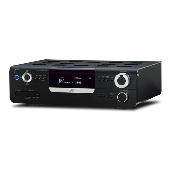
NAD VISO FIVE Service Manual
Dvd surround sound receiver
Hide thumbs
Also See for VISO FIVE:
- Owner's manual (38 pages) ,
- Datasheet (4 pages) ,
- Catalog (20 pages)
Table of Contents
Advertisement
Available languages
Available languages
Advertisement
Chapters
Table of Contents

Related Manuals for NAD VISO FIVE


Summary of Contents for NAD VISO FIVE
- Page 1 Before SN A99VISOFIVE04701...
-
Page 2: Table Of Contents
SECTION 1 SUMMARY CONTENTS PRODUCT SAFETY SERVICING GUIDELINES..................1-4 SERVICING PRECAUTIONS ........................1-5 * General Servicing Precautions * Insulation checking prodedure * Electrostatically Sensitive Devices SPECIFICATIONS ............................1-6 DISASSEMBLY .............................. 1-7 PRINCIPAL PART LOCATION ........................1-8 EXPLODED VIEW ............................1-9... -
Page 3: Product Safety Servicing Guidelines
PRODUCT SAFETY SERVICING GUIDELINES CAUTION : DO NOT ATTEMPT TO MODIFY THIS PRODUCT IN VOLTAGE MEASURE MUST NOT EXCEED 75 VOLTS R.M.S. ANY WAY. NEVER PERFORM CUSTOMIZED INSTALLATIONS THIS CORRESPONDS TO 0.5 MILLIAMP AC ANY VALUE WITHOUT MANUFACTURER’S APPROVAL. UNAUTHORIZED EXCEEDING THIS LIMIT CONSTITUTES A POTENTIAL MODIFICATIONS WILL NOT ONLY VOID THE WARRANTY, BUT SHOCK HAZARD AND MUST BE CORRECTED IMMEDIATELY. -
Page 4: Servicing Precautions
SERVICING PRECAUTIONS CAUTION : Before servicing the A/V Receiver covered by this Electrostatically Sensitive (ES) Devices service data and its supplements and addends, read and follow the Some semiconductor (solid state) devices can be damaged easily by SAFETY PRECAUTIONS. NOTE : if unforeseen circumstances static electricity. -
Page 5: Specifications
SPECIFICATIONS Amplifier Section FM Tuner Section (Without notes 100.1 MHz, 65 dBf) Output Power (Front) : F.T.C Rating: Tuning Range : 60 watts RMS per channel minimum, both channels 87.5 MHz - 108.0 MHz C: 50 kHz steps driven into 8 ohms from 20 Hz to 20kHz with no AH: 100 kHz steps more than 0.09% total harmonic distortion AM Suppression Ratio: C: 50 dB... -
Page 9: Exploded View
EXPLODED VIEW (AH VERSION) CMYL77 1-10... - Page 10 New Part Numbers Non-1W Versions COP11955B-A VISO FIVE FRONT AUTO PCB assembly NON-1W version COP11957B VISO FIVE MAIN AUDIO & MICOM PCB AUTO assembly NON-1W version AH COP11957C-A VISO FIVE MAIN AUDIO & MICOM PCB AUTO assembly NON-1W version C...
- Page 11 EXPLODED VIEW (C VERSION) CMYL77 1-12 1-13...
- Page 12 PCB AUTO assembly NON-1W version AH COP11957C-A VISO FIVE MAIN AUDIO & MICOM PCB AUTO assembly NON-1W version C COP11959B-A VISO FIVE POWER PCB AUTO assembly NON-1W version AH COP11959C-A VISO FIVE POWER PCB AUTO NON-1W version C CIP11958ESMD 1-14...
- Page 13 IC BLOCK DIAGRAMS & PIN DESCRIPTION ..................2-2 TROUBLESHOOTING ..........................2-43 DIAGRAM..............................2-45 1. BLOCK DIAGRAM ..........................2-45 2. WIRING DIAGRAM ..........................2-47 3. SCHEMATIC DIAGRAM ........................2-49 • FRONT PART ..........................2-49 • POWER PART..........................2-51 • MPEG PART..........................2-53 •...
- Page 14 IC BLOCK DIAGRAMS & PIN DESCRIPTION MCU(T5CC1) : IC81 Pin Assignment and Pin Functions The assignment of input/output pins for the T5CC1, their names and functions are as follows: 88 P65 DVCC 87 P64/SCOUT 86 P63/INT0 DVSS 85 P62/SI/SCL P50/AN0 84 P61/SO/SDA P51/AN1 83 P60/SCK...
-
Page 15: Dvcc
DVCC [3] CPU (TLCS-900/L1) DVSS [3] ADTRG (P53) AN0 to AN7 10-Bit 8CH H-OSC (P50 to P57) Clock Gear EMU0 Converter AVCC, AVSS Clock doubler EMU1 VREFH, VREFL XT1 (P96) L-OSC XT2 (P97) TXD0 (P90) RESET SIO/UART/IrDA RXD0 (P91) 32 bits (SIO0) SCLK0/ (P92) - Page 18 I.C PIN DESCRIPTIONS (IC45 : AUDIO DSP : CS494003) Function PIN No PIN Name UHS0 DSP C Control Mode Select BIT 0 DSP C Control Mode Select BIT 0 HUS1 Open-drain interrupt-request output INTREQ,ABODY Host Address Bit One or SPI Serial Control data input FA1,FSCDIN General Purpose output GPIO20...
- Page 19 Function PIN No PIN Name SDRAM Data Bus 14 SD_DATA14 No Connect (Ground) SD_DATA13 SDRAM Data Bus 13 VSSSD3 SDRAM Ground VDDSD3 SDRAM Power Supply SD_DATA12 SDRAM Data Bus 12 SD_DATA11 SDRAM Data Bus 11 SDRAM Data Bus 10 SD_DATA10 SDRAM Data Bus 9 SD_DATA9 SDRAM Data Bus 8...
- Page 20 Function PIN No PIN Name HDATA6 DSP C Bidirectional data bus 6 HDATA5 DSP C Bidirectional data bus 5 SCLK1 Audio output bit clock Audio Master clock MCLK 2.5V Supply Voltage VDD2 VSS2 2.5V Ground AUDATA4 Digital Audio Output 4 HDATA4 DSP C Bidirectional data bus 4 Audio output bit clock...
-
Page 21: Diagram
PIN ASSIGNMENT(IC45: CS494003) AUDATA1 SD_ADDR10, EXTA10 AUDATA0 SD_BA, EXTA19 CMPCLK, FSCLKN2 VDDSD1 HDATA2, GPIO2 VSSSD1 VSS3 SD_CS VDD3 SD_ADDR4, EXTA4 HDATA1, GPIO1 SD_ADDR5, EXTA5 HDATA0, GPIO0 SD_ADDR6, EXTA6 CMPREQ, FLRCLKN2 SD_CLK_EN CMPDAT, FSDATAN2 SD_ADDR7, EXTA7 FLRCLKN1 SD_ADDR8, EXTA8 WR, DS, GPIO10 SD_CLK_IN RD, R/W, GPIO11 SD_ADDR9, EXTA9... - Page 22 CODEC+DIR (AK4589) : IC44 2-10...
- Page 23 PIN DESCRIPTION 2-11...
- Page 24 PIN DESCRIPTION 2-12...
- Page 25 PIN DESCRIPTION 2-13...
- Page 26 VOLUME&FUNCTION (BD3816K1) : IC11 2-14...
- Page 27 2-15...
- Page 28 VIDEO DRIVER IC : IC55 z z z z %ORFN GLDJUDP CTRAP COUT 75Ω MUTE1 MUTE1 TEST TEST 1.5-6M 75Ω MIXOUT MIXFB YTRAP CLAMP CLAMP 75Ω YOUT PYIN PYTRAP PYOUT 75Ω PYFB PbIN PbOUT PrIN 75Ω N.C. MUTE2 MUTE2 PrOUT PrTRAP 75Ω...
- Page 29 XM : IC70 Functional Description I2S_OCLK (M=o, S=n/u) XMDTIC Inter-IC I2S_LRCLK (M=o; S=i) Sound I2S_SCLK (M=o; S=i) (I2S) I2S_DATA (M=o; S=i) I2S_RATE (M=o, S=n/u) MUTE (M=o, S=n/u) 3.3V High Speed HSDP_EN# (M=o; S=i) Data Port HSDP_CLK (M=o; S=i) (HSDP) HSDP_DATA (M=o; S=i) COMM_TX_P COMM_TX_M Low Speed...
- Page 30 Device Pin-out LSDP HSDP_EN# DT4_MODE SC_TX_OUT HSDP_CLK SC_RX_IN HSDP_DATA RFU (I2C_SCL) XM/DT IC RFU (I2C_SDA) TEST Rev 3B/4A SC_RATE ANT_REV OSC_IN RESET# OSC_OUT SLAVE_SEL 2-18...
- Page 31 Pin Descriptions Table 3.2 Pin Descriptions Direct- Function Function Pin Name Notes in Slave Mode in Master Mode S=In Out= 4mA, SLC 1 LSDP Low Speed Data Port Input Low Speed Data Port Output M=Out In=LVTTL S/T S=Out System Controller Bus (CBM) System Controller Bus (CBM) 3 SC_TX_OUT 4mA, SLC...
- Page 32 Direct- Function Function Pin Name Notes in Slave Mode in Master Mode S=In High Speed Data Port Data High Speed Data Port Data Out= 4mA, SLC 32 HSDP_DATA M=Out Input Output In=LVTTL S/T S=In High Speed Data Port Clock High Speed Data Port Clock Out= 4mA, SLC 34 HSDP_CLK M=Out...
- Page 33 SD RAM : IC47 PIN CONFIGURATION DQ15 DQ15 DQ14 DQ14 VSSQ VSSQ DQ13 DQ13 DQ12 DQ12 VDDQ VDDQ DQ11 DQ11 DQ10 DQ10 VSSQ VSSQ VDDQ VDDQ 50pin TSOP II 50pin TSOP II VDDQ VDDQ 400mil x 825mil 400mil x 825mil LDQM LDQM 0.8mm pin pitch...
- Page 34 FUNCTIONAL BLOCK DIAGRAM 1Mx16 Synchronous DRAM Self Refresh Counter Refresh Refresh Interval Timer Counter 512Kx16 Bank 0 Address[0:10] Sense AMP & I/O gates Column Decoder Address Precharge Register Row Active BA(A11) Column Addr. Column Active Latch & Counter Overflow Burst Length Counter DQ10 DQ11...
-
Page 35: Dvss
64M SDRAM (M12L64164A) : IC12 PIN ASSIGNMENT FUNCTIONAL BLOCK DIAGRAM Top View DQ15 DQ 0 D D Q S S Q DQ14 Clock DQ 1 Generator Bank D DQ 2 DQ13 Bank C D D Q S S Q Bank B DQ12 DQ 3 Address... - Page 36 Motor Driver IC (AM5888) : IC16 2-24...
- Page 37 2-25...
- Page 38 Pin description PIN No Pin Name Function VINFC Input for focus driver TRB_1 Connect to external transistor base REGO2 Regulator voltage output, connect to external transistor collector VINSL+ Input for the sled driver REGO1 Regulator voltage output, connect to external transistor collector Tray driver forward input Tray driver reverse input Vcc1...
- Page 39 Flash Memory (M29W160ET) : IC11 Signal Names Logic Diagram A0-A19 Address Inputs DQ0-DQ7 Data Inputs/Outputs V CC DQ8-DQ14 Data Inputs/Outputs DQ15A–1 Data Input/Output or Address Input A0-A19 DQ0-DQ14 Chip Enable DQ15A–1 Output Enable M29W160ET Write Enable M29W160EB Reset/Block Temporary Unprotect Ready/Busy Output BYTE BYTE...
- Page 40 UART IC : IC70 XR20M1170 B LOCK IAGRAM 1.62V – 3.63V 64 Byte TX FIFO ENIR# 64 Byte EN485# UART RX FIFO IRQ# Regs RTS# CTS# GPIOs C/SPI GPIO[7:0] A0/CS# Interface A1/SI XTAL1 Crystal Osc/Buffer XTAL2 I2C/SPI# 2-28...
- Page 41 VIDEO SW IC (NJM2595) : IC51, IC52, IC53 5-INPUT 3-OUTPUT VIDEO SWITCH • • 5-input 3-output • Operating Voltage 4.0 to 6.5V • Operating current 15mAtyp. at Vcc= 5V • Crosstalk -65dBtyp. • Internal 6dB Amplifier • Internal 75 Driver •...
- Page 42 INVERTER IC (TC74HCU04AFN) : IC36 PIN ASSIGNMENT LOGIC SYMBOL (10) (11) (13) (12) TRUTH TABLE 2-30...
- Page 43 LOGIC IC : IC88(74LCX08MX) Logic Symbol Connection Diagrams IEEE/IEC Pin Assignments for SOIC, SOP, and TSSOP Pad Assignments for DQFN Pin Descriptions Pin Names Description Inputs Outputs (Top View) OPA 2134UA / N JM 2068MD (OP A M P) • P IN F UNC IT ON 1.
- Page 44 OR GATE : IC48(74LCX32TTR) Pin Connection And IEC Logic Symbols AND GATE : IC80(74LVC08ADR) PIN CONFIGURATION LOGIC SYMBOL SV00435 SY00034 PIN DESCRIPTION PIN NUMBER SYMBOL NAME AND FUNCTION 1, 4, 9, 12 1A – 4A Data inputs Data inputs 2, 5, 10, 13 1B –...
- Page 45 MULTIPLEXERS : IC35(74LVC157ADBR) Inputs can be driven from either 3.3-V or 5-V devices. This feature allows the use of these devices as translators in a mixed 3.3-V/5-V system environment. FUNCTION TABLE INPUTS OUTPUT OUTPUT logic diagram (positive logic) Pin numbers shown are for the D, DB, J, NS, PW, RGY, and W packages. 2-33...
-
Page 46: Dvss
2CH DAC : IC71(AK4384) LRCK MCLK Clock De-emphasis SMUTE/CSN μP Divider Control VCOM ACKS/CCLK Interface DIF0/CDTI DZFL DZFR ΔΣ AOUTL Modulator Interpolator Audio Data BICK Interface ΔΣ SDTI AOUTR Interpolator Modulator 2-34... - Page 47 Pin Layout MCLK DZFL BICK DZFR SDTI LRCK View VCOM SMUTE/CSN AOUTL ACKS/CCLK AOUTR DIF0/CDTI PIN/FUNCTION Pin Name Function MCLK Master Clock Input Pin An external TTL clock should be input on this pin. BICK Audio Serial Data Clock Pin SDTI Audio Serial Data Input Pin LRCK...
- Page 48 EEPROM : IC13(AT24C08N10SC) 2-36...
- Page 49 FET : IC14(HN1K05FU) Equivalent Circuit Marking (top view) (Q1, Q2 common) Switching Time Test Circuit (a) Test circuit (b) V 1.5 V = 1.5 V 1.5 V D.U. < = 1% < 5 ns = 50 W) (c) V Common Source 10 ms Ta = 25°C DS (ON)
- Page 50 RDS DEMODULATION IC(LC72723M) : IC89 Pin Assignment Block Diagram 2-38...
- Page 51 VIDEO SW IC(PI5V330) : IC56, IC59 Low On-Resistance Wideband/Video Quad 2-Channel Mux/DeMux Features Description • High-performance solution to switch between video sources Pericom Semiconductor’s PI5V330 is a true bidirectional Quad 2-channel multiplexer/demultiplexer recommended for both RGB • Wide bandwidth: 200 MHz and composite video switching applications.
-
Page 52: Reset
RESET IC(RH5VT18C) : IC85 BLOCK DIAGRAMS – Vref TIME CHART Released Voltage Detector Threshold Hysteresis Detected Voltage –V Supply Voltage Minimum Operating Voltage Output Voltage (OUT) DEFINITION OF OUTPUT DELAY TIME t + 2.0V Input Voltage 0.7V +2.0V Output Voltage + 2.0V 2-40... - Page 53 RS232 TRANSCEIVER : IC21 PIN CONFIGURATION PIN DESCRIPTION PIN No SYMBOL NAME AND F UNCTION Positive Terminal for the first Charge Pump Capacitor Doubled Voltage Terminal Negative Terminal for the first Charge Pump Capacitor Positive Terminal for the second Charge Pump Capacitor Negative Terminal for the second Charge Pump Capacitor Inverted Voltage Terminal Second Transmitter Output Voltage...
- Page 54 TRANSISTOR, REGULATOR IC BLOCK DIAGRAM TO-92S TO-92 TO-220 TO-92L 1. Emitter 1. Emitter 1. Emitter 1. INPUT 2. Collector 2. Collector 2. Collector 2. OUTPUT 3. Base 3. Base 3. Base 3. GND 1 23 1 23 1 2 3 1 2 3 KRA102M KRC102M...
- Page 55 2-43...
- Page 56 2-44...
- Page 57 1. BLOCK DIAGRAM 2-45 2-46...
- Page 58 2. WIRING DIAGRAM 2-47 2-48...
-
Page 59: Schematic Diagram
3. SCHEMATIC DIAGRAM FRONT PART 2-49 2-50... -
Page 60: Power Part
POWER PART 2-51a 2-51b... -
Page 64: Mpeg Part
MPEG PART 2-53 2-54... -
Page 65: Video & Xm & Dab Part
VIDEO&XM&DAB PART 2-55 2-56... - Page 66 VIDEO&XM&DAB PART 2-57 2-58...
-
Page 67: Amp Part
AMP PART 2-59 2-60... -
Page 68: Printed Circuit Boards
4. PRINTED CIRCUIT BOARDS FRONT PCB DATA VIEW 2-61 2-62... - Page 69 POWER PCB DATA VIEW 2-63 2-64...
- Page 70 MPEG & HDMI PCB DATA VIEW TOP VIEW BOTTOM VIEW 2-65 2-66...
- Page 71 MAIN AUDIO & MICOM PCB DATA VIEW TOP VIEW 2-67 2-68...
- Page 72 MAIN AUDIO & MICOM PCB DATA VIEW BOTTOM VIEW 2-69 2-70...
- Page 73 VIDEO XM (AH) DAB (C) PCB DATA VIEW TOP VIEW 2-71 2-72...
- Page 74 VIDEO EX (AH) XM (C) PCB DATA VIEW BOTTOM VIEW 2-73 2-74...
- Page 75 AMP PCB DATA VIEW 2-75 2-76...
- Page 76 SECTION 3 ELECTRICAL PARTS LIST RESISTORS AND CAPACITORS Notes : * Please use this part number for parts order. * IMPORTANT SAFETY NOTICE. Components identified by mark have special characteristics important for safety. When replacing any of these components, use only manufacture's specified parts. * The unit of resistance is ohm( ) k=1000 , M=1000...
- Page 86 3-11...
- Page 87 3-12...
- Page 88 3-13...
- Page 89 3-14...
- Page 90 3-15...
- Page 91 3-16...
- Page 92 3-17...
- Page 93 3-18...
- Page 94 3-19...
- Page 96 3-21...
- Page 97 3-22...
- Page 98 3-23...
- Page 99 3-24...
- Page 100 3-25...
- Page 101 3-26...
- Page 102 3-27...
- Page 103 3-28...
- Page 104 3-29...
- Page 106 3-31...
- Page 107 3-32...
- Page 108 3-33...
- Page 109 Assembly with heatsink & fan is CMYL77 3-34...
- Page 110 3-35...
- Page 111 3-36...
- Page 112 3-37...
- Page 113 3-38...
- Page 114 3-39...
- Page 116 3-41...
- Page 117 3-42...
- Page 118 3-43...
- Page 119 3-44...
- Page 120 3-45...
- Page 121 3-46...
- Page 122 3-47...
- Page 123 3-48...